JP2007011069A - 液晶表示素子及びその製造方法 - Google Patents
液晶表示素子及びその製造方法 Download PDFInfo
- Publication number
- JP2007011069A JP2007011069A JP2005192805A JP2005192805A JP2007011069A JP 2007011069 A JP2007011069 A JP 2007011069A JP 2005192805 A JP2005192805 A JP 2005192805A JP 2005192805 A JP2005192805 A JP 2005192805A JP 2007011069 A JP2007011069 A JP 2007011069A
- Authority
- JP
- Japan
- Prior art keywords
- liquid crystal
- alignment
- crystal display
- display element
- film
- Prior art date
- Legal status (The legal status is an assumption and is not a legal conclusion. Google has not performed a legal analysis and makes no representation as to the accuracy of the status listed.)
- Granted
Links
Images


Classifications
-
- G—PHYSICS
- G02—OPTICS
- G02F—OPTICAL DEVICES OR ARRANGEMENTS FOR THE CONTROL OF LIGHT BY MODIFICATION OF THE OPTICAL PROPERTIES OF THE MEDIA OF THE ELEMENTS INVOLVED THEREIN; NON-LINEAR OPTICS; FREQUENCY-CHANGING OF LIGHT; OPTICAL LOGIC ELEMENTS; OPTICAL ANALOGUE/DIGITAL CONVERTERS
- G02F1/00—Devices or arrangements for the control of the intensity, colour, phase, polarisation or direction of light arriving from an independent light source, e.g. switching, gating or modulating; Non-linear optics
- G02F1/01—Devices or arrangements for the control of the intensity, colour, phase, polarisation or direction of light arriving from an independent light source, e.g. switching, gating or modulating; Non-linear optics for the control of the intensity, phase, polarisation or colour
- G02F1/13—Devices or arrangements for the control of the intensity, colour, phase, polarisation or direction of light arriving from an independent light source, e.g. switching, gating or modulating; Non-linear optics for the control of the intensity, phase, polarisation or colour based on liquid crystals, e.g. single liquid crystal display cells
- G02F1/133—Constructional arrangements; Operation of liquid crystal cells; Circuit arrangements
- G02F1/1333—Constructional arrangements; Manufacturing methods
- G02F1/1339—Gaskets; Spacers; Sealing of cells
- G02F1/13394—Gaskets; Spacers; Sealing of cells spacers regularly patterned on the cell subtrate, e.g. walls, pillars
-
- G—PHYSICS
- G02—OPTICS
- G02F—OPTICAL DEVICES OR ARRANGEMENTS FOR THE CONTROL OF LIGHT BY MODIFICATION OF THE OPTICAL PROPERTIES OF THE MEDIA OF THE ELEMENTS INVOLVED THEREIN; NON-LINEAR OPTICS; FREQUENCY-CHANGING OF LIGHT; OPTICAL LOGIC ELEMENTS; OPTICAL ANALOGUE/DIGITAL CONVERTERS
- G02F1/00—Devices or arrangements for the control of the intensity, colour, phase, polarisation or direction of light arriving from an independent light source, e.g. switching, gating or modulating; Non-linear optics
- G02F1/01—Devices or arrangements for the control of the intensity, colour, phase, polarisation or direction of light arriving from an independent light source, e.g. switching, gating or modulating; Non-linear optics for the control of the intensity, phase, polarisation or colour
- G02F1/13—Devices or arrangements for the control of the intensity, colour, phase, polarisation or direction of light arriving from an independent light source, e.g. switching, gating or modulating; Non-linear optics for the control of the intensity, phase, polarisation or colour based on liquid crystals, e.g. single liquid crystal display cells
- G02F1/133—Constructional arrangements; Operation of liquid crystal cells; Circuit arrangements
- G02F1/1333—Constructional arrangements; Manufacturing methods
- G02F1/1337—Surface-induced orientation of the liquid crystal molecules, e.g. by alignment layers
- G02F1/133707—Structures for producing distorted electric fields, e.g. bumps, protrusions, recesses, slits in pixel electrodes
-
- G—PHYSICS
- G02—OPTICS
- G02F—OPTICAL DEVICES OR ARRANGEMENTS FOR THE CONTROL OF LIGHT BY MODIFICATION OF THE OPTICAL PROPERTIES OF THE MEDIA OF THE ELEMENTS INVOLVED THEREIN; NON-LINEAR OPTICS; FREQUENCY-CHANGING OF LIGHT; OPTICAL LOGIC ELEMENTS; OPTICAL ANALOGUE/DIGITAL CONVERTERS
- G02F1/00—Devices or arrangements for the control of the intensity, colour, phase, polarisation or direction of light arriving from an independent light source, e.g. switching, gating or modulating; Non-linear optics
- G02F1/01—Devices or arrangements for the control of the intensity, colour, phase, polarisation or direction of light arriving from an independent light source, e.g. switching, gating or modulating; Non-linear optics for the control of the intensity, phase, polarisation or colour
- G02F1/13—Devices or arrangements for the control of the intensity, colour, phase, polarisation or direction of light arriving from an independent light source, e.g. switching, gating or modulating; Non-linear optics for the control of the intensity, phase, polarisation or colour based on liquid crystals, e.g. single liquid crystal display cells
- G02F1/133—Constructional arrangements; Operation of liquid crystal cells; Circuit arrangements
- G02F1/1333—Constructional arrangements; Manufacturing methods
- G02F1/1337—Surface-induced orientation of the liquid crystal molecules, e.g. by alignment layers
- G02F1/13378—Surface-induced orientation of the liquid crystal molecules, e.g. by alignment layers by treatment of the surface, e.g. embossing, rubbing or light irradiation
- G02F1/133784—Surface-induced orientation of the liquid crystal molecules, e.g. by alignment layers by treatment of the surface, e.g. embossing, rubbing or light irradiation by rubbing
-
- G—PHYSICS
- G02—OPTICS
- G02F—OPTICAL DEVICES OR ARRANGEMENTS FOR THE CONTROL OF LIGHT BY MODIFICATION OF THE OPTICAL PROPERTIES OF THE MEDIA OF THE ELEMENTS INVOLVED THEREIN; NON-LINEAR OPTICS; FREQUENCY-CHANGING OF LIGHT; OPTICAL LOGIC ELEMENTS; OPTICAL ANALOGUE/DIGITAL CONVERTERS
- G02F1/00—Devices or arrangements for the control of the intensity, colour, phase, polarisation or direction of light arriving from an independent light source, e.g. switching, gating or modulating; Non-linear optics
- G02F1/01—Devices or arrangements for the control of the intensity, colour, phase, polarisation or direction of light arriving from an independent light source, e.g. switching, gating or modulating; Non-linear optics for the control of the intensity, phase, polarisation or colour
- G02F1/13—Devices or arrangements for the control of the intensity, colour, phase, polarisation or direction of light arriving from an independent light source, e.g. switching, gating or modulating; Non-linear optics for the control of the intensity, phase, polarisation or colour based on liquid crystals, e.g. single liquid crystal display cells
- G02F1/133—Constructional arrangements; Operation of liquid crystal cells; Circuit arrangements
- G02F1/1333—Constructional arrangements; Manufacturing methods
- G02F1/1337—Surface-induced orientation of the liquid crystal molecules, e.g. by alignment layers
- G02F1/13378—Surface-induced orientation of the liquid crystal molecules, e.g. by alignment layers by treatment of the surface, e.g. embossing, rubbing or light irradiation
- G02F1/133788—Surface-induced orientation of the liquid crystal molecules, e.g. by alignment layers by treatment of the surface, e.g. embossing, rubbing or light irradiation by light irradiation, e.g. linearly polarised light photo-polymerisation
Landscapes
- Physics & Mathematics (AREA)
- Nonlinear Science (AREA)
- Mathematical Physics (AREA)
- Chemical & Material Sciences (AREA)
- Crystallography & Structural Chemistry (AREA)
- General Physics & Mathematics (AREA)
- Optics & Photonics (AREA)
- Spectroscopy & Molecular Physics (AREA)
- Liquid Crystal (AREA)
Abstract
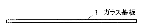
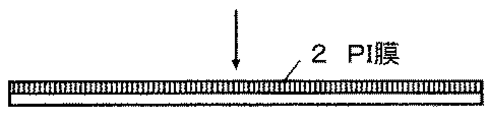
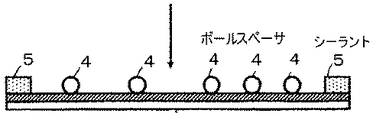
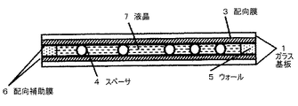
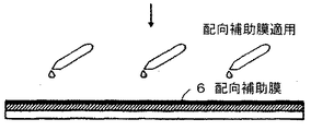
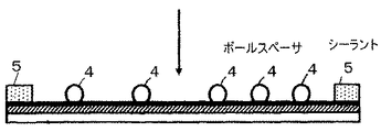
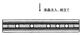
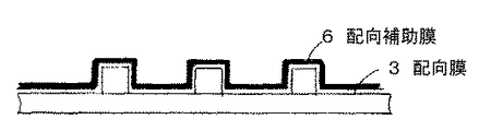
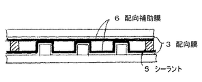
【解決課題】 配向処理された配向膜を上に、結晶性エポキシ樹脂を予め有機溶媒に溶解させた結晶性エポキシ樹脂溶液を配向処理後の配向膜上に塗布し、配向補助膜6を形成する。次に、従来技術と同様に、スペーサボール4を散布し、基板周辺に接着剤を塗布してウォール5を形成する(図3F)。次いで、図3Gに示すように、配向処理された配向膜上に配向補助膜6が形成されたもう一方のガラス基板と重ね合わせ、液晶を注入し偏光板を形成して液晶パネルセルを製造する。
【選択図】 図2
Description
前記一対の基板が、配向膜及び前記配向膜上に形成された配向補助膜を有し、それら基板が互いに前記配向補助膜が対向するように液晶を介して配置され、
前記配向補助膜は、分子骨格にメソゲン構造を有し両端に熱又は紫外線で反応する反応基を有する樹脂材料よりなる、
ことを特徴とする液晶表示素子を提供する。
(I)前記一対の基板の一方の基板上に配向膜を形成する工程、
(II)前記配向膜上に、分子骨格にメソゲン構造を有し両端に熱又は紫外線で反応する反応基を有する樹脂材料を有機溶剤で希釈した溶液を塗布する工程、
(III)前記塗布された溶液から前記有機溶剤を蒸発させて配向補助膜を形成する工程、及び
(IV)上記と同様の工程により配向膜及びその上に配向補助膜が形成された他方の基板を、前記配向補助膜が対向するように重ね合わせ両者を接着する工程
を含むことを特徴とする液晶表示素子の製造方法を提供する。
なお、本発明は下記実施例に限定されるものではなく、本特許請求の範囲に規定された範囲において種々の修正及び変更を加えることができることは明らかである。
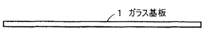
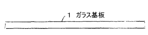
2 PI膜
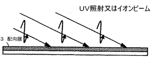
3 配向膜
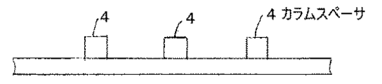
4 スペーサボール
5 ウォール
6 配向補助膜
7 液晶
Claims (17)
- 一対の基板に液晶を狭持してなる液晶表示素子であって、
前記一対の基板が、配向膜及び前記配向膜上に形成された配向補助膜を有し、それら基板が互いに前記配向補助膜が対向するように液晶を介して配置され、
前記配向補助膜は、分子骨格にメソゲン構造を有し両端に熱又は紫外線で反応する反応基を有する樹脂材料よりなる、
ことを特徴とする液晶表示素子 - 前記対向する一対の基板間に、ボールスペーサが介在することを特徴とする請求項1記載の液晶表示素子。
- 前記対向する一対の基板のうちの一方の基板上の配向膜及び配向補助膜が、カラムスペーサを介して形成されていることを特徴とする請求項1記載の液晶表示素子。
- 前記樹脂材料が、結晶性エポキシ樹脂であることを特徴とする請求項1記載の液晶表示素子。
- 前記結晶性エポキシ樹脂が、ビフェニル型エポキシであることを特徴とする請求項4記載の液晶表示素子。
- 前記樹脂材料の分子が、両端にグリシジルエーテルを有することを特徴とする請求項1記載の液晶表示素子。
- 前記配向補助膜が、100Åを超える膜厚であって、4000Å以下の膜厚を有することを特徴とする請求項1記載の液晶表示素子。
- 前記配向補助膜が、300Å以上、1000Å以下の膜厚を有することを特徴とする請求項7記載の液晶表示素子。
- 一対の基板に液晶を狭持してなる液晶表示素子の製造方法であって、
(I)前記一対の基板の一方の基板上に配向膜を形成する工程、
(II)前記配向膜上に、分子骨格にメソゲン構造を有し両端に熱又は紫外線で反応する反応基を有する樹脂材料を有機溶剤で希釈した溶液を塗布する工程、
(III)前記塗布された溶液から前記有機溶剤を蒸発させて配向補助膜を形成する工程、及び
(IV)上記と同様の工程により配向膜及びその上に配向補助膜が形成された他方の基板を、双方の前記配向補助膜が対向するように重ね合わせ両者を接着する工程
を含むことを特徴とする液晶表示素子の製造方法。 - 請求項9の工程(III)の後、ボールスペーサが配向補助膜上に散布されることを特徴とする請求項9記載の液晶表示素子の製造方法。
- 請求項9の工程(I)おいて、前記一方の基板上に配向膜がカラムスペーサを介して形成されることを特徴とする請求項9記載の液晶表示素子の製造方法。
- 前記樹脂材料が、結晶性エポキシ樹脂であることを特徴とする請求項9記載の液晶表示素子。
- 前記結晶性エポキシ樹脂が、ビフェニル型エポキシであることを特徴とする請求項12記載の液晶表示素子の製造方法。
- 前記溶液中の前記樹脂材料が、0.001%を超える濃度であって、1.0%未満の濃度で含有されることを特徴とする請求項9記載の液晶表示素子の製造方法。
- 前記溶液中の前記樹脂材料が、0.01%以上0.1%以下の濃度で含有されることを特徴とする請求項14記載の液晶表示素子の製造方法。
- 前記有機溶剤を蒸発させる工程は、加熱又は減圧により行うことを特徴とする請求項9記載の液晶表示素子の製造方法。
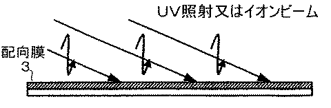
- 請求項1の工程(I)の後に、前記配向膜を、ラビング、UV照射及びイオンビームの中の1つを利用して配向を行うことを特徴とする請求項9記載の液晶表示素子の製造方法。
Priority Applications (2)
| Application Number | Priority Date | Filing Date | Title |
|---|---|---|---|
| JP2005192805A JP4546340B2 (ja) | 2005-06-30 | 2005-06-30 | 液晶表示素子の製造方法 |
| KR1020050080227A KR101030533B1 (ko) | 2005-06-30 | 2005-08-30 | 액정표시소자의 제조방법 |
Applications Claiming Priority (1)
| Application Number | Priority Date | Filing Date | Title |
|---|---|---|---|
| JP2005192805A JP4546340B2 (ja) | 2005-06-30 | 2005-06-30 | 液晶表示素子の製造方法 |
Publications (2)
| Publication Number | Publication Date |
|---|---|
| JP2007011069A true JP2007011069A (ja) | 2007-01-18 |
| JP4546340B2 JP4546340B2 (ja) | 2010-09-15 |
Family
ID=37749659
Family Applications (1)
| Application Number | Title | Priority Date | Filing Date |
|---|---|---|---|
| JP2005192805A Expired - Fee Related JP4546340B2 (ja) | 2005-06-30 | 2005-06-30 | 液晶表示素子の製造方法 |
Country Status (2)
| Country | Link |
|---|---|
| JP (1) | JP4546340B2 (ja) |
| KR (1) | KR101030533B1 (ja) |
Cited By (6)
| Publication number | Priority date | Publication date | Assignee | Title |
|---|---|---|---|---|
| JP2009086265A (ja) * | 2007-09-28 | 2009-04-23 | Lg Display Co Ltd | 配向膜の製造方法および液晶パネルの製造方法 |
| WO2012090838A1 (ja) * | 2010-12-28 | 2012-07-05 | シャープ株式会社 | 液晶パネル、及び、液晶ディスプレイ |
| CN103588957A (zh) * | 2012-08-16 | 2014-02-19 | Lg伊诺特有限公司 | 环氧树脂组合物以及使用该环氧树脂组合物的辐射热电路板 |
| JP2015152808A (ja) * | 2014-02-17 | 2015-08-24 | Dic株式会社 | 液晶配向補助剤およびこれを用いた液晶表示素子 |
| CN109445199A (zh) * | 2018-12-30 | 2019-03-08 | 厦门天马微电子有限公司 | 一种液晶装置及其制备方法 |
| CN113419382A (zh) * | 2021-06-30 | 2021-09-21 | 深圳市华星光电半导体显示技术有限公司 | 显示面板的制作方法 |
Families Citing this family (2)
| Publication number | Priority date | Publication date | Assignee | Title |
|---|---|---|---|---|
| KR20100130762A (ko) | 2009-06-04 | 2010-12-14 | 삼성전자주식회사 | 편광막을 포함하는 표시 장치와 그의 제조방법 |
| KR102717155B1 (ko) * | 2021-12-28 | 2024-10-14 | 동우 화인켐 주식회사 | 광학 적층체 및 이의 제조방법과, 이를 포함하는 스마트 윈도우 및 이를 적용한 자동차 또는 건물용 창호 |
Citations (5)
| Publication number | Priority date | Publication date | Assignee | Title |
|---|---|---|---|---|
| JPH10268318A (ja) * | 1997-03-06 | 1998-10-09 | Sharp Corp | 光学装置および液晶表示装置ならびに光学装置の製造方法 |
| JPH10330756A (ja) * | 1997-06-05 | 1998-12-15 | Sumitomo Bakelite Co Ltd | 液晶配向剤及びそれを用いた液晶表示素子 |
| WO2002003131A1 (fr) * | 2000-07-04 | 2002-01-10 | Nec Corporation | Procede et dispositif d'affichage a cristaux liquides, et appareil de fabrication d'affichage a cristaux liquides |
| JP2005258428A (ja) * | 2004-02-10 | 2005-09-22 | Dainippon Printing Co Ltd | 液晶表示素子 |
| WO2006123791A1 (ja) * | 2005-05-19 | 2006-11-23 | Dai Nippon Printing Co., Ltd. | 液晶表示素子および液晶表示素子の製造方法 |
Family Cites Families (1)
| Publication number | Priority date | Publication date | Assignee | Title |
|---|---|---|---|---|
| JP4393662B2 (ja) * | 2000-03-17 | 2010-01-06 | 株式会社半導体エネルギー研究所 | 液晶表示装置の作製方法 |
-
2005
- 2005-06-30 JP JP2005192805A patent/JP4546340B2/ja not_active Expired - Fee Related
- 2005-08-30 KR KR1020050080227A patent/KR101030533B1/ko not_active Expired - Lifetime
Patent Citations (5)
| Publication number | Priority date | Publication date | Assignee | Title |
|---|---|---|---|---|
| JPH10268318A (ja) * | 1997-03-06 | 1998-10-09 | Sharp Corp | 光学装置および液晶表示装置ならびに光学装置の製造方法 |
| JPH10330756A (ja) * | 1997-06-05 | 1998-12-15 | Sumitomo Bakelite Co Ltd | 液晶配向剤及びそれを用いた液晶表示素子 |
| WO2002003131A1 (fr) * | 2000-07-04 | 2002-01-10 | Nec Corporation | Procede et dispositif d'affichage a cristaux liquides, et appareil de fabrication d'affichage a cristaux liquides |
| JP2005258428A (ja) * | 2004-02-10 | 2005-09-22 | Dainippon Printing Co Ltd | 液晶表示素子 |
| WO2006123791A1 (ja) * | 2005-05-19 | 2006-11-23 | Dai Nippon Printing Co., Ltd. | 液晶表示素子および液晶表示素子の製造方法 |
Cited By (7)
| Publication number | Priority date | Publication date | Assignee | Title |
|---|---|---|---|---|
| JP2009086265A (ja) * | 2007-09-28 | 2009-04-23 | Lg Display Co Ltd | 配向膜の製造方法および液晶パネルの製造方法 |
| WO2012090838A1 (ja) * | 2010-12-28 | 2012-07-05 | シャープ株式会社 | 液晶パネル、及び、液晶ディスプレイ |
| CN103588957A (zh) * | 2012-08-16 | 2014-02-19 | Lg伊诺特有限公司 | 环氧树脂组合物以及使用该环氧树脂组合物的辐射热电路板 |
| JP2015152808A (ja) * | 2014-02-17 | 2015-08-24 | Dic株式会社 | 液晶配向補助剤およびこれを用いた液晶表示素子 |
| CN109445199A (zh) * | 2018-12-30 | 2019-03-08 | 厦门天马微电子有限公司 | 一种液晶装置及其制备方法 |
| CN109445199B (zh) * | 2018-12-30 | 2021-11-23 | 厦门天马微电子有限公司 | 一种液晶装置及其制备方法 |
| CN113419382A (zh) * | 2021-06-30 | 2021-09-21 | 深圳市华星光电半导体显示技术有限公司 | 显示面板的制作方法 |
Also Published As
| Publication number | Publication date |
|---|---|
| KR101030533B1 (ko) | 2011-04-21 |
| KR20070003500A (ko) | 2007-01-05 |
| JP4546340B2 (ja) | 2010-09-15 |
Similar Documents
| Publication | Publication Date | Title |
|---|---|---|
| US8724073B2 (en) | Method for manufacturing liquid crystal display device comprising applying adhesive solution on column spacers and sidewall | |
| TWI425281B (zh) | 聚合物穩定配向型液晶顯示面板的製造方法 | |
| US8178288B2 (en) | Method for fabricating display substrate and liquid crystal display | |
| KR20060130386A (ko) | 액정표시소자 및 그 제조방법 | |
| CN1485664A (zh) | 显示板及其用于该显示板制备的多层极板 | |
| JP4546340B2 (ja) | 液晶表示素子の製造方法 | |
| WO2015146369A1 (ja) | 液晶表示装置、及び、液晶表示装置の製造方法 | |
| US8325304B2 (en) | Method of fabricating liquid crystal display | |
| US7782414B2 (en) | Method for fabricating in-plane switching mode liquid crystal display device | |
| US7501163B2 (en) | Liquid crystal display device and method for manufacturing the same | |
| JPH04356020A (ja) | 液晶配向膜及びその製造方法並びに液晶表示装置及びその製造方法 | |
| JP4320338B2 (ja) | 液晶パネルセルの製造方法 | |
| JP2018005040A (ja) | 調光フィルム、調光フィルムの製造方法 | |
| CN105676540B (zh) | 液晶显示面板的制作方法 | |
| Park et al. | Liquid crystal cell process | |
| JPH037913A (ja) | 液晶配向膜とその製造方法およびそれを用いた液晶表示装置 | |
| JP3301960B2 (ja) | 液晶配向膜、液晶配向膜の製造方法、液晶表示装置及び液晶表示装置の製造方法 | |
| KR100631753B1 (ko) | 광학 필름 | |
| CN113867052A (zh) | 显示面板的光配向方法、显示面板和显示装置 | |
| JPH07239475A (ja) | 液晶分子の配向法 | |
| KR101309860B1 (ko) | 필름형 시일 테이프의 제조 방법 및 필름형 시일 테이프를이용한 액정 표시 장치의 제조 방법 | |
| JPS6114623A (ja) | 液晶セル用配向処理剤 | |
| JPH0416925A (ja) | 液晶素子およびその製造方法 | |
| JPH05249471A (ja) | 液晶表示素子 | |
| KR20040095061A (ko) | 액정표시장치의 제조방법 |
Legal Events
| Date | Code | Title | Description |
|---|---|---|---|
| A621 | Written request for application examination |
Free format text: JAPANESE INTERMEDIATE CODE: A621 Effective date: 20080627 |
|
| A131 | Notification of reasons for refusal |
Free format text: JAPANESE INTERMEDIATE CODE: A131 Effective date: 20081203 |
|
| A521 | Request for written amendment filed |
Free format text: JAPANESE INTERMEDIATE CODE: A523 Effective date: 20090303 |
|
| A131 | Notification of reasons for refusal |
Free format text: JAPANESE INTERMEDIATE CODE: A131 Effective date: 20090427 |
|
| A521 | Request for written amendment filed |
Free format text: JAPANESE INTERMEDIATE CODE: A523 Effective date: 20090724 |
|
| A131 | Notification of reasons for refusal |
Free format text: JAPANESE INTERMEDIATE CODE: A131 Effective date: 20090914 |
|
| A601 | Written request for extension of time |
Free format text: JAPANESE INTERMEDIATE CODE: A601 Effective date: 20091214 |
|
| A602 | Written permission of extension of time |
Free format text: JAPANESE INTERMEDIATE CODE: A602 Effective date: 20091217 |
|
| A521 | Request for written amendment filed |
Free format text: JAPANESE INTERMEDIATE CODE: A523 Effective date: 20100315 |
|
| TRDD | Decision of grant or rejection written | ||
| A01 | Written decision to grant a patent or to grant a registration (utility model) |
Free format text: JAPANESE INTERMEDIATE CODE: A01 Effective date: 20100607 |
|
| A01 | Written decision to grant a patent or to grant a registration (utility model) |
Free format text: JAPANESE INTERMEDIATE CODE: A01 |
|
| A61 | First payment of annual fees (during grant procedure) |
Free format text: JAPANESE INTERMEDIATE CODE: A61 Effective date: 20100701 |
|
| FPAY | Renewal fee payment (event date is renewal date of database) |
Free format text: PAYMENT UNTIL: 20130709 Year of fee payment: 3 |
|
| R150 | Certificate of patent or registration of utility model |
Ref document number: 4546340 Country of ref document: JP Free format text: JAPANESE INTERMEDIATE CODE: R150 Free format text: JAPANESE INTERMEDIATE CODE: R150 |
|
| R250 | Receipt of annual fees |
Free format text: JAPANESE INTERMEDIATE CODE: R250 |
|
| R250 | Receipt of annual fees |
Free format text: JAPANESE INTERMEDIATE CODE: R250 |
|
| R250 | Receipt of annual fees |
Free format text: JAPANESE INTERMEDIATE CODE: R250 |
|
| R250 | Receipt of annual fees |
Free format text: JAPANESE INTERMEDIATE CODE: R250 |
|
| R250 | Receipt of annual fees |
Free format text: JAPANESE INTERMEDIATE CODE: R250 |
|
| R250 | Receipt of annual fees |
Free format text: JAPANESE INTERMEDIATE CODE: R250 |
|
| R250 | Receipt of annual fees |
Free format text: JAPANESE INTERMEDIATE CODE: R250 |
|
| R250 | Receipt of annual fees |
Free format text: JAPANESE INTERMEDIATE CODE: R250 |
|
| R250 | Receipt of annual fees |
Free format text: JAPANESE INTERMEDIATE CODE: R250 |
|
| LAPS | Cancellation because of no payment of annual fees |