JP2007142475A - 半導体装置およびその製造方法 - Google Patents
半導体装置およびその製造方法 Download PDFInfo
- Publication number
- JP2007142475A JP2007142475A JP2007046498A JP2007046498A JP2007142475A JP 2007142475 A JP2007142475 A JP 2007142475A JP 2007046498 A JP2007046498 A JP 2007046498A JP 2007046498 A JP2007046498 A JP 2007046498A JP 2007142475 A JP2007142475 A JP 2007142475A
- Authority
- JP
- Japan
- Prior art keywords
- interlayer film
- semiconductor device
- film
- etching
- contact hole
- Prior art date
- Legal status (The legal status is an assumption and is not a legal conclusion. Google has not performed a legal analysis and makes no representation as to the accuracy of the status listed.)
- Pending
Links
- 239000004065 semiconductor Substances 0.000 title claims abstract description 42
- 238000004519 manufacturing process Methods 0.000 title claims abstract description 22
- 239000011229 interlayer Substances 0.000 claims abstract description 84
- 238000005530 etching Methods 0.000 claims abstract description 45
- 239000000758 substrate Substances 0.000 claims description 15
- 150000004767 nitrides Chemical class 0.000 claims description 2
- 238000010030 laminating Methods 0.000 claims 4
- 229910052581 Si3N4 Inorganic materials 0.000 abstract description 10
- HQVNEWCFYHHQES-UHFFFAOYSA-N silicon nitride Chemical compound N12[Si]34N5[Si]62N3[Si]51N64 HQVNEWCFYHHQES-UHFFFAOYSA-N 0.000 abstract description 10
- 238000009792 diffusion process Methods 0.000 abstract description 5
- 239000003112 inhibitor Substances 0.000 abstract 2
- 239000010410 layer Substances 0.000 abstract 1
- 239000010949 copper Substances 0.000 description 12
- 229910052751 metal Inorganic materials 0.000 description 11
- 239000002184 metal Substances 0.000 description 11
- RYGMFSIKBFXOCR-UHFFFAOYSA-N Copper Chemical compound [Cu] RYGMFSIKBFXOCR-UHFFFAOYSA-N 0.000 description 6
- 229910052802 copper Inorganic materials 0.000 description 6
- 238000000034 method Methods 0.000 description 6
- VYPSYNLAJGMNEJ-UHFFFAOYSA-N Silicium dioxide Chemical compound O=[Si]=O VYPSYNLAJGMNEJ-UHFFFAOYSA-N 0.000 description 5
- 229910052814 silicon oxide Inorganic materials 0.000 description 5
- 229910052782 aluminium Inorganic materials 0.000 description 4
- XAGFODPZIPBFFR-UHFFFAOYSA-N aluminium Chemical compound [Al] XAGFODPZIPBFFR-UHFFFAOYSA-N 0.000 description 4
- 238000004544 sputter deposition Methods 0.000 description 4
- 230000000873 masking effect Effects 0.000 description 3
- 238000005498 polishing Methods 0.000 description 3
- 229910021420 polycrystalline silicon Inorganic materials 0.000 description 3
- 239000000126 substance Substances 0.000 description 3
- 230000000903 blocking effect Effects 0.000 description 2
- 230000009977 dual effect Effects 0.000 description 2
- 229910004298 SiO 2 Inorganic materials 0.000 description 1
- XUIMIQQOPSSXEZ-UHFFFAOYSA-N Silicon Chemical compound [Si] XUIMIQQOPSSXEZ-UHFFFAOYSA-N 0.000 description 1
- 239000012528 membrane Substances 0.000 description 1
- 229910052710 silicon Inorganic materials 0.000 description 1
- 239000010703 silicon Substances 0.000 description 1
Images


Landscapes
- Internal Circuitry In Semiconductor Integrated Circuit Devices (AREA)
Abstract
【効果】 エッチングストッパ膜や拡散阻止膜を別途形成する必要がないので、構造および製造工程を簡素化できる。
【選択図】 図1
Description
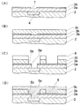
12 …半導体基板
14 …第1層間膜
16 …第2層間膜
18 …導電部
20 …コンタクトホール
22 …配線溝
24 …メタル配線
Claims (4)
- 第1の層間膜、
前記第1の層間膜に形成されたコンタクトホール、
前記第1の層間膜の表面に形成された第2の層間膜、および
前記第2の層間膜をエッチングすることによって形成されて前記コンタクトホ
ールに連通する配線溝を備える、半導体装置であって、
前記第1の層間膜は前記エッチングにおける前記第2の層間膜のエッチングレ
ートより小さいエッチングレートを有する、半導体装置。 - 前記第1の層間膜は窒化膜である、請求項1記載の半導体装置。
- 半導体基板上に第1の層間膜を積層し、
前記第1の層間膜の表面に第2の層間膜を積層し、
前記第1の層間膜をエッチングストッパとして利用して前記第2の層間膜をエ
ッチングして配線溝を形成し、
前記第1の層間膜をエッチングして前記配線溝に連通するコンタクトホールを
形成する、半導体装置の製造方法。 - 半導体基板上に第1の層間膜を積層し、
前記第1の層間膜をエッチングしてコンタクトホールを形成し、
前記第1の層間膜の表面に第2の層間膜を積層し、
前記第1の層間膜をエッチングストッパとして利用して前記第2の層間膜をエ
ッチングして前記コンタクトホールに連通する配線溝を形成する、半導体装置の
製造方法。
Priority Applications (1)
| Application Number | Priority Date | Filing Date | Title |
|---|---|---|---|
| JP2007046498A JP2007142475A (ja) | 2007-02-27 | 2007-02-27 | 半導体装置およびその製造方法 |
Applications Claiming Priority (1)
| Application Number | Priority Date | Filing Date | Title |
|---|---|---|---|
| JP2007046498A JP2007142475A (ja) | 2007-02-27 | 2007-02-27 | 半導体装置およびその製造方法 |
Related Parent Applications (1)
| Application Number | Title | Priority Date | Filing Date |
|---|---|---|---|
| JP10021810A Division JPH11220025A (ja) | 1998-02-03 | 1998-02-03 | 半導体装置およびその製造方法 |
Related Child Applications (1)
| Application Number | Title | Priority Date | Filing Date |
|---|---|---|---|
| JP2011019388A Division JP2011086969A (ja) | 2011-02-01 | 2011-02-01 | 半導体装置およびその製造方法 |
Publications (1)
| Publication Number | Publication Date |
|---|---|
| JP2007142475A true JP2007142475A (ja) | 2007-06-07 |
Family
ID=38204868
Family Applications (1)
| Application Number | Title | Priority Date | Filing Date |
|---|---|---|---|
| JP2007046498A Pending JP2007142475A (ja) | 2007-02-27 | 2007-02-27 | 半導体装置およびその製造方法 |
Country Status (1)
| Country | Link |
|---|---|
| JP (1) | JP2007142475A (ja) |
Cited By (1)
| Publication number | Priority date | Publication date | Assignee | Title |
|---|---|---|---|---|
| JP2011086969A (ja) * | 2011-02-01 | 2011-04-28 | Rohm Co Ltd | 半導体装置およびその製造方法 |
Citations (4)
| Publication number | Priority date | Publication date | Assignee | Title |
|---|---|---|---|---|
| JPH0546983B2 (ja) * | 1985-10-28 | 1993-07-15 | Ibm | |
| JPH06140518A (ja) * | 1992-10-26 | 1994-05-20 | Nippon Steel Corp | 半導体装置の製造方法 |
| JPH0714831A (ja) * | 1993-06-15 | 1995-01-17 | Nec Kyushu Ltd | 半導体装置及びその製造方法 |
| US5705430A (en) * | 1995-06-07 | 1998-01-06 | Advanced Micro Devices, Inc. | Dual damascene with a sacrificial via fill |
-
2007
- 2007-02-27 JP JP2007046498A patent/JP2007142475A/ja active Pending
Patent Citations (4)
| Publication number | Priority date | Publication date | Assignee | Title |
|---|---|---|---|---|
| JPH0546983B2 (ja) * | 1985-10-28 | 1993-07-15 | Ibm | |
| JPH06140518A (ja) * | 1992-10-26 | 1994-05-20 | Nippon Steel Corp | 半導体装置の製造方法 |
| JPH0714831A (ja) * | 1993-06-15 | 1995-01-17 | Nec Kyushu Ltd | 半導体装置及びその製造方法 |
| US5705430A (en) * | 1995-06-07 | 1998-01-06 | Advanced Micro Devices, Inc. | Dual damascene with a sacrificial via fill |
Cited By (1)
| Publication number | Priority date | Publication date | Assignee | Title |
|---|---|---|---|---|
| JP2011086969A (ja) * | 2011-02-01 | 2011-04-28 | Rohm Co Ltd | 半導体装置およびその製造方法 |
Similar Documents
| Publication | Publication Date | Title |
|---|---|---|
| US6800550B2 (en) | Method for forming t-shaped conductive wires of semiconductor device utilizing notching phenomenon | |
| JP2005535124A (ja) | 集積回路におけるコンタクトサイズをサイジングすることによって多層コンタクトを製造するための方法 | |
| JP2012038961A (ja) | 半導体装置及び半導体装置の製造方法 | |
| US7187080B2 (en) | Semiconductor device with a conductive layer including a copper layer with a dopant | |
| KR100442867B1 (ko) | 반도체 소자의 듀얼 다마신 구조 형성방법 | |
| JPWO2007078011A1 (ja) | 多層配線の製造方法と多層配線構造 | |
| JP2006286932A (ja) | 半導体装置の製造方法 | |
| JP2007142475A (ja) | 半導体装置およびその製造方法 | |
| JPH10116904A (ja) | 半導体装置の製造方法 | |
| JPH11220025A (ja) | 半導体装置およびその製造方法 | |
| JP2000183150A (ja) | 半導体装置の製造方法 | |
| JP2011086969A (ja) | 半導体装置およびその製造方法 | |
| JP2000114259A (ja) | 半導体装置における配線の形成方法 | |
| JP2014039059A (ja) | 半導体装置およびその製造方法 | |
| KR101103550B1 (ko) | 반도체 소자의 금속배선 형성방법 | |
| KR100475536B1 (ko) | 반도체 소자의 제조 방법 | |
| JP2007173761A (ja) | 半導体素子の製造方法 | |
| JP2010016236A (ja) | 半導体装置の製造方法 | |
| JP2006351732A (ja) | 半導体装置の製造方法 | |
| JP5288734B2 (ja) | 半導体装置およびその製造方法 | |
| JP2007521630A (ja) | 集積回路におけるコンタクトサイズをサイジングすることによって多層コンタクトを製造するための方法 | |
| KR100850079B1 (ko) | 듀얼 다마신 방법을 이용한 금속 배선 형성 방법 | |
| JP4379245B2 (ja) | 半導体装置の製造方法 | |
| JP2009054879A (ja) | 集積回路の製造方法 | |
| KR100741269B1 (ko) | 반도체 소자의 금속배선 형성 방법 |
Legal Events
| Date | Code | Title | Description |
|---|---|---|---|
| A521 | Written amendment |
Effective date: 20070319 Free format text: JAPANESE INTERMEDIATE CODE: A523 |
|
| A621 | Written request for application examination |
Free format text: JAPANESE INTERMEDIATE CODE: A621 Effective date: 20070319 |
|
| RD04 | Notification of resignation of power of attorney |
Free format text: JAPANESE INTERMEDIATE CODE: A7424 Effective date: 20070822 |
|
| RD04 | Notification of resignation of power of attorney |
Free format text: JAPANESE INTERMEDIATE CODE: A7424 Effective date: 20070731 |
|
| A131 | Notification of reasons for refusal |
Free format text: JAPANESE INTERMEDIATE CODE: A131 Effective date: 20100803 |
|
| A977 | Report on retrieval |
Effective date: 20100805 Free format text: JAPANESE INTERMEDIATE CODE: A971007 |
|
| A521 | Written amendment |
Free format text: JAPANESE INTERMEDIATE CODE: A523 Effective date: 20101004 |
|
| A02 | Decision of refusal |
Free format text: JAPANESE INTERMEDIATE CODE: A02 Effective date: 20101102 |
|
| A521 | Written amendment |
Free format text: JAPANESE INTERMEDIATE CODE: A523 Effective date: 20110201 |
|
| A911 | Transfer of reconsideration by examiner before appeal (zenchi) |
Effective date: 20110208 Free format text: JAPANESE INTERMEDIATE CODE: A911 |