JP2007201879A - 差動信号受信回路 - Google Patents
差動信号受信回路 Download PDFInfo
- Publication number
- JP2007201879A JP2007201879A JP2006018842A JP2006018842A JP2007201879A JP 2007201879 A JP2007201879 A JP 2007201879A JP 2006018842 A JP2006018842 A JP 2006018842A JP 2006018842 A JP2006018842 A JP 2006018842A JP 2007201879 A JP2007201879 A JP 2007201879A
- Authority
- JP
- Japan
- Prior art keywords
- differential signal
- signal
- circuit
- receiving circuit
- enhancement type
- Prior art date
- Legal status (The legal status is an assumption and is not a legal conclusion. Google has not performed a legal analysis and makes no representation as to the accuracy of the status listed.)
- Granted
Links
- 238000007493 shaping process Methods 0.000 claims abstract description 36
- 238000010586 diagram Methods 0.000 description 15
- 239000004973 liquid crystal related substance Substances 0.000 description 8
- 238000006243 chemical reaction Methods 0.000 description 7
- 230000003321 amplification Effects 0.000 description 5
- 238000003199 nucleic acid amplification method Methods 0.000 description 5
- 230000007423 decrease Effects 0.000 description 4
- 230000005540 biological transmission Effects 0.000 description 3
- 239000003086 colorant Substances 0.000 description 2
- 230000011664 signaling Effects 0.000 description 2
- 238000004519 manufacturing process Methods 0.000 description 1
- 239000011159 matrix material Substances 0.000 description 1
- 239000010409 thin film Substances 0.000 description 1
Images


Classifications
-
- H—ELECTRICITY
- H03—ELECTRONIC CIRCUITRY
- H03F—AMPLIFIERS
- H03F3/00—Amplifiers with only discharge tubes or only semiconductor devices as amplifying elements
- H03F3/45—Differential amplifiers
- H03F3/45071—Differential amplifiers with semiconductor devices only
- H03F3/45076—Differential amplifiers with semiconductor devices only characterised by the way of implementation of the active amplifying circuit in the differential amplifier
- H03F3/45179—Differential amplifiers with semiconductor devices only characterised by the way of implementation of the active amplifying circuit in the differential amplifier using MOSFET transistors as the active amplifying circuit
- H03F3/45183—Long tailed pairs
-
- H—ELECTRICITY
- H03—ELECTRONIC CIRCUITRY
- H03F—AMPLIFIERS
- H03F2200/00—Indexing scheme relating to amplifiers
- H03F2200/408—Indexing scheme relating to amplifiers the output amplifying stage of an amplifier comprising three power stages
-
- H—ELECTRICITY
- H03—ELECTRONIC CIRCUITRY
- H03F—AMPLIFIERS
- H03F2203/00—Indexing scheme relating to amplifiers with only discharge tubes or only semiconductor devices as amplifying elements covered by H03F3/00
- H03F2203/45—Indexing scheme relating to differential amplifiers
- H03F2203/45612—Indexing scheme relating to differential amplifiers the IC comprising one or more input source followers as input stages in the IC
-
- H—ELECTRICITY
- H03—ELECTRONIC CIRCUITRY
- H03F—AMPLIFIERS
- H03F2203/00—Indexing scheme relating to amplifiers with only discharge tubes or only semiconductor devices as amplifying elements covered by H03F3/00
- H03F2203/45—Indexing scheme relating to differential amplifiers
- H03F2203/45652—Indexing scheme relating to differential amplifiers the LC comprising one or more further dif amp stages, either identical to the dif amp or not, in cascade
-
- H—ELECTRICITY
- H03—ELECTRONIC CIRCUITRY
- H03F—AMPLIFIERS
- H03F2203/00—Indexing scheme relating to amplifiers with only discharge tubes or only semiconductor devices as amplifying elements covered by H03F3/00
- H03F2203/45—Indexing scheme relating to differential amplifiers
- H03F2203/45696—Indexing scheme relating to differential amplifiers the LC comprising more than two resistors
Landscapes
- Engineering & Computer Science (AREA)
- Power Engineering (AREA)
- Amplifiers (AREA)
- Manipulation Of Pulses (AREA)
- Logic Circuits (AREA)
Abstract
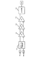
【解決手段】本発明にかかる差動信号受信回路は、入力される差動信号に応じて、第1の電源電位と第1の電位差を有する上限値と、上限値と第2の電位差を有する下限値とを選択的に第1、第2の出力端子から出力する波形整形回路10と、第1、第2の出力端子の電圧を比較し、第1の電源電位と略同一の電圧と第2の電源と略同一の電圧とのいずれか一方を出力する増幅回路11とを有するものである。
【選択図】図1
Description
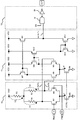
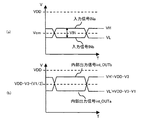
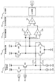
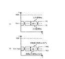
以下図面を参照して本発明の実施の形態について説明する。実施の形態1にかかる差動信号受信回路1は、小振幅の差動信号を入力し、大振幅のシングルエンド信号を出力する。例えば、入力される差動信号の振幅は、0.2V(ロウレベル:0.8V、ハイレベル:1.0V)、あるいは0.6V(ロウレベル:0.2V、ハイレベル:0.8V)程度である。また、出力されるシングルエンド信号は、例えば第1の電源(例えば、電源電位VDD)と第2の電源(例えば、接地電位GND)との電位差の振幅を有する。実施の形態1にかかる差動信号受信回路1の回路図を図1に示す。
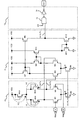
実施の形態1にかかる差動信号受信回路1は、波形整形回路10の第1の電位差設定素子として抵抗R3を用いていたが、実施の形態2にかかる差動信号受信回路2の波形整形回路20の第1の電位差設定素子は、ダイオード接続されたNchエンハンスメント型トランジスタM13を用いる。実施の形態2にかかる差動信号受信回路2の回路図を図3に示す。図3において、実施の形態1と実質的に同じ要素については、実施の形態1と同じ符号を付して、以下で行う説明を省略する。
実施の形態2にかかる差動信号受信回路1は、波形整形回路20の第2の電位差設定素子として抵抗R1、R2を用いていたが、実施の形態3にかかる差動信号受信回路3の波形整形回路30の第2の電位差設定素子は、ダイオード接続されたNchエンハンスメント型トランジスタM14、Nchエンハンスメント型トランジスタ15を用いる。実施の形態3にかかる差動信号受信回路3の回路図を図4に示す。図4において、実施の形態2と実質的に同じ要素については、実施の形態2と同じ符号を付して、以下で行う説明を省略する。
10、20、30 波形整形回路
11 増幅回路
12 出力制御回路
13 NAND回路
14 インバータ回路
A、B 入力端子
OUT 出力端子
EN 出力制御信号
INa、INb 差動信号
int_OUTa、int_OUTb、int_OUTc 内部出力信号
M1、M2 Nchデプレッション型トランジスタ
M4〜M6、M11、M12、M13〜M15 Nchエンハンスメント型トランジスタ
M7〜M10 Pchエンハンスメント型トランジスタ
R1〜R3 抵抗
Claims (6)
- 入力される差動信号に応じて、第1の電源電位と第1の電位差を有する上限値と、前記上限値と第2の電位差を有する下限値とを選択的に第1、第2の出力端子から出力する波形整形回路と、
前記第1、第2の出力端子の電圧を比較し、前記第1の電源電位と略同一の電圧と第2の電源と略同一の電圧とのいずれか一方を出力する増幅回路とを有する差動信号受信回路。 - 前記波形整形回路は、前記第1の電位差を設定する第1の電位差設定素子と、前記第2の電位差を設定する第2の電位差設定素子と、前記差動信号を受信する複数のデプレッション型トランジスタと、前記複数のデプレッション型トランジスタに電流を供給する電流源とを有していることを特徴とする請求項1に記載の差動信号受信回路。
- 前記第1、第2の電位差設定素子のうち少なくとも一方は、抵抗素子であることを特徴とする請求項2に記載の差動信号受信回路。
- 前記第1、第2の電位差は、前記電流源が出力する電流と、前記抵抗素子に基づいて設定されることを特徴とする請求項3に記載の差動信号受信回路。
- 前記第1、第2の電位差設定素子のうち少なくとも一方は、ダイオード接続されたトランジスタであることを特徴とする請求項2に記載の差動信号受信回路。
- 前記第1、第2の電位差は、前記ダイオード接続されたトランジスタの閾値電圧に基づいて設定されることを特徴とする請求項5に記載の差動信号受信回路。
Priority Applications (3)
| Application Number | Priority Date | Filing Date | Title |
|---|---|---|---|
| JP2006018842A JP4851192B2 (ja) | 2006-01-27 | 2006-01-27 | 差動信号受信回路 |
| US11/656,533 US7675323B2 (en) | 2006-01-27 | 2007-01-23 | Differential signal receiver |
| CN200710008349XA CN101009478B (zh) | 2006-01-27 | 2007-01-29 | 差分信号接收器 |
Applications Claiming Priority (1)
| Application Number | Priority Date | Filing Date | Title |
|---|---|---|---|
| JP2006018842A JP4851192B2 (ja) | 2006-01-27 | 2006-01-27 | 差動信号受信回路 |
Publications (2)
| Publication Number | Publication Date |
|---|---|
| JP2007201879A true JP2007201879A (ja) | 2007-08-09 |
| JP4851192B2 JP4851192B2 (ja) | 2012-01-11 |
Family
ID=38367746
Family Applications (1)
| Application Number | Title | Priority Date | Filing Date |
|---|---|---|---|
| JP2006018842A Expired - Fee Related JP4851192B2 (ja) | 2006-01-27 | 2006-01-27 | 差動信号受信回路 |
Country Status (3)
| Country | Link |
|---|---|
| US (1) | US7675323B2 (ja) |
| JP (1) | JP4851192B2 (ja) |
| CN (1) | CN101009478B (ja) |
Cited By (2)
| Publication number | Priority date | Publication date | Assignee | Title |
|---|---|---|---|---|
| JP2011071979A (ja) * | 2009-09-28 | 2011-04-07 | Samsung Electronics Co Ltd | 信号入力回路及びそれを含む半導体装置 |
| JP2019009548A (ja) * | 2017-06-22 | 2019-01-17 | ローム株式会社 | オペアンプ及びそれを用いたdc/dcコンバータ |
Families Citing this family (6)
| Publication number | Priority date | Publication date | Assignee | Title |
|---|---|---|---|---|
| CN102420602B (zh) * | 2011-12-09 | 2014-05-28 | 无锡中星微电子有限公司 | 一种电源转换器及差分电路 |
| US8829941B2 (en) * | 2011-12-10 | 2014-09-09 | Advanced Micro Devices, Inc. | Low-power high-gain multistage comparator circuit |
| EP3113359B1 (en) * | 2013-11-28 | 2019-01-02 | ams AG | Amplifier arrangement |
| US9318598B2 (en) * | 2014-05-30 | 2016-04-19 | Texas Instruments Incorporated | Trench MOSFET having reduced gate charge |
| CN105576967B (zh) * | 2014-10-11 | 2018-07-24 | 中芯国际集成电路制造(上海)有限公司 | 升压转换电路 |
| CN104901683B (zh) * | 2015-04-28 | 2017-10-20 | 灿芯半导体(上海)有限公司 | 信号接收电路 |
Citations (6)
| Publication number | Priority date | Publication date | Assignee | Title |
|---|---|---|---|---|
| JPS63284912A (ja) * | 1987-04-24 | 1988-11-22 | アメリカン テレフオン アンド テレグラフ カムパニー | 可変オフセットを有する差動集積回路 |
| JPH01223807A (ja) * | 1988-03-02 | 1989-09-06 | Matsushita Electric Ind Co Ltd | 出力回路 |
| JPH05304426A (ja) * | 1991-07-04 | 1993-11-16 | Ricoh Co Ltd | 半導体装置 |
| JPH07226557A (ja) * | 1994-02-15 | 1995-08-22 | Hitachi Ltd | 電子回路およびこれを用いた半導体装置 |
| JPH1075133A (ja) * | 1996-08-29 | 1998-03-17 | Fujitsu Ltd | オペアンプ回路 |
| JP2003264437A (ja) * | 2002-03-12 | 2003-09-19 | Oki Electric Ind Co Ltd | アナログ加減算回路、光受信回路、光送信回路、自動利得制御増幅回路、自動周波数特性補償増幅回路、リミット増幅回路 |
Family Cites Families (11)
| Publication number | Priority date | Publication date | Assignee | Title |
|---|---|---|---|---|
| US4918336A (en) * | 1987-05-19 | 1990-04-17 | Gazelle Microcircuits, Inc. | Capacitor coupled push pull logic circuit |
| JP2798020B2 (ja) * | 1995-10-25 | 1998-09-17 | 日本電気株式会社 | 半導体集積回路 |
| JP3157746B2 (ja) * | 1997-06-30 | 2001-04-16 | 日本電気アイシーマイコンシステム株式会社 | 定電流回路 |
| KR100290285B1 (ko) * | 1999-01-13 | 2001-05-15 | 윤종용 | 프리스케일러의 입력 버퍼 |
| KR100393226B1 (ko) * | 2001-07-04 | 2003-07-31 | 삼성전자주식회사 | 온도변화에 따라 내부 기준전압 값을 조절할 수 있는 내부기준전압 생성회로 및 이를 구비하는 내부 공급전압생성회로 |
| JP2003198265A (ja) | 2001-12-25 | 2003-07-11 | Seiko Epson Corp | 差動信号受信回路 |
| KR100480916B1 (ko) * | 2002-10-30 | 2005-04-07 | 주식회사 하이닉스반도체 | 전류 소모를 줄인 입력 버퍼 회로 |
| US7061273B2 (en) * | 2003-06-06 | 2006-06-13 | Rambus Inc. | Method and apparatus for multi-mode driver |
| JP3827654B2 (ja) * | 2003-06-23 | 2006-09-27 | 株式会社 沖マイクロデザイン | 演算増幅器 |
| KR100616501B1 (ko) * | 2004-07-27 | 2006-08-25 | 주식회사 하이닉스반도체 | 리시버 |
| US7446576B2 (en) * | 2005-09-30 | 2008-11-04 | Slt Logics, Llc | Output driver with slew rate control |
-
2006
- 2006-01-27 JP JP2006018842A patent/JP4851192B2/ja not_active Expired - Fee Related
-
2007
- 2007-01-23 US US11/656,533 patent/US7675323B2/en not_active Expired - Fee Related
- 2007-01-29 CN CN200710008349XA patent/CN101009478B/zh not_active Expired - Fee Related
Patent Citations (6)
| Publication number | Priority date | Publication date | Assignee | Title |
|---|---|---|---|---|
| JPS63284912A (ja) * | 1987-04-24 | 1988-11-22 | アメリカン テレフオン アンド テレグラフ カムパニー | 可変オフセットを有する差動集積回路 |
| JPH01223807A (ja) * | 1988-03-02 | 1989-09-06 | Matsushita Electric Ind Co Ltd | 出力回路 |
| JPH05304426A (ja) * | 1991-07-04 | 1993-11-16 | Ricoh Co Ltd | 半導体装置 |
| JPH07226557A (ja) * | 1994-02-15 | 1995-08-22 | Hitachi Ltd | 電子回路およびこれを用いた半導体装置 |
| JPH1075133A (ja) * | 1996-08-29 | 1998-03-17 | Fujitsu Ltd | オペアンプ回路 |
| JP2003264437A (ja) * | 2002-03-12 | 2003-09-19 | Oki Electric Ind Co Ltd | アナログ加減算回路、光受信回路、光送信回路、自動利得制御増幅回路、自動周波数特性補償増幅回路、リミット増幅回路 |
Cited By (2)
| Publication number | Priority date | Publication date | Assignee | Title |
|---|---|---|---|---|
| JP2011071979A (ja) * | 2009-09-28 | 2011-04-07 | Samsung Electronics Co Ltd | 信号入力回路及びそれを含む半導体装置 |
| JP2019009548A (ja) * | 2017-06-22 | 2019-01-17 | ローム株式会社 | オペアンプ及びそれを用いたdc/dcコンバータ |
Also Published As
| Publication number | Publication date |
|---|---|
| CN101009478B (zh) | 2010-10-06 |
| CN101009478A (zh) | 2007-08-01 |
| US7675323B2 (en) | 2010-03-09 |
| US20070188230A1 (en) | 2007-08-16 |
| JP4851192B2 (ja) | 2012-01-11 |
Similar Documents
| Publication | Publication Date | Title |
|---|---|---|
| US10650770B2 (en) | Output circuit and data driver of liquid crystal display device | |
| US6392485B1 (en) | High slew rate differential amplifier circuit | |
| CN101178883B (zh) | 数据驱动器及显示装置 | |
| US8368673B2 (en) | Output buffer and source driver using the same | |
| JP4836469B2 (ja) | 階調電圧発生回路 | |
| JP4103468B2 (ja) | 差動回路と増幅回路及び該増幅回路を用いた表示装置 | |
| JP4475309B2 (ja) | コンパレータ | |
| JP2009152944A (ja) | 出力ドライバ回路 | |
| US7907136B2 (en) | Voltage generation circuit | |
| CN101944341A (zh) | 液晶显示驱动器和液晶显示装置 | |
| JP2010041392A (ja) | Ab級増幅回路、及び表示装置 | |
| US7675323B2 (en) | Differential signal receiver | |
| US7038502B2 (en) | LVDS driver circuit and driver circuit | |
| US7646371B2 (en) | Driver circuit, electro-optical device, and electronic instrument | |
| JP2010226592A (ja) | 演算増幅器 | |
| US20100321360A1 (en) | Differential signal receiving circuit and display apparatus | |
| JP2008032812A (ja) | 出力駆動装置および表示装置 | |
| JP2007086391A (ja) | 階調電圧発生回路 | |
| JP2002353792A (ja) | 駆動回路および表示装置 | |
| CN101416230B (zh) | 显示装置 | |
| US20090167666A1 (en) | LCD Driver IC and Method for Operating the Same | |
| JP5375422B2 (ja) | 半導体電子回路、発振回路およびフリップフロップ回路 | |
| JP3209967B2 (ja) | 電流セル及びこれを用いたディジタル/アナログ変換器 | |
| JP2005311790A (ja) | 信号レベル変換回路および該回路を用いた液晶表示装置 | |
| JP5021501B2 (ja) | 出力ドライバ回路 |
Legal Events
| Date | Code | Title | Description |
|---|---|---|---|
| A621 | Written request for application examination |
Free format text: JAPANESE INTERMEDIATE CODE: A621 Effective date: 20081215 |
|
| A977 | Report on retrieval |
Free format text: JAPANESE INTERMEDIATE CODE: A971007 Effective date: 20101018 |
|
| A131 | Notification of reasons for refusal |
Free format text: JAPANESE INTERMEDIATE CODE: A131 Effective date: 20101026 |
|
| A521 | Written amendment |
Free format text: JAPANESE INTERMEDIATE CODE: A523 Effective date: 20101224 |
|
| A131 | Notification of reasons for refusal |
Free format text: JAPANESE INTERMEDIATE CODE: A131 Effective date: 20110517 |
|
| A521 | Written amendment |
Free format text: JAPANESE INTERMEDIATE CODE: A523 Effective date: 20110715 |
|
| TRDD | Decision of grant or rejection written | ||
| A01 | Written decision to grant a patent or to grant a registration (utility model) |
Free format text: JAPANESE INTERMEDIATE CODE: A01 Effective date: 20111018 |
|
| A01 | Written decision to grant a patent or to grant a registration (utility model) |
Free format text: JAPANESE INTERMEDIATE CODE: A01 |
|
| A61 | First payment of annual fees (during grant procedure) |
Free format text: JAPANESE INTERMEDIATE CODE: A61 Effective date: 20111020 |
|
| R150 | Certificate of patent or registration of utility model |
Free format text: JAPANESE INTERMEDIATE CODE: R150 |
|
| FPAY | Renewal fee payment (event date is renewal date of database) |
Free format text: PAYMENT UNTIL: 20141028 Year of fee payment: 3 |
|
| S531 | Written request for registration of change of domicile |
Free format text: JAPANESE INTERMEDIATE CODE: R313531 |
|
| R350 | Written notification of registration of transfer |
Free format text: JAPANESE INTERMEDIATE CODE: R350 |
|
| LAPS | Cancellation because of no payment of annual fees |