JP2007258755A - 半導体装置 - Google Patents
半導体装置 Download PDFInfo
- Publication number
- JP2007258755A JP2007258755A JP2007168695A JP2007168695A JP2007258755A JP 2007258755 A JP2007258755 A JP 2007258755A JP 2007168695 A JP2007168695 A JP 2007168695A JP 2007168695 A JP2007168695 A JP 2007168695A JP 2007258755 A JP2007258755 A JP 2007258755A
- Authority
- JP
- Japan
- Prior art keywords
- functional
- substrate
- semiconductor device
- bumps
- region
- Prior art date
- Legal status (The legal status is an assumption and is not a legal conclusion. Google has not performed a legal analysis and makes no representation as to the accuracy of the status listed.)
- Granted
Links
Images




Classifications
-
- H—ELECTRICITY
- H10—SEMICONDUCTOR DEVICES; ELECTRIC SOLID-STATE DEVICES NOT OTHERWISE PROVIDED FOR
- H10W—GENERIC PACKAGES, INTERCONNECTIONS, CONNECTORS OR OTHER CONSTRUCTIONAL DETAILS OF DEVICES COVERED BY CLASS H10
- H10W90/00—Package configurations
- H10W90/701—Package configurations characterised by the relative positions of pads or connectors relative to package parts
- H10W90/721—Package configurations characterised by the relative positions of pads or connectors relative to package parts of bump connectors
- H10W90/724—Package configurations characterised by the relative positions of pads or connectors relative to package parts of bump connectors between a chip and a stacked insulating package substrate, interposer or RDL
Landscapes
- Wire Bonding (AREA)
Abstract
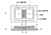
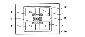
【解決手段】本発明は、記憶素子からなり複数に領域が分割された第1の機能領域1と、外部との信号入出力を行う複数のバンプBを有し第1の機能領域1間にも領域を有する第2の機能領域2とが同一基板に設けられている半導体の基板10と、この基板10の上記複数のバンプBと直接接続された外部基板20とを有する半導体装置であって、前記半導体の基板10を平面視した場合、第1の機能領域1間の第2の機能領域2に、上記複数のバンプBが形成されているものである。
【選択図】図1
Description
Claims (4)
- 記憶素子からなり複数に領域が分割された第1の機能領域と、外部との信号入出力を行う複数のバンプを有し上記第1の機能領域間にも領域を有する第2の機能領域とが同一基板に設けられている半導体基板と、
上記半導体基板の上記複数のバンプと直接接続された外部基板とを備える半導体装置であって、
前記半導体基板を平面視した場合、前記第1の機能領域間の前記第2の機能領域に、上記複数のバンプが形成されている
ことを特徴とする半導体装置。 - 前記第2の機能領域には、駆動回路もしくは信号処理回路を有することを特徴とする請求項1記載の半導体装置。
- 前記第2の機能領域における耐加圧力は前記第1の機能領域における耐加圧力より大きい
ことを特徴とする請求項1記載の半導体装置。 - 記憶素子からなる第1の機能領域と、外部との信号入出力を行う複数のバンプを有し上記第1の機能領域に囲まれる領域を有する第2の機能領域とが同一基板に設けられている半導体基板と、
上記半導体基板の上記複数のバンプと直接接続された外部基板とを備える半導体装置であって、
前記半導体基板を平面視した場合、前記第1の機能領域に囲まれている前記第2の機能領域に、上記複数のバンプが形成されている
ことを特徴とする半導体装置。
Priority Applications (1)
| Application Number | Priority Date | Filing Date | Title |
|---|---|---|---|
| JP2007168695A JP4618275B2 (ja) | 2007-06-27 | 2007-06-27 | 半導体装置 |
Applications Claiming Priority (1)
| Application Number | Priority Date | Filing Date | Title |
|---|---|---|---|
| JP2007168695A JP4618275B2 (ja) | 2007-06-27 | 2007-06-27 | 半導体装置 |
Related Parent Applications (1)
| Application Number | Title | Priority Date | Filing Date |
|---|---|---|---|
| JP2003040730A Division JP2004265940A (ja) | 2003-02-19 | 2003-02-19 | 半導体装置 |
Publications (2)
| Publication Number | Publication Date |
|---|---|
| JP2007258755A true JP2007258755A (ja) | 2007-10-04 |
| JP4618275B2 JP4618275B2 (ja) | 2011-01-26 |
Family
ID=38632609
Family Applications (1)
| Application Number | Title | Priority Date | Filing Date |
|---|---|---|---|
| JP2007168695A Expired - Fee Related JP4618275B2 (ja) | 2007-06-27 | 2007-06-27 | 半導体装置 |
Country Status (1)
| Country | Link |
|---|---|
| JP (1) | JP4618275B2 (ja) |
Citations (4)
| Publication number | Priority date | Publication date | Assignee | Title |
|---|---|---|---|---|
| JPH05343634A (ja) * | 1992-06-06 | 1993-12-24 | Hitachi Ltd | 半導体記憶装置 |
| JPH1131716A (ja) * | 1997-07-11 | 1999-02-02 | Hitachi Ltd | 半導体装置の製造方法及び半導体チップ |
| JPH11288977A (ja) * | 1998-03-31 | 1999-10-19 | Nippon Steel Corp | 複数チップ混載型半導体装置 |
| JP2000188381A (ja) * | 1998-12-22 | 2000-07-04 | Toshiba Corp | 半導体記憶装置 |
-
2007
- 2007-06-27 JP JP2007168695A patent/JP4618275B2/ja not_active Expired - Fee Related
Patent Citations (4)
| Publication number | Priority date | Publication date | Assignee | Title |
|---|---|---|---|---|
| JPH05343634A (ja) * | 1992-06-06 | 1993-12-24 | Hitachi Ltd | 半導体記憶装置 |
| JPH1131716A (ja) * | 1997-07-11 | 1999-02-02 | Hitachi Ltd | 半導体装置の製造方法及び半導体チップ |
| JPH11288977A (ja) * | 1998-03-31 | 1999-10-19 | Nippon Steel Corp | 複数チップ混載型半導体装置 |
| JP2000188381A (ja) * | 1998-12-22 | 2000-07-04 | Toshiba Corp | 半導体記憶装置 |
Also Published As
| Publication number | Publication date |
|---|---|
| JP4618275B2 (ja) | 2011-01-26 |
Similar Documents
| Publication | Publication Date | Title |
|---|---|---|
| US6836007B2 (en) | Semiconductor package including stacked semiconductor chips | |
| US6242814B1 (en) | Universal I/O pad structure for in-line or staggered wire bonding or arrayed flip-chip assembly | |
| KR20040014156A (ko) | 반도체장치 | |
| JP2009164195A (ja) | 半導体チップ | |
| JP2010010492A (ja) | 半導体装置および半導体集積回路 | |
| JP7093020B2 (ja) | 半導体集積回路装置 | |
| JP2005268670A (ja) | 半導体装置 | |
| KR970072228A (ko) | 반도체 집적회로장치 | |
| USRE44699E1 (en) | Semiconductor integrated circuit having pads layout for increasing signal integrity and reducing chip size | |
| JP2006066898A (ja) | 半導体装置 | |
| JP6875642B2 (ja) | 半導体チップおよびこれを備えた半導体装置 | |
| US6720636B2 (en) | Semiconductor device with a staggered pad arrangement | |
| JP4738996B2 (ja) | 半導体装置 | |
| JP4618275B2 (ja) | 半導体装置 | |
| JP2004265940A (ja) | 半導体装置 | |
| JP4754201B2 (ja) | 半導体装置 | |
| JPH061801B2 (ja) | リ−ドフレ−ム | |
| JPH04199563A (ja) | 半導体集積回路用パッケージ | |
| JP4708865B2 (ja) | 半導体装置 | |
| JP2007103792A (ja) | 半導体装置 | |
| US20100059874A1 (en) | Semiconductor chip capable of increased number of pads in limited region and semiconductor package using the same | |
| JP2006286688A (ja) | 半導体装置 | |
| JP2005032871A (ja) | 半導体装置 | |
| JP2005268533A (ja) | 積層型半導体装置 | |
| JP2005268534A (ja) | 半導体チップおよび積層型半導体装置 |
Legal Events
| Date | Code | Title | Description |
|---|---|---|---|
| A621 | Written request for application examination |
Free format text: JAPANESE INTERMEDIATE CODE: A621 Effective date: 20070627 |
|
| RD02 | Notification of acceptance of power of attorney |
Free format text: JAPANESE INTERMEDIATE CODE: A7422 Effective date: 20091007 |
|
| RD04 | Notification of resignation of power of attorney |
Free format text: JAPANESE INTERMEDIATE CODE: A7424 Effective date: 20091019 |
|
| A131 | Notification of reasons for refusal |
Free format text: JAPANESE INTERMEDIATE CODE: A131 Effective date: 20100427 |
|
| A521 | Request for written amendment filed |
Free format text: JAPANESE INTERMEDIATE CODE: A523 Effective date: 20100621 |
|
| A131 | Notification of reasons for refusal |
Free format text: JAPANESE INTERMEDIATE CODE: A131 Effective date: 20100713 |
|
| A521 | Request for written amendment filed |
Free format text: JAPANESE INTERMEDIATE CODE: A523 Effective date: 20100903 |
|
| TRDD | Decision of grant or rejection written | ||
| A01 | Written decision to grant a patent or to grant a registration (utility model) |
Free format text: JAPANESE INTERMEDIATE CODE: A01 Effective date: 20100928 |
|
| A01 | Written decision to grant a patent or to grant a registration (utility model) |
Free format text: JAPANESE INTERMEDIATE CODE: A01 |
|
| A61 | First payment of annual fees (during grant procedure) |
Free format text: JAPANESE INTERMEDIATE CODE: A61 Effective date: 20101011 |
|
| FPAY | Renewal fee payment (event date is renewal date of database) |
Free format text: PAYMENT UNTIL: 20131105 Year of fee payment: 3 |
|
| FPAY | Renewal fee payment (event date is renewal date of database) |
Free format text: PAYMENT UNTIL: 20131105 Year of fee payment: 3 |
|
| LAPS | Cancellation because of no payment of annual fees |