JP2007266594A - 強化リソグラフィパターニング方法およびシステム - Google Patents
強化リソグラフィパターニング方法およびシステム Download PDFInfo
- Publication number
- JP2007266594A JP2007266594A JP2007048814A JP2007048814A JP2007266594A JP 2007266594 A JP2007266594 A JP 2007266594A JP 2007048814 A JP2007048814 A JP 2007048814A JP 2007048814 A JP2007048814 A JP 2007048814A JP 2007266594 A JP2007266594 A JP 2007266594A
- Authority
- JP
- Japan
- Prior art keywords
- hard mask
- radiation beam
- substrate
- patterned
- mask layer
- Prior art date
- Legal status (The legal status is an assumption and is not a legal conclusion. Google has not performed a legal analysis and makes no representation as to the accuracy of the status listed.)
- Granted
Links
Images

Classifications
-
- G—PHYSICS
- G03—PHOTOGRAPHY; CINEMATOGRAPHY; ANALOGOUS TECHNIQUES USING WAVES OTHER THAN OPTICAL WAVES; ELECTROGRAPHY; HOLOGRAPHY
- G03F—PHOTOMECHANICAL PRODUCTION OF TEXTURED OR PATTERNED SURFACES, e.g. FOR PRINTING, FOR PROCESSING OF SEMICONDUCTOR DEVICES; MATERIALS THEREFOR; ORIGINALS THEREFOR; APPARATUS SPECIALLY ADAPTED THEREFOR
- G03F7/00—Photomechanical, e.g. photolithographic, production of textured or patterned surfaces, e.g. printing surfaces; Materials therefor, e.g. comprising photoresists; Apparatus specially adapted therefor
- G03F7/70—Microphotolithographic exposure; Apparatus therefor
- G03F7/70425—Imaging strategies, e.g. for increasing throughput or resolution, printing product fields larger than the image field or compensating lithography- or non-lithography errors, e.g. proximity correction, mix-and-match, stitching or double patterning
- G03F7/70466—Multiple exposures, e.g. combination of fine and coarse exposures, double patterning or multiple exposures for printing a single feature
-
- G—PHYSICS
- G03—PHOTOGRAPHY; CINEMATOGRAPHY; ANALOGOUS TECHNIQUES USING WAVES OTHER THAN OPTICAL WAVES; ELECTROGRAPHY; HOLOGRAPHY
- G03F—PHOTOMECHANICAL PRODUCTION OF TEXTURED OR PATTERNED SURFACES, e.g. FOR PRINTING, FOR PROCESSING OF SEMICONDUCTOR DEVICES; MATERIALS THEREFOR; ORIGINALS THEREFOR; APPARATUS SPECIALLY ADAPTED THEREFOR
- G03F7/00—Photomechanical, e.g. photolithographic, production of textured or patterned surfaces, e.g. printing surfaces; Materials therefor, e.g. comprising photoresists; Apparatus specially adapted therefor
- G03F7/70—Microphotolithographic exposure; Apparatus therefor
- G03F7/70008—Production of exposure light, i.e. light sources
- G03F7/70025—Production of exposure light, i.e. light sources by lasers
Landscapes
- Physics & Mathematics (AREA)
- General Physics & Mathematics (AREA)
- Engineering & Computer Science (AREA)
- Optics & Photonics (AREA)
- Plasma & Fusion (AREA)
- Exposure And Positioning Against Photoresist Photosensitive Materials (AREA)
- Exposure Of Semiconductors, Excluding Electron Or Ion Beam Exposure (AREA)
- Preparing Plates And Mask In Photomechanical Process (AREA)
Abstract
【解決手段】炭素系ハードマスクを用いた二重パターニングシステムおよびプロセス。この二重パターニングシステムは、単一露光に基づいてハードマスクにプリント可能な最小間隔よりも小さいフィーチャ間隔で、1回のハードマスクエッチング工程においてハードマスクフィーチャを形成する手段を提供する。
【選択図】 図4
Description
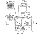
− 投影放射ビームPB(例えば、紫外光(UV)または極端紫外光(EUV))を供給する照明システムIL。特にこの場合、放射システムは放射ソースSOを含む。
− パターニングデバイスMA(例えば、マスク)を支持する第1の支持構造体MT(例えば、マスクテーブル)であって、かつ投影システムPLに対してパターニングデバイスを正確に位置付ける第1位置決め装置(図示されていない)に連結されている、第1の支持構造体MT。
− 基板W(例えば、レジストコートシリコンウェーハ)を保持する第2の支持構造体WT(例えば、ウェーハテーブル)であって、かつ投影システムPLに対して基板を正確に位置付けるように構成された第2位置決め装置PWに連結されている、第2の支持構造体WT。
− パターニングデバイスMAによって放射ビームPBに付けられたパターンを基板Wのターゲット部分C(例えば、1つ以上のダイを含む)上に投影する投影システムPL(例えば、反射投影レンズ)。
Claims (27)
- 基板上に設けられたハードマスク層に向けてパターン付き放射ビームを供給する工程と、
前記ハードマスク層の第1の部分のエッチング特性を強化するのに十分である、前記パターン付き放射ビームからの第1の放射照射量により、前記ハードマスク層の前記第1の部分を露光する工程と、
前記ハードマスク層の前記第1の部分と異なる第2の部分のエッチング特性を強化するのに十分である、前記パターン付き放射ビームからの第2の放射照射量により、前記ハードマスク層の前記第2の部分を露光する工程と、
前記第1の部分および第2の部分を実質的に除去し、かつ前記ハードマスク層のうちの前記第1の部分および第2の部分以外の部分が実質的にそのままの状態となるように、前記ハードマスク層にエッチングプロセスを施す工程と
を備える、パターン転写方法。 - 前記ハードマスク層は、前記放射ビームに露光される前に、多量のダイヤモンド状炭素を有するアモルファス炭素である、請求項1に記載の方法。
- 前記パターン付き放射ビームは、エキシマレーザから発生される248nm、193nm、および157nmのUV放射線の一つを含む、請求項2に記載の方法。
- 前記第1の照射量と前記第2の照射量はほぼ同じである、請求項2に記載の方法。
- 前記第1の照射量と前記第2の照射量はそれぞれ、前記第1の部分および前記第2の部分のそれぞれを実質的に黒鉛化するのに十分である、請求項2に記載の方法。
- 前記エッチングプロセスは、O2反応性イオンエッチングプロセスであり、前記ハードマスク層の非照射部分に対する照射部分のエッチング速度比は約2よりも大きい、請求項2に記載の方法。
- 前記第1の部分を露光した後であって前記第2の部分を露光する前に、水平変位量にわたって前記基板と前記パターン付き放射ビームを相対変位させる工程をさらに備える、請求項1に記載の方法。
- 前記パターン付き放射ビームは、単一露光でハードマスク上にプリント可能な最小フィーチャピッチを有し、前記水平変位量は当該最小フィーチャピッチよりも小さい、請求項7に記載の方法。
- 前記水平変位量は、前記最小フィーチャピッチの約半分である、請求項8に記載の方法。
- 前記第1の部分を露光した後であって前記第2の部分を露光する前に、水平変位量にわたって前記基板と前記パターン付き放射ビームを相対変位させる工程をさらに備え、
前記パターン付き放射ビームは、単一露光でハードマスク上にプリント可能な最小フィーチャピッチを有し、前記水平変位量は当該最小フィーチャピッチよりも小さい、請求項2に記載の方法。 - 前記水平変位量は、前記最小フィーチャピッチの約半分である、請求項10に記載の方法。
- 前記ハードマスク層にエッチングプロセスを施す前に、前記ハードマスク層の前記第1の部分および第2の部分とは異なる第3の部分を、当該第3の部分のエッチング特性を実質的に変更するのに十分である、前記パターン付き放射ビームからの第3の放射照射量により露光する工程をさらに備え、
前記第3の部分は、前記エッチングプロセスの間に実質的に除去される、請求項1に記載の方法。 - 基板上に放射感応性ハードマスク層を設ける工程と、
前記基板とパターン付き放射ビームとの間の前記ハードマスク層上の第1の相対位置にフィーチャ間隔を生じるように構成されたパターン付き放射ビームを供給する工程であって、前記ハードマスクの第1の部分が、エッチング強化放射照射量に露光されるようにする工程と、
Dよりも短い距離だけ前記第1の相対位置から変位された、前記基板と前記パターン付き放射ビームとの間の第2の相対位置に前記パターン付き放射ビームを供給する工程であって、前記ハードマスク層の第2の部分が、エッチング強化放射照射量に露光されるようにする工程と、
前記ハードマスク層をエッチング処理する工程であって、前記第1の部分および第2の部分が、エッチング強化照射量を受けた後に前記ハードマスクの非照射部分よりも実質的により速い速度でエッチングするように構成される工程と
を備えるパターン転写方法。 - 前記ハードマスク層は、非照射領域に大部分のダイヤモンド状炭素を有するアモルファス炭素である、請求項13に記載の方法。
- 前記アモルファス炭素層は、約10%〜50%の炭素と、約90%〜50%の水素とを含む、請求項14に記載の方法。
- 前記アモルファス炭素層は、化学気相成長法、プラズマ化学気相成長法、物理気相成長法のうちの1つの方法によって形成される、請求項14に記載の方法。
- 前記第1の位置と前記第2の位置の間の距離は、前記フィーチャ間隔の約半分である、請求項14に記載の方法。
- 前記フィーチャ間隔は、単一露光で前記パターン付き放射ビームを用いて前記ハードマスクにプリント可能な最小フィーチャ間隔である、請求項13に記載の方法。
- 前記ハードマスク層の前記第1の部分のフィーチャは、前記第2の部分のフィーチャとは異なる、請求項13に記載の方法。
- 前記ハードマスクの前記第1の位置と前記第2の位置が前記パターン付き放射ビームで露光されている間、前記ハードマスク層のうちアライメントマークを覆う部分を露光することなく残す工程をさらに備える、請求項13に記載の方法。
- 単一露光で基板にフィーチャ間隔を生じるように構成されたパターン付き放射ビームを供給するように構成されたリソグラフィ装置と、
ハードマスクが配置された、基板を保持する基板テーブルと、
前記基板と前記パターン付き放射ビームとの間の第1の相対位置における第1の放射照射量による露光のため、および前記基板と前記パターン付き放射ビームとの間の第2の相対位置における第2の放射照射量による露光のために、前記基板と前記パターン付き放射ビームとの間の相対位置を変えるように構成されたコントローラであって、前記第1の位置と前記第2の位置との間の変位量は前記フィーチャ間隔よりも小さく、前記第1の放射照射量および第2の放射照射量を受ける前記ハードマスクの部分が、エッチングプロセスにおいて前記ハードマスクの非照射部分よりも実質的により速い速度でエッチングするように構成されている、コントローラと、
を備えるパターン転写システム。 - 前記ハードマスク層は、前記放射ビームに露光される前、多量のダイヤモンド状炭素を有するアモルファス炭素である、請求項21に記載のシステム。
- 前記パターン付き放射ビームは、エキシマレーザから発生される248nm、193nm、および157nmのUV放射線の一つを含む、請求項21に記載のシステム。
- 前記エッチングプロセスは、O2反応性イオンエッチングプロセスであり、前記ハードマスク層の非照射部分に対する照射部分のエッチング速度比は約2よりも大きい、請求項21に記載のシステム。
- 前記コントローラは、前記基板を前記第1の位置と前記第2の位置との間で移動するように構成された基板テーブルコントローラである、請求項21に記載のシステム。
- 前記コントローラは、前記パターン付き放射ビームを生成するためのマスクレス手段のためのコントローラであって、前記パターン付き放射ビームを前記第1の位置と前記第2の位置との間をシフトするように構成されている、請求項21に記載のシステム。
- 前記パターン付き放射ビームは、前記第1の相対位置において第1の構成を有し、前記第2の相対位置において第2の構成を有する、請求項21に記載のシステム。
Applications Claiming Priority (1)
| Application Number | Priority Date | Filing Date | Title |
|---|---|---|---|
| US11/369,222 US20070212649A1 (en) | 2006-03-07 | 2006-03-07 | Method and system for enhanced lithographic patterning |
Publications (2)
| Publication Number | Publication Date |
|---|---|
| JP2007266594A true JP2007266594A (ja) | 2007-10-11 |
| JP4602367B2 JP4602367B2 (ja) | 2010-12-22 |
Family
ID=38479348
Family Applications (1)
| Application Number | Title | Priority Date | Filing Date |
|---|---|---|---|
| JP2007048814A Expired - Fee Related JP4602367B2 (ja) | 2006-03-07 | 2007-02-28 | 強化リソグラフィパターニング方法およびシステム |
Country Status (5)
| Country | Link |
|---|---|
| US (2) | US20070212649A1 (ja) |
| JP (1) | JP4602367B2 (ja) |
| KR (1) | KR20070092130A (ja) |
| CN (1) | CN101034254B (ja) |
| TW (1) | TW200736820A (ja) |
Cited By (5)
| Publication number | Priority date | Publication date | Assignee | Title |
|---|---|---|---|---|
| JP2009283674A (ja) * | 2008-05-22 | 2009-12-03 | Elpida Memory Inc | 半導体装置の製造方法 |
| JP2010010676A (ja) * | 2008-06-16 | 2010-01-14 | Applied Materials Inc | 炭素質ハードマスクによる二重露光パターニング |
| JP2011009250A (ja) * | 2009-06-23 | 2011-01-13 | Toshiba Corp | 基板処理方法、半導体装置の製造方法及びインプリント装置 |
| JP2011528864A (ja) * | 2008-07-21 | 2011-11-24 | ケーエルエー−テンカー・コーポレーション | 前方フィードと側方フィードの使用および計測セルの再使用によって改善された度量衡計測 |
| KR20170011796A (ko) * | 2015-07-24 | 2017-02-02 | 삼성전자주식회사 | 2차원 물질 하드마스크와 그 제조방법 및 하드 마스크를 이용한 물질층 패턴 형성방법 |
Families Citing this family (39)
| Publication number | Priority date | Publication date | Assignee | Title |
|---|---|---|---|---|
| US7355384B2 (en) * | 2004-04-08 | 2008-04-08 | International Business Machines Corporation | Apparatus, method, and computer program product for monitoring and controlling a microcomputer using a single existing pin |
| US7598024B2 (en) * | 2006-03-08 | 2009-10-06 | Asml Netherlands B.V. | Method and system for enhanced lithographic alignment |
| US7914974B2 (en) * | 2006-08-18 | 2011-03-29 | Brewer Science Inc. | Anti-reflective imaging layer for multiple patterning process |
| US8168372B2 (en) * | 2006-09-25 | 2012-05-01 | Brewer Science Inc. | Method of creating photolithographic structures with developer-trimmed hard mask |
| SG153748A1 (en) * | 2007-12-17 | 2009-07-29 | Asml Holding Nv | Lithographic method and apparatus |
| US8133659B2 (en) | 2008-01-29 | 2012-03-13 | Brewer Science Inc. | On-track process for patterning hardmask by multiple dark field exposures |
| US8153348B2 (en) * | 2008-02-20 | 2012-04-10 | Applied Materials, Inc. | Process sequence for formation of patterned hard mask film (RFP) without need for photoresist or dry etch |
| US8039399B2 (en) * | 2008-10-09 | 2011-10-18 | Micron Technology, Inc. | Methods of forming patterns utilizing lithography and spacers |
| US8132128B2 (en) * | 2008-10-31 | 2012-03-06 | Synopsys, Inc. | Method and system for performing lithography verification for a double-patterning process |
| US9640396B2 (en) | 2009-01-07 | 2017-05-02 | Brewer Science Inc. | Spin-on spacer materials for double- and triple-patterning lithography |
| US8377795B2 (en) * | 2009-02-12 | 2013-02-19 | International Business Machines Corporation | Cut first methodology for double exposure double etch integration |
| TW201039057A (en) * | 2009-03-12 | 2010-11-01 | Sumitomo Chemical Co | Method for producing resist pattern |
| US8519540B2 (en) | 2009-06-16 | 2013-08-27 | International Business Machines Corporation | Self-aligned dual damascene BEOL structures with patternable low- K material and methods of forming same |
| US8659115B2 (en) * | 2009-06-17 | 2014-02-25 | International Business Machines Corporation | Airgap-containing interconnect structure with improved patternable low-K material and method of fabricating |
| US8163658B2 (en) | 2009-08-24 | 2012-04-24 | International Business Machines Corporation | Multiple patterning using improved patternable low-k dielectric materials |
| US8202783B2 (en) | 2009-09-29 | 2012-06-19 | International Business Machines Corporation | Patternable low-k dielectric interconnect structure with a graded cap layer and method of fabrication |
| US8637395B2 (en) | 2009-11-16 | 2014-01-28 | International Business Machines Corporation | Methods for photo-patternable low-k (PPLK) integration with curing after pattern transfer |
| US8239806B2 (en) * | 2009-11-17 | 2012-08-07 | Taiwan Semiconductor Manufacturing Co., Ltd. | Routing system and method for double patterning technology |
| US8367540B2 (en) * | 2009-11-19 | 2013-02-05 | International Business Machines Corporation | Interconnect structure including a modified photoresist as a permanent interconnect dielectric and method of fabricating same |
| US8642252B2 (en) | 2010-03-10 | 2014-02-04 | International Business Machines Corporation | Methods for fabrication of an air gap-containing interconnect structure |
| US8896120B2 (en) | 2010-04-27 | 2014-11-25 | International Business Machines Corporation | Structures and methods for air gap integration |
| US8241992B2 (en) | 2010-05-10 | 2012-08-14 | International Business Machines Corporation | Method for air gap interconnect integration using photo-patternable low k material |
| US8373271B2 (en) | 2010-05-27 | 2013-02-12 | International Business Machines Corporation | Interconnect structure with an oxygen-doped SiC antireflective coating and method of fabrication |
| US8216939B2 (en) | 2010-08-20 | 2012-07-10 | Micron Technology, Inc. | Methods of forming openings |
| NL2007615A (en) * | 2010-11-30 | 2012-05-31 | Asml Netherlands Bv | Method of operating a patterning device and lithographic apparatus. |
| CN102736432B (zh) * | 2011-04-08 | 2014-12-17 | 中国科学院微电子研究所 | 一种对纳米尺度元件进行套刻的方法 |
| US8468470B2 (en) * | 2011-09-21 | 2013-06-18 | Taiwan Semiconductor Manufacturing Co., Ltd. | Multi-patterning method |
| US8962484B2 (en) * | 2011-12-16 | 2015-02-24 | Taiwan Semiconductor Manufacturing Company, Ltd. | Method of forming pattern for semiconductor device |
| US8448100B1 (en) | 2012-04-11 | 2013-05-21 | Taiwan Semiconductor Manufacturing Co., Ltd. | Tool and method for eliminating multi-patterning conflicts |
| WO2014029603A1 (en) | 2012-08-20 | 2014-02-27 | Asml Netherlands B.V. | Method of preparing a pattern, method of forming a mask set, device manufacturing method and computer program |
| CN104821274B (zh) * | 2014-01-31 | 2018-09-11 | 台湾积体电路制造股份有限公司 | 无需光刻胶的带电粒子束图案化 |
| US9934969B2 (en) | 2014-01-31 | 2018-04-03 | Taiwan Semiconductor Manufacturing Company, Ltd. | Charged-particle-beam patterning without resist |
| KR102287813B1 (ko) * | 2014-05-30 | 2021-08-10 | 삼성전자주식회사 | 하드마스크 조성물 및 이를 이용한 패턴의 형성방법 |
| US10147805B2 (en) | 2015-07-31 | 2018-12-04 | Taiwan Semiconductor Manufacturing Co., Ltd | Structure and formation method of semiconductor device structure with a dummy fin structure |
| US20170059992A1 (en) * | 2015-08-26 | 2017-03-02 | Jsr Corporation | Resist pattern-forming method and chemically amplified radiation-sensitive resin composition |
| CN105353592B (zh) * | 2015-11-25 | 2018-09-21 | 武汉新芯集成电路制造有限公司 | 一种光刻工艺对准方法 |
| CN109791378A (zh) * | 2016-08-10 | 2019-05-21 | Asml荷兰有限公司 | 对准标记恢复方法和光刻设备 |
| WO2018125023A1 (en) * | 2016-12-26 | 2018-07-05 | Intel Corporation | Methods for combining mask-based and maskless lithography |
| US11437238B2 (en) * | 2018-07-09 | 2022-09-06 | Applied Materials, Inc. | Patterning scheme to improve EUV resist and hard mask selectivity |
Citations (9)
| Publication number | Priority date | Publication date | Assignee | Title |
|---|---|---|---|---|
| JPS5710930A (en) * | 1980-06-24 | 1982-01-20 | Mitsubishi Electric Corp | Dry development method |
| JPS57180127A (en) * | 1981-04-30 | 1982-11-06 | Toshiba Corp | Formation of resist pattern |
| JPH0513319A (ja) * | 1991-06-28 | 1993-01-22 | Toshiba Corp | パターン形成方法 |
| JPH09232220A (ja) * | 1996-02-28 | 1997-09-05 | Hitachi Ltd | レジストパタ−ン形成方法 |
| JP2003007878A (ja) * | 2001-05-11 | 2003-01-10 | Hynix Semiconductor America Inc | トランジスタ及びフラッシュメモリの製造方法 |
| JP2003152074A (ja) * | 2001-11-09 | 2003-05-23 | Sony Corp | 半導体装置の製造方法 |
| JP2006003419A (ja) * | 2004-06-15 | 2006-01-05 | Advanced Lcd Technologies Development Center Co Ltd | 露光方法、露光装置およびフォトマスク |
| JP2006053404A (ja) * | 2004-08-13 | 2006-02-23 | Jsr Corp | 感放射線性組成物およびハードマスク形成材料 |
| JP2006100810A (ja) * | 2004-08-31 | 2006-04-13 | Semiconductor Energy Lab Co Ltd | 半導体装置の作製方法 |
Family Cites Families (11)
| Publication number | Priority date | Publication date | Assignee | Title |
|---|---|---|---|---|
| US5523193A (en) * | 1988-05-31 | 1996-06-04 | Texas Instruments Incorporated | Method and apparatus for patterning and imaging member |
| US5296891A (en) * | 1990-05-02 | 1994-03-22 | Fraunhofer-Gesellschaft Zur Forderung Der Angewandten Forschung E.V. | Illumination device |
| US5229872A (en) * | 1992-01-21 | 1993-07-20 | Hughes Aircraft Company | Exposure device including an electrically aligned electronic mask for micropatterning |
| EP0824722B1 (en) * | 1996-03-06 | 2001-07-25 | Asm Lithography B.V. | Differential interferometer system and lithographic step-and-scan apparatus provided with such a system |
| WO1998028665A1 (en) * | 1996-12-24 | 1998-07-02 | Koninklijke Philips Electronics N.V. | Two-dimensionally balanced positioning device with two object holders, and lithographic device provided with such a positioning device |
| US6605541B1 (en) * | 1998-05-07 | 2003-08-12 | Advanced Micro Devices, Inc. | Pitch reduction using a set of offset masks |
| US20020182549A1 (en) * | 2001-05-31 | 2002-12-05 | Ya-Hui Chang | Alternate exposure method for improving photolithography resolution |
| JP3895269B2 (ja) * | 2002-12-09 | 2007-03-22 | 富士通株式会社 | レジストパターンの形成方法並びに半導体装置及びその製造方法 |
| US6913868B2 (en) * | 2003-01-21 | 2005-07-05 | Applied Materials, Inc. | Conductive bi-layer e-beam resist with amorphous carbon |
| KR100641952B1 (ko) * | 2004-02-06 | 2006-11-02 | 주식회사 하이닉스반도체 | 반도체 소자의 미세 패턴 형성 방법 |
| US7906270B2 (en) * | 2005-03-23 | 2011-03-15 | Asml Netherlands B.V. | Reduced pitch multiple exposure process |
-
2006
- 2006-03-07 US US11/369,222 patent/US20070212649A1/en not_active Abandoned
-
2007
- 2007-02-27 TW TW096106697A patent/TW200736820A/zh unknown
- 2007-02-28 JP JP2007048814A patent/JP4602367B2/ja not_active Expired - Fee Related
- 2007-03-05 US US11/713,788 patent/US20070212648A1/en not_active Abandoned
- 2007-03-06 KR KR1020070022072A patent/KR20070092130A/ko not_active Ceased
- 2007-03-06 CN CN2007100857151A patent/CN101034254B/zh not_active Expired - Fee Related
Patent Citations (9)
| Publication number | Priority date | Publication date | Assignee | Title |
|---|---|---|---|---|
| JPS5710930A (en) * | 1980-06-24 | 1982-01-20 | Mitsubishi Electric Corp | Dry development method |
| JPS57180127A (en) * | 1981-04-30 | 1982-11-06 | Toshiba Corp | Formation of resist pattern |
| JPH0513319A (ja) * | 1991-06-28 | 1993-01-22 | Toshiba Corp | パターン形成方法 |
| JPH09232220A (ja) * | 1996-02-28 | 1997-09-05 | Hitachi Ltd | レジストパタ−ン形成方法 |
| JP2003007878A (ja) * | 2001-05-11 | 2003-01-10 | Hynix Semiconductor America Inc | トランジスタ及びフラッシュメモリの製造方法 |
| JP2003152074A (ja) * | 2001-11-09 | 2003-05-23 | Sony Corp | 半導体装置の製造方法 |
| JP2006003419A (ja) * | 2004-06-15 | 2006-01-05 | Advanced Lcd Technologies Development Center Co Ltd | 露光方法、露光装置およびフォトマスク |
| JP2006053404A (ja) * | 2004-08-13 | 2006-02-23 | Jsr Corp | 感放射線性組成物およびハードマスク形成材料 |
| JP2006100810A (ja) * | 2004-08-31 | 2006-04-13 | Semiconductor Energy Lab Co Ltd | 半導体装置の作製方法 |
Cited By (8)
| Publication number | Priority date | Publication date | Assignee | Title |
|---|---|---|---|---|
| JP2009283674A (ja) * | 2008-05-22 | 2009-12-03 | Elpida Memory Inc | 半導体装置の製造方法 |
| JP2010010676A (ja) * | 2008-06-16 | 2010-01-14 | Applied Materials Inc | 炭素質ハードマスクによる二重露光パターニング |
| JP2011528864A (ja) * | 2008-07-21 | 2011-11-24 | ケーエルエー−テンカー・コーポレーション | 前方フィードと側方フィードの使用および計測セルの再使用によって改善された度量衡計測 |
| US8930156B2 (en) | 2008-07-21 | 2015-01-06 | Kla-Tencor Corporation | Metrology through use of feed forward feed sideways and measurement cell re-use |
| US9559019B2 (en) | 2008-07-21 | 2017-01-31 | Kla-Tencor Corporation | Metrology through use of feed forward feed sideways and measurement cell re-use |
| JP2011009250A (ja) * | 2009-06-23 | 2011-01-13 | Toshiba Corp | 基板処理方法、半導体装置の製造方法及びインプリント装置 |
| KR20170011796A (ko) * | 2015-07-24 | 2017-02-02 | 삼성전자주식회사 | 2차원 물질 하드마스크와 그 제조방법 및 하드 마스크를 이용한 물질층 패턴 형성방법 |
| KR102477091B1 (ko) | 2015-07-24 | 2022-12-13 | 삼성전자주식회사 | 2차원 물질 하드마스크와 그 제조방법 및 하드 마스크를 이용한 물질층 패턴 형성방법 |
Also Published As
| Publication number | Publication date |
|---|---|
| US20070212648A1 (en) | 2007-09-13 |
| KR20070092130A (ko) | 2007-09-12 |
| CN101034254A (zh) | 2007-09-12 |
| CN101034254B (zh) | 2011-12-07 |
| JP4602367B2 (ja) | 2010-12-22 |
| US20070212649A1 (en) | 2007-09-13 |
| TW200736820A (en) | 2007-10-01 |
Similar Documents
| Publication | Publication Date | Title |
|---|---|---|
| JP4602367B2 (ja) | 強化リソグラフィパターニング方法およびシステム | |
| JP4611329B2 (ja) | アライメントマーク保存方法、及び自己位置合わせアライメントマーク構造 | |
| JP5068844B2 (ja) | リソグラフィ方法及びリソグラフィ装置 | |
| JP4230991B2 (ja) | 測定方法、位置合せマークを提供するための方法及びデバイス製造方法 | |
| JP5178760B2 (ja) | 半導体デバイスの製造方法及び製造システム | |
| JP4057847B2 (ja) | リソグラフィ投影装置の較正方法、パターニング装置、及びデバイス製造方法 | |
| CN102129181A (zh) | 利用步进扫描系统进行的整个晶片宽度扫描 | |
| KR20070009481A (ko) | 기판, 리소그래피 다중 노광 방법, 기계 판독가능한 매체 | |
| JP4892462B2 (ja) | リソグラフィ装置およびデバイス製造方法 | |
| JP4058405B2 (ja) | デバイス製造方法およびこの方法により製造したデバイス | |
| JP2007258707A (ja) | リソグラフィ装置および二重露光オーバレイ制御を用いたデバイス製造方法 | |
| JP4141984B2 (ja) | リソグラフィック装置較正方法、整列方法、コンピュータ・プログラム、リソグラフィック装置及びデバイス製造方法 | |
| JP2006054460A (ja) | 位置合せマークを提供する方法、基板を位置合せする方法、デバイス製造方法、コンピュータ・プログラム及びデバイス | |
| JP4940219B2 (ja) | オーバレイを測定する方法 | |
| JP4881426B2 (ja) | マーカの形成方法、マーカを有する基板及びデバイス製造方法 | |
| JP2004312002A (ja) | Z方向オフセットおよび斜光照明によるマスク対象物シフトのy方向位置補正 | |
| JP4520429B2 (ja) | 位置合わせ装置への2次元フォトニック結晶の応用 | |
| JP2005303312A (ja) | リソグラフィ装置、デバイス製造方法及び同方法によって製造されるデバイス | |
| CN101515116B (zh) | 用于晶片粗对准的标记结构及其制造方法 | |
| WO2018077587A1 (en) | Lithographic apparatus and method | |
| JP4567658B2 (ja) | デバイス製造方法およびコンピュータプログラム製品 |
Legal Events
| Date | Code | Title | Description |
|---|---|---|---|
| A977 | Report on retrieval |
Free format text: JAPANESE INTERMEDIATE CODE: A971007 Effective date: 20100107 |
|
| A131 | Notification of reasons for refusal |
Free format text: JAPANESE INTERMEDIATE CODE: A131 Effective date: 20100126 |
|
| A521 | Request for written amendment filed |
Free format text: JAPANESE INTERMEDIATE CODE: A523 Effective date: 20100401 |
|
| A131 | Notification of reasons for refusal |
Free format text: JAPANESE INTERMEDIATE CODE: A131 Effective date: 20100507 |
|
| A521 | Request for written amendment filed |
Free format text: JAPANESE INTERMEDIATE CODE: A523 Effective date: 20100809 |
|
| TRDD | Decision of grant or rejection written | ||
| A01 | Written decision to grant a patent or to grant a registration (utility model) |
Free format text: JAPANESE INTERMEDIATE CODE: A01 Effective date: 20100902 |
|
| A01 | Written decision to grant a patent or to grant a registration (utility model) |
Free format text: JAPANESE INTERMEDIATE CODE: A01 |
|
| A61 | First payment of annual fees (during grant procedure) |
Free format text: JAPANESE INTERMEDIATE CODE: A61 Effective date: 20100929 |
|
| FPAY | Renewal fee payment (event date is renewal date of database) |
Free format text: PAYMENT UNTIL: 20131008 Year of fee payment: 3 |
|
| R150 | Certificate of patent or registration of utility model |
Free format text: JAPANESE INTERMEDIATE CODE: R150 |
|
| LAPS | Cancellation because of no payment of annual fees |