JP2009105437A - 半導体ダイの製造方法 - Google Patents
半導体ダイの製造方法 Download PDFInfo
- Publication number
- JP2009105437A JP2009105437A JP2009014534A JP2009014534A JP2009105437A JP 2009105437 A JP2009105437 A JP 2009105437A JP 2009014534 A JP2009014534 A JP 2009014534A JP 2009014534 A JP2009014534 A JP 2009014534A JP 2009105437 A JP2009105437 A JP 2009105437A
- Authority
- JP
- Japan
- Prior art keywords
- manufacturing
- semiconductor die
- die according
- electrode
- die
- Prior art date
- Legal status (The legal status is an assumption and is not a legal conclusion. Google has not performed a legal analysis and makes no representation as to the accuracy of the status listed.)
- Pending
Links
Images









Classifications
-
- H—ELECTRICITY
- H10—SEMICONDUCTOR DEVICES; ELECTRIC SOLID-STATE DEVICES NOT OTHERWISE PROVIDED FOR
- H10W—GENERIC PACKAGES, INTERCONNECTIONS, CONNECTORS OR OTHER CONSTRUCTIONAL DETAILS OF DEVICES COVERED BY CLASS H10
- H10W70/00—Package substrates; Interposers; Redistribution layers [RDL]
- H10W70/20—Conductive package substrates serving as an interconnection, e.g. metal plates
-
- H—ELECTRICITY
- H10—SEMICONDUCTOR DEVICES; ELECTRIC SOLID-STATE DEVICES NOT OTHERWISE PROVIDED FOR
- H10W—GENERIC PACKAGES, INTERCONNECTIONS, CONNECTORS OR OTHER CONSTRUCTIONAL DETAILS OF DEVICES COVERED BY CLASS H10
- H10W74/00—Encapsulations, e.g. protective coatings
- H10W74/10—Encapsulations, e.g. protective coatings characterised by their shape or disposition
- H10W74/111—Encapsulations, e.g. protective coatings characterised by their shape or disposition the semiconductor body being completely enclosed
-
- H—ELECTRICITY
- H10—SEMICONDUCTOR DEVICES; ELECTRIC SOLID-STATE DEVICES NOT OTHERWISE PROVIDED FOR
- H10W—GENERIC PACKAGES, INTERCONNECTIONS, CONNECTORS OR OTHER CONSTRUCTIONAL DETAILS OF DEVICES COVERED BY CLASS H10
- H10W74/00—Encapsulations, e.g. protective coatings
- H10W74/10—Encapsulations, e.g. protective coatings characterised by their shape or disposition
- H10W74/111—Encapsulations, e.g. protective coatings characterised by their shape or disposition the semiconductor body being completely enclosed
- H10W74/129—Encapsulations, e.g. protective coatings characterised by their shape or disposition the semiconductor body being completely enclosed forming a chip-scale package [CSP]
-
- H—ELECTRICITY
- H10—SEMICONDUCTOR DEVICES; ELECTRIC SOLID-STATE DEVICES NOT OTHERWISE PROVIDED FOR
- H10W—GENERIC PACKAGES, INTERCONNECTIONS, CONNECTORS OR OTHER CONSTRUCTIONAL DETAILS OF DEVICES COVERED BY CLASS H10
- H10W46/00—Marks applied to devices, e.g. for alignment or identification
-
- H—ELECTRICITY
- H10—SEMICONDUCTOR DEVICES; ELECTRIC SOLID-STATE DEVICES NOT OTHERWISE PROVIDED FOR
- H10W—GENERIC PACKAGES, INTERCONNECTIONS, CONNECTORS OR OTHER CONSTRUCTIONAL DETAILS OF DEVICES COVERED BY CLASS H10
- H10W46/00—Marks applied to devices, e.g. for alignment or identification
- H10W46/601—Marks applied to devices, e.g. for alignment or identification for use after dicing
- H10W46/607—Located on parts of packages, e.g. on encapsulations or on package substrates
-
- H—ELECTRICITY
- H10—SEMICONDUCTOR DEVICES; ELECTRIC SOLID-STATE DEVICES NOT OTHERWISE PROVIDED FOR
- H10W—GENERIC PACKAGES, INTERCONNECTIONS, CONNECTORS OR OTHER CONSTRUCTIONAL DETAILS OF DEVICES COVERED BY CLASS H10
- H10W72/00—Interconnections or connectors in packages
- H10W72/01—Manufacture or treatment
- H10W72/012—Manufacture or treatment of bump connectors, dummy bumps or thermal bumps
- H10W72/01251—Changing the shapes of bumps
- H10W72/01255—Changing the shapes of bumps by using masks
-
- H—ELECTRICITY
- H10—SEMICONDUCTOR DEVICES; ELECTRIC SOLID-STATE DEVICES NOT OTHERWISE PROVIDED FOR
- H10W—GENERIC PACKAGES, INTERCONNECTIONS, CONNECTORS OR OTHER CONSTRUCTIONAL DETAILS OF DEVICES COVERED BY CLASS H10
- H10W72/00—Interconnections or connectors in packages
- H10W72/071—Connecting or disconnecting
- H10W72/072—Connecting or disconnecting of bump connectors
- H10W72/07231—Techniques
- H10W72/07234—Using a reflow oven
-
- H—ELECTRICITY
- H10—SEMICONDUCTOR DEVICES; ELECTRIC SOLID-STATE DEVICES NOT OTHERWISE PROVIDED FOR
- H10W—GENERIC PACKAGES, INTERCONNECTIONS, CONNECTORS OR OTHER CONSTRUCTIONAL DETAILS OF DEVICES COVERED BY CLASS H10
- H10W72/00—Interconnections or connectors in packages
- H10W72/071—Connecting or disconnecting
- H10W72/072—Connecting or disconnecting of bump connectors
- H10W72/07231—Techniques
- H10W72/07236—Soldering or alloying
-
- H—ELECTRICITY
- H10—SEMICONDUCTOR DEVICES; ELECTRIC SOLID-STATE DEVICES NOT OTHERWISE PROVIDED FOR
- H10W—GENERIC PACKAGES, INTERCONNECTIONS, CONNECTORS OR OTHER CONSTRUCTIONAL DETAILS OF DEVICES COVERED BY CLASS H10
- H10W72/00—Interconnections or connectors in packages
- H10W72/071—Connecting or disconnecting
- H10W72/074—Connecting or disconnecting of anisotropic conductive adhesives
-
- H—ELECTRICITY
- H10—SEMICONDUCTOR DEVICES; ELECTRIC SOLID-STATE DEVICES NOT OTHERWISE PROVIDED FOR
- H10W—GENERIC PACKAGES, INTERCONNECTIONS, CONNECTORS OR OTHER CONSTRUCTIONAL DETAILS OF DEVICES COVERED BY CLASS H10
- H10W72/00—Interconnections or connectors in packages
- H10W72/30—Die-attach connectors
- H10W72/321—Structures or relative sizes of die-attach connectors
- H10W72/325—Die-attach connectors having a filler embedded in a matrix
-
- H—ELECTRICITY
- H10—SEMICONDUCTOR DEVICES; ELECTRIC SOLID-STATE DEVICES NOT OTHERWISE PROVIDED FOR
- H10W—GENERIC PACKAGES, INTERCONNECTIONS, CONNECTORS OR OTHER CONSTRUCTIONAL DETAILS OF DEVICES COVERED BY CLASS H10
- H10W72/00—Interconnections or connectors in packages
- H10W72/30—Die-attach connectors
- H10W72/351—Materials of die-attach connectors
- H10W72/352—Materials of die-attach connectors comprising metals or metalloids, e.g. solders
-
- H—ELECTRICITY
- H10—SEMICONDUCTOR DEVICES; ELECTRIC SOLID-STATE DEVICES NOT OTHERWISE PROVIDED FOR
- H10W—GENERIC PACKAGES, INTERCONNECTIONS, CONNECTORS OR OTHER CONSTRUCTIONAL DETAILS OF DEVICES COVERED BY CLASS H10
- H10W72/00—Interconnections or connectors in packages
- H10W72/30—Die-attach connectors
- H10W72/351—Materials of die-attach connectors
- H10W72/353—Materials of die-attach connectors not comprising solid metals or solid metalloids, e.g. ceramics
- H10W72/354—Materials of die-attach connectors not comprising solid metals or solid metalloids, e.g. ceramics comprising polymers
-
- H—ELECTRICITY
- H10—SEMICONDUCTOR DEVICES; ELECTRIC SOLID-STATE DEVICES NOT OTHERWISE PROVIDED FOR
- H10W—GENERIC PACKAGES, INTERCONNECTIONS, CONNECTORS OR OTHER CONSTRUCTIONAL DETAILS OF DEVICES COVERED BY CLASS H10
- H10W72/00—Interconnections or connectors in packages
- H10W72/851—Dispositions of multiple connectors or interconnections
- H10W72/853—On the same surface
- H10W72/856—Bump connectors and die-attach connectors
-
- H—ELECTRICITY
- H10—SEMICONDUCTOR DEVICES; ELECTRIC SOLID-STATE DEVICES NOT OTHERWISE PROVIDED FOR
- H10W—GENERIC PACKAGES, INTERCONNECTIONS, CONNECTORS OR OTHER CONSTRUCTIONAL DETAILS OF DEVICES COVERED BY CLASS H10
- H10W90/00—Package configurations
- H10W90/701—Package configurations characterised by the relative positions of pads or connectors relative to package parts
- H10W90/731—Package configurations characterised by the relative positions of pads or connectors relative to package parts of die-attach connectors
- H10W90/736—Package configurations characterised by the relative positions of pads or connectors relative to package parts of die-attach connectors between a chip and a stacked lead frame, conducting package substrate or heat sink
Landscapes
- Electrodes Of Semiconductors (AREA)
- Structures Or Materials For Encapsulating Or Coating Semiconductor Devices Or Solid State Devices (AREA)
- Insulated Gate Type Field-Effect Transistor (AREA)
- Internal Circuitry In Semiconductor Integrated Circuit Devices (AREA)
- Cooling Or The Like Of Semiconductors Or Solid State Devices (AREA)
- Die Bonding (AREA)
- Junction Field-Effect Transistors (AREA)
Abstract
【解決手段】主要な表面上に設けられる少なくとも1つの電極を有する複数のダイを半導体ウェーハに形成するステップと、前記半導体ウェーハの前記ダイの少なくとも1つの電極をマスク材料111で覆うステップと、前記各電極に向けて少なくとも1つの開口111a−111dを前記マスク材料に形成し、前記開口が前記各電極の底面に達するようにするステップと、前記各電極に向けて前記各開口の底面に少なくとも金属層を形成するステップと、前記半導体ウェーハから各ダイを個別化するステップとを有する。
【選択図】図23
Description
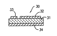
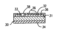
図1は、本発明を適用することができる一般的なパワーMOSFETを示す図である。このパワーMOSFETであるダイ30は、例えば、特許文献3に示されているタイプのダイであるが、シリコンボディ31、上面アルミニウム(すなわち、シリコンを1.0%含むアルミニウム)ソース電極32、アルミニウムゲート電極33、及び容易にはんだ付け可能な従来の三金属電極とすることができる底面ドレイン電極34を含んだ接合部を有する任意の種類のダイとすることができる。上面アルミニウム層は、適当な他の金属材料とすることもできる。接続は通常、ワイヤボンディングによってアルミニウム電極32及び33に対して実施される。
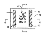
31 シリコンボディ
32 ソース電極
33 ゲート電極
34 ドレイン電極
36,37 コンタクトポスト
38 パッシベーション層
40,41 ソースコンタクト
45 金属クリップ
46 脚(leg)
48 ウェブ(web)
49 開口
60 導電性接着剤
61,62 ギャップ
70 モールドコンパウンド
80 クリップ
81 ウェブ
82,83,84 脚
82,83,84 突起
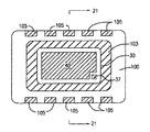
100 カップ形クリップ
101 表面
102,103 エポキシ
105 突起面
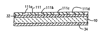
110 ウェーハ
111 ソルダマスク
111a−111d 開口
112a−112d 金属
Claims (24)
- 主要な表面上に設けられる少なくとも1つの電極を有する複数のダイを半導体ウェーハに形成するステップと、
前記半導体ウェーハの前記ダイの少なくとも1つの電極をマスク材料で覆うステップと、
前記各電極に向けて少なくとも1つの開口を前記マスク材料に形成し、前記開口が前記各電極の底面に達するようにするステップと、
前記各電極に向けて前記各開口の底面に少なくとも金属層を形成するステップと、
前記半導体ウェーハから各ダイを個別化するステップと
を有することを特徴とする半導体ダイの製造方法。 - 前記ダイが、パワー半導体デバイスであることを特徴とする請求項1に記載の半導体ダイの製造方法。
- 前記ダイが、パワーMOSFETであることを特徴とする請求項1に記載の半導体ダイの製造方法。
- 前記少なくとも1つの電極が、ソース電極であることを特徴とする請求項3に記載の半導体ダイの製造方法。
- 前記各ダイの前記主要な表面上に第2の電極を備えることを特徴とする請求項1に記載の半導体ダイの製造方法。
- 前記第2の電極が、ゲート電極であることを特徴とする請求項5に記載の半導体ダイの製造方法。
- 前記マスク材料が、フォトイメージ性のソルダマスクであることを特徴とする請求項1に記載の半導体ダイの製造方法。
- 前記マスク材料が、エポキシであることを特徴とする請求項1に記載の半導体ダイの製造方法。
- 前記エポキシが、感光性であることを特徴とする請求項8に記載の半導体ダイの製造方法。
- 前記マスク材料が、メッキレジストとして機能することを特徴とする請求項1に記載の半導体ダイの製造方法。
- 前記マスク材料が、パッシベーションとして機能することを特徴とする請求項1に記載の半導体ダイの製造方法。
- 前記マスク材料が、窒化シリコンからなることを特徴とする請求項1に記載の半導体ダイの製造方法。
- 前記開口するステップが、レチクルで行われることを特徴とする請求項1に記載の半導体ダイの製造方法。
- 前記開口するステップが、レーザエッチングで行われることを特徴とする請求項1に記載の半導体ダイの製造方法。
- 前記少なくとも1つの金属層が、メッキによって形成されることを特徴とする請求項1に記載の半導体ダイの製造方法。
- 前記少なくとも1つの金属層が、ニッケルからなることを特徴とする請求項15に記載の半導体ダイの製造方法。
- 前記1つの金属層の上面に第2の金属層を形成するステップを有することを特徴とする請求項1に記載の半導体ダイの製造方法。
- 前記第2の金属層が、金からなることを特徴とする請求項17に記載の半導体ダイの製造方法。
- 前記第2の金属層が、スズからなることを特徴とする請求項17に記載の半導体ダイの製造方法。
- 前記第2の金属層が、銅からなることを特徴とする請求項17に記載の半導体ダイの製造方法。
- 前記第2の金属層の上面に第3の金属層を形成するステップを有することを特徴とする請求項17に記載の半導体ダイの製造方法。
- 前記第3の金属層が、銀からなることを特徴とする請求項21に記載の半導体ダイの製造方法。
- 前記第2の金属層が、メッキされていることを特徴とする請求項17に記載の半導体ダイの製造方法。
- 前記第3の金属層が、メッキされていることを特徴とする請求項22に記載の半導体ダイの製造方法。
Applications Claiming Priority (2)
| Application Number | Priority Date | Filing Date | Title |
|---|---|---|---|
| US19452200P | 2000-04-04 | 2000-04-04 | |
| US09/819,774 US6624522B2 (en) | 2000-04-04 | 2001-03-28 | Chip scale surface mounted device and process of manufacture |
Related Parent Applications (1)
| Application Number | Title | Priority Date | Filing Date |
|---|---|---|---|
| JP2005226633A Division JP4343158B2 (ja) | 2000-04-04 | 2005-08-04 | 半導体デバイスのパッケージ製造方法 |
Publications (1)
| Publication Number | Publication Date |
|---|---|
| JP2009105437A true JP2009105437A (ja) | 2009-05-14 |
Family
ID=26890112
Family Applications (3)
| Application Number | Title | Priority Date | Filing Date |
|---|---|---|---|
| JP2001573539A Expired - Fee Related JP3768158B2 (ja) | 2000-04-04 | 2001-03-29 | 半導体デバイス |
| JP2005226633A Expired - Fee Related JP4343158B2 (ja) | 2000-04-04 | 2005-08-04 | 半導体デバイスのパッケージ製造方法 |
| JP2009014534A Pending JP2009105437A (ja) | 2000-04-04 | 2009-01-26 | 半導体ダイの製造方法 |
Family Applications Before (2)
| Application Number | Title | Priority Date | Filing Date |
|---|---|---|---|
| JP2001573539A Expired - Fee Related JP3768158B2 (ja) | 2000-04-04 | 2001-03-29 | 半導体デバイス |
| JP2005226633A Expired - Fee Related JP4343158B2 (ja) | 2000-04-04 | 2005-08-04 | 半導体デバイスのパッケージ製造方法 |
Country Status (7)
| Country | Link |
|---|---|
| US (6) | US6624522B2 (ja) |
| EP (1) | EP1287553A4 (ja) |
| JP (3) | JP3768158B2 (ja) |
| CN (1) | CN1316577C (ja) |
| AU (1) | AU2001249587A1 (ja) |
| TW (1) | TW503487B (ja) |
| WO (1) | WO2001075961A1 (ja) |
Families Citing this family (169)
| Publication number | Priority date | Publication date | Assignee | Title |
|---|---|---|---|---|
| US6133634A (en) | 1998-08-05 | 2000-10-17 | Fairchild Semiconductor Corporation | High performance flip chip package |
| US6624522B2 (en) * | 2000-04-04 | 2003-09-23 | International Rectifier Corporation | Chip scale surface mounted device and process of manufacture |
| US6661082B1 (en) * | 2000-07-19 | 2003-12-09 | Fairchild Semiconductor Corporation | Flip chip substrate design |
| US6777786B2 (en) * | 2001-03-12 | 2004-08-17 | Fairchild Semiconductor Corporation | Semiconductor device including stacked dies mounted on a leadframe |
| US6930397B2 (en) * | 2001-03-28 | 2005-08-16 | International Rectifier Corporation | Surface mounted package with die bottom spaced from support board |
| US7119447B2 (en) * | 2001-03-28 | 2006-10-10 | International Rectifier Corporation | Direct fet device for high frequency application |
| US7476964B2 (en) * | 2001-06-18 | 2009-01-13 | International Rectifier Corporation | High voltage semiconductor device housing with increased clearance between housing can and die for improved flux flushing |
| US6784540B2 (en) | 2001-10-10 | 2004-08-31 | International Rectifier Corp. | Semiconductor device package with improved cooling |
| US6891256B2 (en) * | 2001-10-22 | 2005-05-10 | Fairchild Semiconductor Corporation | Thin, thermally enhanced flip chip in a leaded molded package |
| JP3627738B2 (ja) * | 2001-12-27 | 2005-03-09 | 株式会社デンソー | 半導体装置 |
| US6677669B2 (en) * | 2002-01-18 | 2004-01-13 | International Rectifier Corporation | Semiconductor package including two semiconductor die disposed within a common clip |
| US7122884B2 (en) * | 2002-04-16 | 2006-10-17 | Fairchild Semiconductor Corporation | Robust leaded molded packages and methods for forming the same |
| GB0213094D0 (en) * | 2002-06-07 | 2002-07-17 | Power Innovations Ltd | Lead frame |
| US6919599B2 (en) * | 2002-06-28 | 2005-07-19 | International Rectifier Corporation | Short channel trench MOSFET with reduced gate charge |
| JP3942500B2 (ja) * | 2002-07-02 | 2007-07-11 | Necエレクトロニクス株式会社 | 半導体装置の製造方法 |
| JP3853263B2 (ja) | 2002-07-08 | 2006-12-06 | Necエレクトロニクス株式会社 | 半導体装置 |
| US7397137B2 (en) * | 2002-07-15 | 2008-07-08 | International Rectifier Corporation | Direct FET device for high frequency application |
| US7579697B2 (en) * | 2002-07-15 | 2009-08-25 | International Rectifier Corporation | Arrangement for high frequency application |
| US7061077B2 (en) * | 2002-08-30 | 2006-06-13 | Fairchild Semiconductor Corporation | Substrate based unmolded package including lead frame structure and semiconductor die |
| US6777800B2 (en) * | 2002-09-30 | 2004-08-17 | Fairchild Semiconductor Corporation | Semiconductor die package including drain clip |
| US6841865B2 (en) * | 2002-11-22 | 2005-01-11 | International Rectifier Corporation | Semiconductor device having clips for connecting to external elements |
| US7088004B2 (en) * | 2002-11-27 | 2006-08-08 | International Rectifier Corporation | Flip-chip device having conductive connectors |
| US6867481B2 (en) * | 2003-04-11 | 2005-03-15 | Fairchild Semiconductor Corporation | Lead frame structure with aperture or groove for flip chip in a leaded molded package |
| US6946744B2 (en) * | 2003-04-24 | 2005-09-20 | Power-One Limited | System and method of reducing die attach stress and strain |
| JP3759131B2 (ja) | 2003-07-31 | 2006-03-22 | Necエレクトロニクス株式会社 | リードレスパッケージ型半導体装置とその製造方法 |
| CN100454529C (zh) * | 2003-10-24 | 2009-01-21 | 国际整流器公司 | 用于形成互连结构的焊膏以及由焊膏形成的互连结构 |
| US7315081B2 (en) * | 2003-10-24 | 2008-01-01 | International Rectifier Corporation | Semiconductor device package utilizing proud interconnect material |
| JP4312616B2 (ja) | 2004-01-26 | 2009-08-12 | Necエレクトロニクス株式会社 | 半導体装置 |
| US8368211B2 (en) | 2004-03-11 | 2013-02-05 | International Rectifier Corporation | Solderable top metalization and passivation for source mounted package |
| US20050269677A1 (en) * | 2004-05-28 | 2005-12-08 | Martin Standing | Preparation of front contact for surface mounting |
| US7678680B2 (en) * | 2004-06-03 | 2010-03-16 | International Rectifier Corporation | Semiconductor device with reduced contact resistance |
| US8390131B2 (en) | 2004-06-03 | 2013-03-05 | International Rectifier Corporation | Semiconductor device with reduced contact resistance |
| US7235877B2 (en) * | 2004-09-23 | 2007-06-26 | International Rectifier Corporation | Redistributed solder pads using etched lead frame |
| CN100524711C (zh) * | 2004-09-23 | 2009-08-05 | 国际整流器公司 | 使用蚀刻引线框的半导体设备和半导体封装的制造方法 |
| JP4153932B2 (ja) * | 2004-09-24 | 2008-09-24 | 株式会社東芝 | 半導体装置および半導体装置の製造方法 |
| US7692316B2 (en) * | 2004-10-01 | 2010-04-06 | International Rectifier Corporation | Audio amplifier assembly |
| US7394158B2 (en) * | 2004-10-21 | 2008-07-01 | Siliconix Technology C.V. | Solderable top metal for SiC device |
| US7812441B2 (en) * | 2004-10-21 | 2010-10-12 | Siliconix Technology C.V. | Schottky diode with improved surge capability |
| JP2006222298A (ja) | 2005-02-10 | 2006-08-24 | Renesas Technology Corp | 半導体装置およびその製造方法 |
| US7394151B2 (en) * | 2005-02-15 | 2008-07-01 | Alpha & Omega Semiconductor Limited | Semiconductor package with plated connection |
| US7834376B2 (en) | 2005-03-04 | 2010-11-16 | Siliconix Technology C. V. | Power semiconductor switch |
| US9419092B2 (en) | 2005-03-04 | 2016-08-16 | Vishay-Siliconix | Termination for SiC trench devices |
| US7524701B2 (en) * | 2005-04-20 | 2009-04-28 | International Rectifier Corporation | Chip-scale package |
| US7230333B2 (en) | 2005-04-21 | 2007-06-12 | International Rectifier Corporation | Semiconductor package |
| US8466546B2 (en) * | 2005-04-22 | 2013-06-18 | International Rectifier Corporation | Chip-scale package |
| JP4490861B2 (ja) * | 2005-04-25 | 2010-06-30 | 日立協和エンジニアリング株式会社 | 基板 |
| US7682935B2 (en) * | 2005-06-08 | 2010-03-23 | International Rectifier Corporation | Process of manufacture of ultra thin semiconductor wafers with bonded conductive hard carrier |
| US20070013053A1 (en) * | 2005-07-12 | 2007-01-18 | Peter Chou | Semiconductor device and method for manufacturing a semiconductor device |
| US7514769B1 (en) * | 2005-08-13 | 2009-04-07 | National Semiconductor Corporation | Micro surface mount die package and method |
| US7504733B2 (en) | 2005-08-17 | 2009-03-17 | Ciclon Semiconductor Device Corp. | Semiconductor die package |
| US8125083B2 (en) | 2005-09-02 | 2012-02-28 | International Rectifier Corporation | Protective barrier layer for semiconductor device electrodes |
| US7569927B2 (en) * | 2005-09-21 | 2009-08-04 | Microsemi Corporation | RF power transistor package |
| US7560808B2 (en) * | 2005-10-19 | 2009-07-14 | Texas Instruments Incorporated | Chip scale power LDMOS device |
| US8368165B2 (en) | 2005-10-20 | 2013-02-05 | Siliconix Technology C. V. | Silicon carbide Schottky diode |
| US7786558B2 (en) * | 2005-10-20 | 2010-08-31 | Infineon Technologies Ag | Semiconductor component and methods to produce a semiconductor component |
| US7968984B2 (en) | 2005-10-25 | 2011-06-28 | International Rectifier Corporation | Universal pad arrangement for surface mounted semiconductor devices |
| US8089147B2 (en) * | 2005-11-02 | 2012-01-03 | International Rectifier Corporation | IMS formed as can for semiconductor housing |
| JP4591330B2 (ja) * | 2005-11-25 | 2010-12-01 | パナソニック株式会社 | 電子部品接続構造および電子部品接続方法 |
| US20070158796A1 (en) * | 2005-12-09 | 2007-07-12 | International Rectifier Corporation | Semiconductor package |
| DE102005061015B4 (de) * | 2005-12-19 | 2008-03-13 | Infineon Technologies Ag | Verfahren zum Herstellen eines Halbleiterbauteils mit einem vertikalen Halbleiterbauelement |
| US8018056B2 (en) * | 2005-12-21 | 2011-09-13 | International Rectifier Corporation | Package for high power density devices |
| US8698294B2 (en) * | 2006-01-24 | 2014-04-15 | Stats Chippac Ltd. | Integrated circuit package system including wide flange leadframe |
| US7749877B2 (en) * | 2006-03-07 | 2010-07-06 | Siliconix Technology C. V. | Process for forming Schottky rectifier with PtNi silicide Schottky barrier |
| US7446375B2 (en) * | 2006-03-14 | 2008-11-04 | Ciclon Semiconductor Device Corp. | Quasi-vertical LDMOS device having closed cell layout |
| US20070215997A1 (en) * | 2006-03-17 | 2007-09-20 | Martin Standing | Chip-scale package |
| US7663212B2 (en) * | 2006-03-21 | 2010-02-16 | Infineon Technologies Ag | Electronic component having exposed surfaces |
| US20070222087A1 (en) * | 2006-03-27 | 2007-09-27 | Sangdo Lee | Semiconductor device with solderable loop contacts |
| GB2436739B (en) * | 2006-03-31 | 2008-03-12 | Int Rectifier Corp | Process for fabricating a semiconductor package |
| US7554188B2 (en) | 2006-04-13 | 2009-06-30 | International Rectifier Corporation | Low inductance bond-wireless co-package for high power density devices, especially for IGBTs and diodes |
| US7541681B2 (en) * | 2006-05-04 | 2009-06-02 | Infineon Technologies Ag | Interconnection structure, electronic component and method of manufacturing the same |
| US7476978B2 (en) * | 2006-05-17 | 2009-01-13 | Infineon Technologies, Ag | Electronic component having a semiconductor power device |
| US7757392B2 (en) | 2006-05-17 | 2010-07-20 | Infineon Technologies Ag | Method of producing an electronic component |
| US7626262B2 (en) * | 2006-06-14 | 2009-12-01 | Infineon Technologies Ag | Electrically conductive connection, electronic component and method for their production |
| WO2008016619A1 (en) | 2006-07-31 | 2008-02-07 | Vishay-Siliconix | Molybdenum barrier metal for sic schottky diode and process of manufacture |
| US7719096B2 (en) * | 2006-08-11 | 2010-05-18 | Vishay General Semiconductor Llc | Semiconductor device and method for manufacturing a semiconductor device |
| DE102006044690B4 (de) * | 2006-09-22 | 2010-07-29 | Infineon Technologies Ag | Elektronisches Bauteil und Verfahren zum Herstellen |
| DE102006047761A1 (de) * | 2006-10-06 | 2008-04-10 | Infineon Technologies Ag | Halbleiterbauteil und Verfahren zu dessen Herstellung |
| KR100818101B1 (ko) * | 2006-11-08 | 2008-03-31 | 주식회사 하이닉스반도체 | 웨이퍼 레벨 칩 사이즈 패키지 |
| US8552543B2 (en) * | 2006-11-13 | 2013-10-08 | International Rectifier Corporation | Semiconductor package |
| US8106501B2 (en) * | 2008-12-12 | 2012-01-31 | Fairchild Semiconductor Corporation | Semiconductor die package including low stress configuration |
| DE102007007142B4 (de) * | 2007-02-09 | 2008-11-13 | Infineon Technologies Ag | Nutzen, Halbleiterbauteil sowie Verfahren zu deren Herstellung |
| US7880280B2 (en) * | 2007-02-16 | 2011-02-01 | Infineon Technologies Ag | Electronic component and method for manufacturing an electronic component |
| US9147644B2 (en) | 2008-02-26 | 2015-09-29 | International Rectifier Corporation | Semiconductor device and passive component integration in a semiconductor package |
| US8786072B2 (en) * | 2007-02-27 | 2014-07-22 | International Rectifier Corporation | Semiconductor package |
| US8083832B2 (en) * | 2007-02-27 | 2011-12-27 | International Rectifier Corporation | Paste for forming an interconnect and interconnect formed from the paste |
| US7447041B2 (en) * | 2007-03-01 | 2008-11-04 | Delphi Technologies, Inc. | Compression connection for vertical IC packages |
| US8686554B2 (en) * | 2007-03-13 | 2014-04-01 | International Rectifier Corporation | Vertically mountable semiconductor device package |
| JP2008235837A (ja) * | 2007-03-23 | 2008-10-02 | Matsushita Electric Ind Co Ltd | 半導体装置及びその製造方法 |
| GB2448117B (en) | 2007-03-30 | 2009-06-03 | Cambridge Semiconductor Ltd | Forward power converter controllers |
| US7759777B2 (en) * | 2007-04-16 | 2010-07-20 | Infineon Technologies Ag | Semiconductor module |
| US7838985B2 (en) * | 2007-07-12 | 2010-11-23 | Vishay General Semiconductor Llc | Semiconductor assembly that includes a power semiconductor die located on a cell defined by first and second patterned polymer layers |
| US7915728B2 (en) * | 2007-07-12 | 2011-03-29 | Vishay General Semiconductor Llc | Subassembly that includes a power semiconductor die and a heat sink having an exposed surface portion thereof |
| US7879652B2 (en) * | 2007-07-26 | 2011-02-01 | Infineon Technologies Ag | Semiconductor module |
| US20090057855A1 (en) * | 2007-08-30 | 2009-03-05 | Maria Clemens Quinones | Semiconductor die package including stand off structures |
| US8421214B2 (en) * | 2007-10-10 | 2013-04-16 | Vishay General Semiconductor Llc | Semiconductor device and method for manufacturing a semiconductor device |
| US7701065B2 (en) * | 2007-10-26 | 2010-04-20 | Infineon Technologies Ag | Device including a semiconductor chip having a plurality of electrodes |
| US7799614B2 (en) * | 2007-12-21 | 2010-09-21 | Infineon Technologies Ag | Method of fabricating a power electronic device |
| US8426960B2 (en) * | 2007-12-21 | 2013-04-23 | Alpha & Omega Semiconductor, Inc. | Wafer level chip scale packaging |
| JP5153316B2 (ja) * | 2007-12-21 | 2013-02-27 | 新光電気工業株式会社 | 半導体パッケージ用放熱板およびそのめっき方法 |
| JP2009164442A (ja) * | 2008-01-09 | 2009-07-23 | Nec Electronics Corp | 半導体装置 |
| US8143729B2 (en) * | 2008-01-25 | 2012-03-27 | International Rectifier Corporation | Autoclave capable chip-scale package |
| US7955893B2 (en) * | 2008-01-31 | 2011-06-07 | Alpha & Omega Semiconductor, Ltd | Wafer level chip scale package and process of manufacture |
| US7968378B2 (en) * | 2008-02-06 | 2011-06-28 | Infineon Technologies Ag | Electronic device |
| US7972906B2 (en) * | 2008-03-07 | 2011-07-05 | Fairchild Semiconductor Corporation | Semiconductor die package including exposed connections |
| US8637341B2 (en) * | 2008-03-12 | 2014-01-28 | Infineon Technologies Ag | Semiconductor module |
| US7759163B2 (en) * | 2008-04-18 | 2010-07-20 | Infineon Technologies Ag | Semiconductor module |
| US8680658B2 (en) * | 2008-05-30 | 2014-03-25 | Alpha And Omega Semiconductor Incorporated | Conductive clip for semiconductor device package |
| US8053891B2 (en) * | 2008-06-30 | 2011-11-08 | Alpha And Omega Semiconductor Incorporated | Standing chip scale package |
| US7932180B2 (en) | 2008-07-07 | 2011-04-26 | Infineon Technologies Ag | Manufacturing a semiconductor device via etching a semiconductor chip to a first layer |
| US7910992B2 (en) | 2008-07-15 | 2011-03-22 | Maxim Integrated Products, Inc. | Vertical MOSFET with through-body via for gate |
| US8441804B2 (en) * | 2008-07-25 | 2013-05-14 | Infineon Technologies Ag | Semiconductor device and method of manufacturing a semiconductor device |
| US8110912B2 (en) | 2008-07-31 | 2012-02-07 | Infineon Technologies Ag | Semiconductor device |
| US7982292B2 (en) | 2008-08-25 | 2011-07-19 | Infineon Technologies Ag | Semiconductor device |
| US7767495B2 (en) | 2008-08-25 | 2010-08-03 | Infineon Technologies Ag | Method for the fabrication of semiconductor devices including attaching chips to each other with a dielectric material |
| US7923350B2 (en) * | 2008-09-09 | 2011-04-12 | Infineon Technologies Ag | Method of manufacturing a semiconductor device including etching to etch stop regions |
| US8373257B2 (en) * | 2008-09-25 | 2013-02-12 | Alpha & Omega Semiconductor Incorporated | Top exposed clip with window array |
| US8710665B2 (en) | 2008-10-06 | 2014-04-29 | Infineon Technologies Ag | Electronic component, a semiconductor wafer and a method for producing an electronic component |
| US7898067B2 (en) | 2008-10-31 | 2011-03-01 | Fairchild Semiconductor Corporaton | Pre-molded, clip-bonded multi-die semiconductor package |
| US7994646B2 (en) * | 2008-12-17 | 2011-08-09 | Infineon Technologies Ag | Semiconductor device |
| US7851856B2 (en) * | 2008-12-29 | 2010-12-14 | Alpha & Omega Semiconductor, Ltd | True CSP power MOSFET based on bottom-source LDMOS |
| US8049312B2 (en) * | 2009-01-12 | 2011-11-01 | Texas Instruments Incorporated | Semiconductor device package and method of assembly thereof |
| JP5420274B2 (ja) | 2009-03-02 | 2014-02-19 | パナソニック株式会社 | 半導体装置及びその製造方法 |
| US8358014B2 (en) * | 2009-05-28 | 2013-01-22 | Texas Instruments Incorporated | Structure and method for power field effect transistor |
| US8563360B2 (en) * | 2009-06-08 | 2013-10-22 | Alpha And Omega Semiconductor, Inc. | Power semiconductor device package and fabrication method |
| US8222078B2 (en) * | 2009-07-22 | 2012-07-17 | Alpha And Omega Semiconductor Incorporated | Chip scale surface mounted semiconductor device package and process of manufacture |
| JP5500936B2 (ja) * | 2009-10-06 | 2014-05-21 | イビデン株式会社 | 回路基板及び半導体モジュール |
| US7939370B1 (en) * | 2009-10-29 | 2011-05-10 | Alpha And Omega Semiconductor Incorporated | Power semiconductor package |
| JP2011151109A (ja) * | 2010-01-20 | 2011-08-04 | Fuji Electric Co Ltd | 半導体装置およびその製造方法 |
| JP5375708B2 (ja) * | 2010-03-29 | 2013-12-25 | パナソニック株式会社 | 半導体装置の製造方法 |
| US8362606B2 (en) | 2010-07-29 | 2013-01-29 | Alpha & Omega Semiconductor, Inc. | Wafer level chip scale package |
| EP2453476A1 (en) * | 2010-11-12 | 2012-05-16 | Nxp B.V. | Semiconductor device packaging method and semiconductor device package |
| US20120175688A1 (en) | 2011-01-10 | 2012-07-12 | International Rectifier Corporation | Semiconductor Package with Reduced On-Resistance and Top Metal Spreading Resistance with Application to Power Transistor Packaging |
| US8546925B2 (en) | 2011-09-28 | 2013-10-01 | Texas Instruments Incorporated | Synchronous buck converter having coplanar array of contact bumps of equal volume |
| US8906747B2 (en) * | 2012-05-23 | 2014-12-09 | Freescale Semiconductor, Inc. | Cavity-type semiconductor package and method of packaging same |
| US8970035B2 (en) | 2012-08-31 | 2015-03-03 | Taiwan Semiconductor Manufacturing Company, Ltd. | Bump structures for semiconductor package |
| US9202811B2 (en) | 2012-12-18 | 2015-12-01 | Infineon Technologies Americas Corp. | Cascode circuit integration of group III-N and group IV devices |
| US9041067B2 (en) | 2013-02-11 | 2015-05-26 | International Rectifier Corporation | Integrated half-bridge circuit with low side and high side composite switches |
| US8865523B2 (en) * | 2013-03-15 | 2014-10-21 | Alpha & Omega Semiconductor, Inc. | Semiconductor package and fabrication method thereof |
| US9070721B2 (en) | 2013-03-15 | 2015-06-30 | Semiconductor Components Industries, Llc | Semiconductor devices and methods of making the same |
| JP6167397B2 (ja) * | 2013-04-26 | 2017-07-26 | パナソニックIpマネジメント株式会社 | 半導体装置 |
| DE102013212446A1 (de) * | 2013-06-27 | 2015-01-15 | Zf Friedrichshafen Ag | Elektrische Schaltung und Verfahren zum Herstellen einer elektrischen Schaltung zur Ansteuerung einer Last |
| US20150001696A1 (en) * | 2013-06-28 | 2015-01-01 | Infineon Technologies Ag | Semiconductor die carrier structure and method of manufacturing the same |
| US9536800B2 (en) | 2013-12-07 | 2017-01-03 | Fairchild Semiconductor Corporation | Packaged semiconductor devices and methods of manufacturing |
| US9704787B2 (en) * | 2014-10-16 | 2017-07-11 | Infineon Technologies Americas Corp. | Compact single-die power semiconductor package |
| US9570379B2 (en) | 2013-12-09 | 2017-02-14 | Infineon Technologies Americas Corp. | Power semiconductor package with integrated heat spreader and partially etched conductive carrier |
| US9620475B2 (en) | 2013-12-09 | 2017-04-11 | Infineon Technologies Americas Corp | Array based fabrication of power semiconductor package with integrated heat spreader |
| US9653386B2 (en) | 2014-10-16 | 2017-05-16 | Infineon Technologies Americas Corp. | Compact multi-die power semiconductor package |
| US9214419B2 (en) * | 2014-02-28 | 2015-12-15 | Alpha And Omega Semiconductor Incorporated | Power semiconductor device and preparation method thereof |
| JP6287341B2 (ja) * | 2014-03-03 | 2018-03-07 | セイコーエプソン株式会社 | 液体吐出装置および液体吐出装置の制御方法 |
| CN104916597B (zh) * | 2014-03-14 | 2018-06-05 | 尼克森微电子股份有限公司 | 晶圆级扇出芯片的封装方法及封装结构 |
| TWI546906B (zh) | 2014-03-14 | 2016-08-21 | 尼克森微電子股份有限公司 | 晶圓級扇出晶片的封裝結構及封裝方法 |
| JP2015231027A (ja) * | 2014-06-06 | 2015-12-21 | 住友電気工業株式会社 | 半導体装置 |
| CN105448871B (zh) * | 2014-08-18 | 2019-03-08 | 万国半导体股份有限公司 | 功率半导体器件及制备方法 |
| EP3065172B1 (en) | 2015-03-06 | 2024-12-04 | Nexperia B.V. | Semiconductor device |
| DE102015205695B4 (de) * | 2015-03-30 | 2020-09-24 | Robert Bosch Gmbh | Halbleiterbauelement, Kontaktanordnung und Verfahren zur Herstellung |
| DE102015104996B4 (de) * | 2015-03-31 | 2020-06-18 | Infineon Technologies Austria Ag | Halbleitervorrichtungen mit Steuer- und Lastleitungen von entgegengesetzter Richtung |
| CN104900546A (zh) * | 2015-05-04 | 2015-09-09 | 嘉兴斯达半导体股份有限公司 | 一种功率模块的封装结构 |
| CN107710400A (zh) * | 2015-07-01 | 2018-02-16 | 松下知识产权经营株式会社 | 半导体装置 |
| DE102015221971A1 (de) * | 2015-11-09 | 2017-05-11 | Robert Bosch Gmbh | Halbleiterchip mit lötbarer Vorderseite und Verfahren zur Herstellung eines Halbleiterchips |
| US10256168B2 (en) | 2016-06-12 | 2019-04-09 | Nexperia B.V. | Semiconductor device and lead frame therefor |
| CN106711100A (zh) * | 2016-08-22 | 2017-05-24 | 杰群电子科技(东莞)有限公司 | 一种半导体封装结构及加工方法 |
| US10128170B2 (en) | 2017-01-09 | 2018-11-13 | Silanna Asia Pte Ltd | Conductive clip connection arrangements for semiconductor packages |
| JP6894544B2 (ja) * | 2018-07-17 | 2021-06-30 | 富士電機株式会社 | 半導体装置の製造方法 |
| US11355470B2 (en) | 2020-02-27 | 2022-06-07 | Amkor Technology Singapore Holding Pte. Ltd. | Semiconductor device and methods of manufacturing semiconductor devices |
| EP4044226A1 (en) * | 2021-02-16 | 2022-08-17 | Nexperia B.V. | A semiconductor device and a method of manufacturing of a semiconductor device |
| CN114156167A (zh) * | 2021-11-30 | 2022-03-08 | 华虹半导体(无锡)有限公司 | 版图图形 |
| CN115394657B (zh) * | 2022-05-31 | 2024-10-01 | 浙江禾芯集成电路有限公司 | 一种应用于平面型功率器件的封装结构的封装方法 |
| JP7474557B1 (ja) | 2022-12-22 | 2024-04-25 | ヌヴォトンテクノロジージャパン株式会社 | 蓄電パック、半導体装置、および、半導体装置の製造方法 |
| US12464669B2 (en) | 2023-02-24 | 2025-11-04 | Amkor Technology Singapore Holding Pte. Ltd. | Electronic devices and methods of manufacturing electronic devices |
Citations (2)
| Publication number | Priority date | Publication date | Assignee | Title |
|---|---|---|---|---|
| JPH0745620A (ja) * | 1993-07-26 | 1995-02-14 | Hitachi Ltd | 半導体装置およびその製造方法並びにその実装構造体 |
| JPH1022336A (ja) * | 1996-06-28 | 1998-01-23 | Sanyo Electric Co Ltd | 半導体装置の製造方法 |
Family Cites Families (68)
| Publication number | Priority date | Publication date | Assignee | Title |
|---|---|---|---|---|
| US3403438A (en) | 1964-12-02 | 1968-10-01 | Corning Glass Works | Process for joining transistor chip to printed circuit |
| US3871014A (en) | 1969-08-14 | 1975-03-11 | Ibm | Flip chip module with non-uniform solder wettable areas on the substrate |
| US3972062A (en) | 1973-10-04 | 1976-07-27 | Motorola, Inc. | Mounting assemblies for a plurality of transistor integrated circuit chips |
| GB1487945A (en) | 1974-11-20 | 1977-10-05 | Ibm | Semiconductor integrated circuit devices |
| US4454454A (en) | 1983-05-13 | 1984-06-12 | Motorola, Inc. | MOSFET "H" Switch circuit for a DC motor |
| US4646129A (en) | 1983-09-06 | 1987-02-24 | General Electric Company | Hermetic power chip packages |
| US4604644A (en) | 1985-01-28 | 1986-08-05 | International Business Machines Corporation | Solder interconnection structure for joining semiconductor devices to substrates that have improved fatigue life, and process for making |
| US4639760A (en) | 1986-01-21 | 1987-01-27 | Motorola, Inc. | High power RF transistor assembly |
| JPH0676790B2 (ja) * | 1987-07-30 | 1994-09-28 | 株式会社東芝 | イグナイタ |
| JPH07118514B2 (ja) * | 1989-04-24 | 1995-12-18 | 株式会社東芝 | 半田バンプ型半導体装置 |
| US5075759A (en) | 1989-07-21 | 1991-12-24 | Motorola, Inc. | Surface mounting semiconductor device and method |
| US5182632A (en) | 1989-11-22 | 1993-01-26 | Tactical Fabs, Inc. | High density multichip package with interconnect structure and heatsink |
| US5047833A (en) | 1990-10-17 | 1991-09-10 | International Rectifier Corporation | Solderable front metal contact for MOS devices |
| JP2984068B2 (ja) | 1991-01-31 | 1999-11-29 | 株式会社日立製作所 | 半導体装置の製造方法 |
| JPH05129516A (ja) * | 1991-11-01 | 1993-05-25 | Hitachi Ltd | 半導体装置 |
| CA2089435C (en) | 1992-02-14 | 1997-12-09 | Kenzi Kobayashi | Semiconductor device |
| JP2833326B2 (ja) | 1992-03-03 | 1998-12-09 | 松下電器産業株式会社 | 電子部品実装接続体およびその製造方法 |
| JPH065401A (ja) | 1992-06-23 | 1994-01-14 | Mitsubishi Electric Corp | チップ型抵抗素子及び半導体装置 |
| JPH0637143A (ja) | 1992-07-15 | 1994-02-10 | Toshiba Corp | 半導体装置および半導体装置の製造方法 |
| US5394490A (en) | 1992-08-11 | 1995-02-28 | Hitachi, Ltd. | Semiconductor device having an optical waveguide interposed in the space between electrode members |
| US5313366A (en) | 1992-08-12 | 1994-05-17 | International Business Machines Corporation | Direct chip attach module (DCAM) |
| JPH06244231A (ja) | 1993-02-01 | 1994-09-02 | Motorola Inc | 気密半導体デバイスおよびその製造方法 |
| US5371404A (en) | 1993-02-04 | 1994-12-06 | Motorola, Inc. | Thermally conductive integrated circuit package with radio frequency shielding |
| JP2795788B2 (ja) | 1993-02-18 | 1998-09-10 | シャープ株式会社 | 半導体チップの実装方法 |
| US5703405A (en) | 1993-03-15 | 1997-12-30 | Motorola, Inc. | Integrated circuit chip formed from processing two opposing surfaces of a wafer |
| US5510758A (en) | 1993-04-07 | 1996-04-23 | Matsushita Electric Industrial Co., Ltd. | Multilayer microstrip wiring board with a semiconductor device mounted thereon via bumps |
| JP3258764B2 (ja) | 1993-06-01 | 2002-02-18 | 三菱電機株式会社 | 樹脂封止型半導体装置の製造方法ならびに外部引出用電極およびその製造方法 |
| US5397921A (en) | 1993-09-03 | 1995-03-14 | Advanced Semiconductor Assembly Technology | Tab grid array |
| US5455456A (en) | 1993-09-15 | 1995-10-03 | Lsi Logic Corporation | Integrated circuit package lid |
| US5451544A (en) | 1993-10-15 | 1995-09-19 | International Rectifier Corporation | Method of manufacturing a back contact for semiconductor die |
| US5734201A (en) | 1993-11-09 | 1998-03-31 | Motorola, Inc. | Low profile semiconductor device with like-sized chip and mounting substrate |
| US5367435A (en) | 1993-11-16 | 1994-11-22 | International Business Machines Corporation | Electronic package structure and method of making same |
| US5454160A (en) | 1993-12-03 | 1995-10-03 | Ncr Corporation | Apparatus and method for stacking integrated circuit devices |
| JPH07193184A (ja) | 1993-12-27 | 1995-07-28 | Fujitsu Ltd | マルチチップモジュールの製造方法及びマルチチップモジュール |
| JP3073644B2 (ja) | 1993-12-28 | 2000-08-07 | 株式会社東芝 | 半導体装置 |
| US5446316A (en) * | 1994-01-06 | 1995-08-29 | Harris Corporation | Hermetic package for a high power semiconductor device |
| US5578869A (en) * | 1994-03-29 | 1996-11-26 | Olin Corporation | Components for housing an integrated circuit device |
| US6486003B1 (en) * | 1996-12-13 | 2002-11-26 | Tessera, Inc. | Expandable interposer for a microelectronic package and method therefor |
| JP3377867B2 (ja) | 1994-08-12 | 2003-02-17 | 京セラ株式会社 | 半導体素子収納用パッケージ |
| JP2546192B2 (ja) | 1994-09-30 | 1996-10-23 | 日本電気株式会社 | フィルムキャリア半導体装置 |
| US5532512A (en) | 1994-10-03 | 1996-07-02 | General Electric Company | Direct stacked and flip chip power semiconductor device structures |
| JP3138159B2 (ja) | 1994-11-22 | 2001-02-26 | シャープ株式会社 | 半導体装置、半導体装置実装体、及び半導体装置の交換方法 |
| US5904499A (en) | 1994-12-22 | 1999-05-18 | Pace; Benedict G | Package for power semiconductor chips |
| JPH08335653A (ja) | 1995-04-07 | 1996-12-17 | Nitto Denko Corp | 半導体装置およびその製法並びに上記半導体装置の製造に用いる半導体装置用テープキャリア |
| US5655703A (en) | 1995-05-25 | 1997-08-12 | International Business Machines Corporation | Solder hierarchy for chip attachment to substrates |
| US5674785A (en) | 1995-11-27 | 1997-10-07 | Micron Technology, Inc. | Method of producing a single piece package for semiconductor die |
| US5726502A (en) | 1996-04-26 | 1998-03-10 | Motorola, Inc. | Bumped semiconductor device with alignment features and method for making the same |
| CN1179626A (zh) * | 1996-09-05 | 1998-04-22 | 国际整流器公司 | 一种改进的表面封装的大功率半导体封壳及其制造方法 |
| US5814884C1 (en) * | 1996-10-24 | 2002-01-29 | Int Rectifier Corp | Commonly housed diverse semiconductor die |
| KR100209760B1 (ko) * | 1996-12-19 | 1999-07-15 | 구본준 | 반도체 패키지 및 이의 제조방법 |
| US6051888A (en) | 1997-04-07 | 2000-04-18 | Texas Instruments Incorporated | Semiconductor package and method for increased thermal dissipation of flip-chip semiconductor package |
| KR100219806B1 (ko) * | 1997-05-27 | 1999-09-01 | 윤종용 | 반도체장치의 플립 칩 실장형 솔더 범프의 제조방법, 이에 따라 제조되는 솔더범프 및 그 분석방법 |
| JPH1154673A (ja) | 1997-07-31 | 1999-02-26 | Nec Kansai Ltd | 半導体装置 |
| GB9725960D0 (en) | 1997-12-08 | 1998-02-04 | Westinghouse Brake & Signal | Encapsulating semiconductor chips |
| JP3654485B2 (ja) * | 1997-12-26 | 2005-06-02 | 富士通株式会社 | 半導体装置の製造方法 |
| JP3097644B2 (ja) * | 1998-01-06 | 2000-10-10 | 日本電気株式会社 | 半導体装置接続構造及び接続方法 |
| US6423623B1 (en) * | 1998-06-09 | 2002-07-23 | Fairchild Semiconductor Corporation | Low Resistance package for semiconductor devices |
| EP0966038A3 (en) * | 1998-06-15 | 2001-02-28 | Ford Motor Company | Bonding of semiconductor power devices |
| EP0978871A3 (en) * | 1998-08-05 | 2001-12-19 | Harris Corporation | A low power packaging design |
| US6133634A (en) | 1998-08-05 | 2000-10-17 | Fairchild Semiconductor Corporation | High performance flip chip package |
| US6268275B1 (en) * | 1998-10-08 | 2001-07-31 | Micron Technology, Inc. | Method of locating conductive spheres utilizing screen and hopper of solder balls |
| KR20000057810A (ko) * | 1999-01-28 | 2000-09-25 | 가나이 쓰토무 | 반도체 장치 |
| JP4408475B2 (ja) * | 1999-02-23 | 2010-02-03 | 三洋電機株式会社 | ボンディングワイヤを採用しない半導体装置 |
| US6744124B1 (en) * | 1999-12-10 | 2004-06-01 | Siliconix Incorporated | Semiconductor die package including cup-shaped leadframe |
| US6624522B2 (en) | 2000-04-04 | 2003-09-23 | International Rectifier Corporation | Chip scale surface mounted device and process of manufacture |
| US6362087B1 (en) * | 2000-05-05 | 2002-03-26 | Aptos Corporation | Method for fabricating a microelectronic fabrication having formed therein a redistribution structure |
| JP3467454B2 (ja) | 2000-06-05 | 2003-11-17 | Necエレクトロニクス株式会社 | 半導体装置の製造方法 |
| US6391687B1 (en) | 2000-10-31 | 2002-05-21 | Fairchild Semiconductor Corporation | Column ball grid array package |
-
2001
- 2001-03-28 US US09/819,774 patent/US6624522B2/en not_active Expired - Lifetime
- 2001-03-29 WO PCT/US2001/010074 patent/WO2001075961A1/en not_active Ceased
- 2001-03-29 EP EP01922828A patent/EP1287553A4/en not_active Withdrawn
- 2001-03-29 JP JP2001573539A patent/JP3768158B2/ja not_active Expired - Fee Related
- 2001-03-29 AU AU2001249587A patent/AU2001249587A1/en not_active Abandoned
- 2001-03-29 CN CNB018100015A patent/CN1316577C/zh not_active Expired - Fee Related
- 2001-04-03 TW TW090107971A patent/TW503487B/zh not_active IP Right Cessation
-
2003
- 2003-08-05 US US10/634,453 patent/US6767820B2/en not_active Expired - Lifetime
- 2003-08-05 US US10/634,447 patent/US7122887B2/en not_active Expired - Lifetime
-
2004
- 2004-06-07 US US10/863,530 patent/US6890845B2/en not_active Expired - Lifetime
-
2005
- 2005-04-27 US US11/116,157 patent/US7253090B2/en not_active Expired - Lifetime
- 2005-08-04 JP JP2005226633A patent/JP4343158B2/ja not_active Expired - Fee Related
-
2006
- 2006-06-05 US US11/446,878 patent/US7476979B2/en not_active Expired - Lifetime
-
2009
- 2009-01-26 JP JP2009014534A patent/JP2009105437A/ja active Pending
Patent Citations (2)
| Publication number | Priority date | Publication date | Assignee | Title |
|---|---|---|---|---|
| JPH0745620A (ja) * | 1993-07-26 | 1995-02-14 | Hitachi Ltd | 半導体装置およびその製造方法並びにその実装構造体 |
| JPH1022336A (ja) * | 1996-06-28 | 1998-01-23 | Sanyo Electric Co Ltd | 半導体装置の製造方法 |
Also Published As
| Publication number | Publication date |
|---|---|
| JP3768158B2 (ja) | 2006-04-19 |
| JP4343158B2 (ja) | 2009-10-14 |
| US20040026796A1 (en) | 2004-02-12 |
| US7476979B2 (en) | 2009-01-13 |
| US20010048116A1 (en) | 2001-12-06 |
| TW503487B (en) | 2002-09-21 |
| EP1287553A1 (en) | 2003-03-05 |
| US20060220123A1 (en) | 2006-10-05 |
| CN1316577C (zh) | 2007-05-16 |
| JP2005354105A (ja) | 2005-12-22 |
| JP2004500720A (ja) | 2004-01-08 |
| US7253090B2 (en) | 2007-08-07 |
| EP1287553A4 (en) | 2007-11-07 |
| WO2001075961A1 (en) | 2001-10-11 |
| WO2001075961A8 (en) | 2002-02-07 |
| US20040224438A1 (en) | 2004-11-11 |
| US7122887B2 (en) | 2006-10-17 |
| AU2001249587A1 (en) | 2001-10-15 |
| US20050186707A1 (en) | 2005-08-25 |
| HK1057648A1 (en) | 2004-04-08 |
| US6890845B2 (en) | 2005-05-10 |
| CN1430791A (zh) | 2003-07-16 |
| US6624522B2 (en) | 2003-09-23 |
| US6767820B2 (en) | 2004-07-27 |
| US20040038509A1 (en) | 2004-02-26 |
Similar Documents
| Publication | Publication Date | Title |
|---|---|---|
| JP4343158B2 (ja) | 半導体デバイスのパッケージ製造方法 | |
| JP4195380B2 (ja) | 冷却を改善した半導体デバイスのパッケージ | |
| US5596231A (en) | High power dissipation plastic encapsulated package for integrated circuit die | |
| JP2005506691A5 (ja) | ||
| KR101561684B1 (ko) | 반도체 다이 패키지 및 그의 제조 방법 | |
| US6451627B1 (en) | Semiconductor device and process for manufacturing and packaging a semiconductor device | |
| TWI399836B (zh) | 晶圓級晶片尺寸封裝及製造方法 | |
| US11004775B2 (en) | SMDS integration on QFN by 3D stacked solution | |
| US7390698B2 (en) | Packaged semiconductor device and method of manufacture using shaped die | |
| JP5103731B2 (ja) | モールドパッケージ | |
| CN100524711C (zh) | 使用蚀刻引线框的半导体设备和半导体封装的制造方法 | |
| HK1057648B (en) | Chip scale surface mounted device and process of manufacture | |
| JP2883065B2 (ja) | 半導体装置 | |
| JPH0311641A (ja) | 半導体装置 |
Legal Events
| Date | Code | Title | Description |
|---|---|---|---|
| A621 | Written request for application examination |
Free format text: JAPANESE INTERMEDIATE CODE: A621 Effective date: 20090126 |
|
| RD02 | Notification of acceptance of power of attorney |
Free format text: JAPANESE INTERMEDIATE CODE: A7422 Effective date: 20100416 |
|
| RD04 | Notification of resignation of power of attorney |
Free format text: JAPANESE INTERMEDIATE CODE: A7424 Effective date: 20100428 |
|
| A131 | Notification of reasons for refusal |
Free format text: JAPANESE INTERMEDIATE CODE: A131 Effective date: 20120306 |
|
| A977 | Report on retrieval |
Free format text: JAPANESE INTERMEDIATE CODE: A971007 Effective date: 20120308 |
|
| A02 | Decision of refusal |
Free format text: JAPANESE INTERMEDIATE CODE: A02 Effective date: 20120731 |