JP2009141002A - 絶縁層を有する酸化物半導体素子およびそれを用いた表示装置 - Google Patents
絶縁層を有する酸化物半導体素子およびそれを用いた表示装置 Download PDFInfo
- Publication number
- JP2009141002A JP2009141002A JP2007313579A JP2007313579A JP2009141002A JP 2009141002 A JP2009141002 A JP 2009141002A JP 2007313579 A JP2007313579 A JP 2007313579A JP 2007313579 A JP2007313579 A JP 2007313579A JP 2009141002 A JP2009141002 A JP 2009141002A
- Authority
- JP
- Japan
- Prior art keywords
- insulating layer
- oxide semiconductor
- layer
- electrode
- gate
- Prior art date
- Legal status (The legal status is an assumption and is not a legal conclusion. Google has not performed a legal analysis and makes no representation as to the accuracy of the status listed.)
- Granted
Links
Images


Classifications
-
- H—ELECTRICITY
- H10—SEMICONDUCTOR DEVICES; ELECTRIC SOLID-STATE DEVICES NOT OTHERWISE PROVIDED FOR
- H10D—INORGANIC ELECTRIC SEMICONDUCTOR DEVICES
- H10D30/00—Field-effect transistors [FET]
- H10D30/60—Insulated-gate field-effect transistors [IGFET]
- H10D30/67—Thin-film transistors [TFT]
- H10D30/674—Thin-film transistors [TFT] characterised by the active materials
- H10D30/6755—Oxide semiconductors, e.g. zinc oxide, copper aluminium oxide or cadmium stannate
-
- H—ELECTRICITY
- H10—SEMICONDUCTOR DEVICES; ELECTRIC SOLID-STATE DEVICES NOT OTHERWISE PROVIDED FOR
- H10D—INORGANIC ELECTRIC SEMICONDUCTOR DEVICES
- H10D30/00—Field-effect transistors [FET]
- H10D30/60—Insulated-gate field-effect transistors [IGFET]
- H10D30/67—Thin-film transistors [TFT]
- H10D30/6704—Thin-film transistors [TFT] having supplementary regions or layers in the thin films or in the insulated bulk substrates for controlling properties of the device
-
- H—ELECTRICITY
- H10—SEMICONDUCTOR DEVICES; ELECTRIC SOLID-STATE DEVICES NOT OTHERWISE PROVIDED FOR
- H10D—INORGANIC ELECTRIC SEMICONDUCTOR DEVICES
- H10D30/00—Field-effect transistors [FET]
- H10D30/60—Insulated-gate field-effect transistors [IGFET]
- H10D30/67—Thin-film transistors [TFT]
- H10D30/6729—Thin-film transistors [TFT] characterised by the electrodes
- H10D30/6737—Thin-film transistors [TFT] characterised by the electrodes characterised by the electrode materials
- H10D30/6739—Conductor-insulator-semiconductor electrodes
Landscapes
- Thin Film Transistor (AREA)
- Liquid Crystal (AREA)
- Electroluminescent Light Sources (AREA)
- Dram (AREA)
- Devices For Indicating Variable Information By Combining Individual Elements (AREA)
Abstract
【解決手段】 酸化物半導体層に接する絶縁層を有する酸化物半導体素子であって、前記絶縁層が、酸化物半導体に接する膜厚50nm以上のSiとOとを含む酸化物からなる第1の絶縁層と、該第1の絶縁層に接する膜厚50nm以上のSiとNとを含む窒化物からなる第2の絶縁層と、該第2の絶縁層に接する第3の絶縁層と、を有する。
【選択図】 図1
Description
(PECVD:Plasma Enhanced Chemical Vapor Deposition)
図1(a)、(b)における酸化物半導体素子を作成する基板10としては、以下の低温プロセス用で使用可能な基板を用いることができる。具体的には、ポリエチレン・テレフタレート(PET)、ポリエチレン・ナフタレート(PEN)、ポリイミド、ポリカーボネートなど250℃以下のプロセスで有効とされるプラスチックのフィルム、並びに薄板を用いることが可能である。ただし、これらの低温プロセス用の基板は、一般にガス透過性もしくはガス放出性が高く、バリア層10aを形成し酸化物半導体層15への影響を抑制する必要がある。また、低アルカリガラス基板に対しても、半導体素子形成プロセス中のアルカリ金属元素の図1(a)におけるゲート絶縁層12もしくは図1(b)におけるゲート絶縁層12a、bへの拡散防止のためのバリア層10aを用いる必要がある。さらには酸化物半導体層15への拡散の防止のためのバリア層10aを用いる必要がある。
図1(a)、(b)における酸化物半導体層15は、Sn、In、Znの少なくとも1種類の元素を含み構成されるアモルファス酸化物を用いることが可能である。
本発明の絶縁層には酸化物半導体の還元を抑制する機能が要求される。この還元抑制機能には、当該絶縁層自身によって酸化物半導体を還元させない機能と、バリア層から拡散する水素原子を酸化物半導体層に拡散することを抑制する機能という2つの異なる機能が必要である。
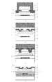
上記アモルファス酸化物半導体、並びに絶縁層を用いて、図9に示すボトムゲート・ボトムコンタクト型薄膜トランジスタを作成することができる。
図12(a)に本発明の絶縁層を保護層に用いたボトムゲート・トップコンタクト型薄膜トランジスタを示す。ゲート電極11、ゲート絶縁層12、酸化物半導体層15、ソース電極13およびドレイン電極14、保護層として機能する第1〜第3の絶縁層16〜18を上述の図9の説明と同様に形成し、図12(a)の構造を得る。この際、第1の絶縁層16、あるいは、第1と第2の絶縁層16、17をソース電極13およびドレイン電極14を形成する前に堆積し、フォトリゾグラフィー法等を使用してそれら絶縁層をパターニングして、図12(b)または(c)の構成をとっても良い。図12(a)〜(c)の何れ構成においても酸化物半導体層上に3層の絶縁層が形成される。
図13(a)に本発明の絶縁層を保護層に用いたトッブゲート・ボトムコンタクト型薄膜トランジスタを示す。ソース電極13およびドレイン電極14、酸化物半導体層15、ゲート電極11、ゲート絶縁層や保護層として機能する絶縁層16〜18を前述の図9の説明と同様に形成する。この場合、酸化物半導体の還元抑制に対する機能を持つ第1の絶縁層16がゲート絶縁層12としての機能を兼ねている。また、第2の絶縁層17が第3の絶縁層18からの水素拡散を防止する機能を有している。さらに、図13(b)のように酸化物半導体の還元抑制に対する機能を持つ第1の絶縁層16と水素拡散抑制の機能を持つ第2の絶縁層17をそれぞれ第1のゲート絶縁層12a、第2のゲート絶縁層12bとし、この積層膜をゲート絶縁層12として用いても良い。図13(a)と(b)のいずれの構成においても、酸化物半導体上に3層の絶縁層が形成される。
次に本発明の絶縁層を下地層と保護層の両方に用いた酸化物半導体電界効果トランジスタについて説明する。
これより、本発明の酸化物電界効果トランジスタを用いた表示装置について説明する。
図16に本発明の絶縁層を保護層に用いたボトムゲート・コプレーナ型薄膜トランジスタを示す。
図9のボトムゲート・ボトムコンタクト型の電界効果トランジスタの作製例を示す。まず、ガラス基板10(コーニング社製1737)上に、ゲート電極を形成するための電極層をスパッタ法により形成する。電極材料にはMoを用い、膜厚は50nmである。
図12(d)のボトムゲート・トップコンタクト型の電界効果型トランジスタの作製例を示す。
本実施例は、実施例2のバリアコート層10aをPECVD法により基板温度250℃でSiOmNnで形成する例である。SiOmNn形成時の基板温度は250℃とし、プロセスガスには、SiH4、N2O、N2を用いる。ガス流量比はSiH4:N2O:N2=1:2.5:10に設定する。また、投入RFパワー密度と圧力はそれぞれ0.25W/cm2、150Paとする。N2ガスの代わりにNH3ガスを用いても良い。バリアコート層10a以降は実施例2と同様に形成する。こうして、本発明の電界効果トランジスタを完成させる。
図12(c)のボトムゲート・トップコンタクト型の電界効果型トランジスタの作製例を示す。
図13(b)のトップゲート・コンタクト型の電界効果トランジスタの作製例を示す。
図13(c)のトップゲート・ボトムコンタクト型の電界効果トランジスタの作製例を示す。
図1(b)のバリアコート層上ボトムゲート・ボトムコンタクト型の電界効果トランジスタの作製例を示す。
本実施例ではボトムゲート・ボトムコンタクト型の電界効果トランジスタを用いた図14の表示装置について説明する。電界効果トランジスタの製造工程は、前記実施例1と同様である。ただし、図1(a)、(b)、図9、図12(a)〜(d)、図13(a)〜(c)に記載されるどの電界効果トランジスタを用いても良い。そして、電界効果トランジスタ120のドレイン電極124に保護層127を介して電極130を形成する。電極130にはスパッタ法により形成したITOを用いる。次に電極130上に正孔輸送層131a、発光層131bを蒸着法により形成する。正孔輸送層131a、発光層131bにはそれぞれα‐NPD、Alq3を用いる。さらに発光層131b上に電極132を蒸着法により形成する。電極材料にはMgAgを用いる。このようにして、図14に示す、有機エレクトロルミネッセンス素子を表示素子とする表示装置を作成する。
本実施例ではボトムゲート・ボトムコンタクト型の電界効果トランジスタを用いた図15の表示装置について説明する。電界効果トランジスタの製造工程は、前記実施例1と同様である。ただし、図1(a)、(b)、図9、図12(a)〜(d)、図13(a)〜(c)に記載されるどの電界効果トランジスタを用いても良い。前記電界効果トランジスタ120において、ドレイン電極124をなすITO膜の島の短辺を100μmまで延長する。そして、延長された90μmの部分を残し、ソース電極123およびゲート電極121への配線を確保した上で、電界効果トランジスタ120を絶縁層125〜7で被覆する。この上にポリイミド膜133を塗布し、ラビング工程を施す。
実施例9において、電界効果トランジスタを形成する基板として白色のプラスチック基板110を用い、電界効果トランジスタ120の各電極を金に置き換え、ポリイミド膜133、135と偏光板100、140を廃する構成とする。そして、白色のプラスチック基板110と透明のプラスチック基板150の空隙に粒子と流体を絶縁性皮膜にて被覆したカプセル134を充填させる構成とする。この構成の表示装置の場合、本電界効果トランジスタによって延長されたドレイン電極と上部のITO膜間の電圧が制御され、よってカプセル内の粒子が上下に移動する。それによって、透明基板側から見た延長されたドレイン電極領域の反射率を制御することで表示を行うことができる。
図16のボトムゲート・コプレーナ型の電界効果型トランジスタの作製例を示す。
10a バリアコート層として機能する第3の絶縁層
10b 第2の絶縁層
11 ゲート電極
12 ゲート絶縁層、もしくは、ゲート絶縁層として機能する第1の絶縁層
12a ゲート絶縁層として機能する第2の絶縁層
12b ゲート絶縁層として機能する第1の絶縁層
13 ソース電極
14 ドレイン電極
15 酸化物半導体層
16 保護層として機能する第1の絶縁層
17 保護層として機能する第2の絶縁層
18 保護層として機能する第3の絶縁層
19 ソース配線
20 ドレイン配線
100 偏光板
110 基板
120 電界効果トランジスタ
121 ゲート電極
122 アモルファス酸化物半導体層
123 ソース電極
124 ドレイン電極
125 保護層として機能する第1の絶縁層
126 保護層として機能する第2の絶縁層
127 保護層として機能する第3の絶縁層
130 電極
131a ホール輸送層
131b 発光層
132 電極
133 高抵抗層、あるいは、ポリイミド膜
134 ネマチック液晶、あるいは、電気泳動型粒子セル
135 高抵抗層、あるいは、ポリイミド膜
140 基板
150 偏光板
Claims (10)
- 酸化物半導体層に接する絶縁層を有する酸化物半導体素子であって、
前記絶縁層が、酸化物半導体に接する膜厚50nm以上のSiとOとを含む酸化物からなる第1の絶縁層と、
該第1の絶縁層に接する膜厚50nm以上のSiとNとを含む窒化物からなる第2の絶縁層と、
該第2の絶縁層に接する第3の絶縁層と、
を有することを特徴とする酸化物半導体素子。 - 前記第1の絶縁層及び第2の絶縁層の水素含有量が4×10²¹個/cm3以下であり、第3の絶縁層の水素含有量が4×1021個/cm3より多いことを特徴とする、請求項1に記載の酸化物半導体素子。
- 前記第1の絶縁層がSiOxであり、前記第2の絶縁層がSiNyであり、前記第3の絶縁層がSiNz又はSiOmNnであることを特徴とする請求項1に記載の酸化物半導体素子。
- 前記第1の絶縁層と前記第2の絶縁層とが連続的に形成された絶縁層であることを特徴とする請求項1に記載の酸化物半導体素子。
- 前記酸化物半導体がSn、In、Znの少なくとも1種類の元素を含むアモルファス酸化物半導体であることを特徴とする請求項1に記載の酸化物半導体素子。
- 請求項1から5のいずれか1項に記載の酸化物半導体素子であって、前記第1から第3の絶縁層の少なくとも一部がゲート絶縁層として用いられることを特徴とする酸化物半導体素子。
- 基板上で表示素子の電極と電界効果トランジスタのソース電極またはドレイン電極とが接続されてなる表示装置であって、
該電界効果トランジスタは、請求項1から5のいずれか1項に記載の酸化物半導体素子であることを特徴とする表示装置。 - 前記表示素子は、エレクトロルミネッセンス素子であることを特徴とする請求項7に記載の表示装置。
- 前記表示素子は、液晶セルであることを特徴とする請求項7に記載の表示装置。
- 前記基板上に前記表示素子および前記電界効果トランジスタが二次元状に複数配されていることを特徴とする請求項7から9のいずれか1項に記載の表示装置。
Priority Applications (8)
| Application Number | Priority Date | Filing Date | Title |
|---|---|---|---|
| JP2007313579A JP5213422B2 (ja) | 2007-12-04 | 2007-12-04 | 絶縁層を有する酸化物半導体素子およびそれを用いた表示装置 |
| DE602008005773T DE602008005773D1 (de) | 2007-12-04 | 2008-11-27 | Oxidhalbleitervorrichtung mit isolierungsschicht und anzeigevorrichtung unter benutzung derselben |
| CN2008801187802A CN101884109B (zh) | 2007-12-04 | 2008-11-27 | 包含绝缘层的氧化物半导体器件和使用该器件的显示装置 |
| EP08857495A EP2195849B1 (en) | 2007-12-04 | 2008-11-27 | Oxide semiconductor device including insulating layer and display apparatus using the same |
| US12/679,901 US8502217B2 (en) | 2007-12-04 | 2008-11-27 | Oxide semiconductor device including insulating layer and display apparatus using the same |
| AT08857495T ATE503273T1 (de) | 2007-12-04 | 2008-11-27 | Oxidhalbleitervorrichtung mit isolierungsschicht und anzeigevorrichtung unter benutzung derselben |
| PCT/JP2008/071989 WO2009072532A1 (en) | 2007-12-04 | 2008-11-27 | Oxide semiconductor device including insulating layer and display apparatus using the same |
| TW097146793A TWI422034B (zh) | 2007-12-04 | 2008-12-02 | 包含絕緣層之氧化物半導體裝置及使用氧化物半導體裝置之顯示設備 |
Applications Claiming Priority (1)
| Application Number | Priority Date | Filing Date | Title |
|---|---|---|---|
| JP2007313579A JP5213422B2 (ja) | 2007-12-04 | 2007-12-04 | 絶縁層を有する酸化物半導体素子およびそれを用いた表示装置 |
Publications (2)
| Publication Number | Publication Date |
|---|---|
| JP2009141002A true JP2009141002A (ja) | 2009-06-25 |
| JP5213422B2 JP5213422B2 (ja) | 2013-06-19 |
Family
ID=40467267
Family Applications (1)
| Application Number | Title | Priority Date | Filing Date |
|---|---|---|---|
| JP2007313579A Active JP5213422B2 (ja) | 2007-12-04 | 2007-12-04 | 絶縁層を有する酸化物半導体素子およびそれを用いた表示装置 |
Country Status (8)
| Country | Link |
|---|---|
| US (1) | US8502217B2 (ja) |
| EP (1) | EP2195849B1 (ja) |
| JP (1) | JP5213422B2 (ja) |
| CN (1) | CN101884109B (ja) |
| AT (1) | ATE503273T1 (ja) |
| DE (1) | DE602008005773D1 (ja) |
| TW (1) | TWI422034B (ja) |
| WO (1) | WO2009072532A1 (ja) |
Cited By (135)
| Publication number | Priority date | Publication date | Assignee | Title |
|---|---|---|---|---|
| WO2011013522A1 (en) * | 2009-07-31 | 2011-02-03 | Semiconductor Energy Laboratory Co., Ltd. | Semiconductor device and manufacturing method thereof |
| WO2011013561A1 (en) * | 2009-07-31 | 2011-02-03 | Semiconductor Energy Laboratory Co., Ltd. | Semiconductor device and method for manufacturing the same |
| JP2011049549A (ja) * | 2009-07-31 | 2011-03-10 | Semiconductor Energy Lab Co Ltd | 半導体装置及び半導体装置の作製方法 |
| WO2011037010A1 (en) * | 2009-09-24 | 2011-03-31 | Semiconductor Energy Laboratory Co., Ltd. | Semiconductor element and method for manufacturing the same |
| JP2011077514A (ja) * | 2009-09-04 | 2011-04-14 | Semiconductor Energy Lab Co Ltd | 半導体装置の作製方法 |
| JP2011077517A (ja) * | 2009-09-04 | 2011-04-14 | Semiconductor Energy Lab Co Ltd | 液晶表示装置およびその作製方法 |
| WO2011046015A1 (en) * | 2009-10-16 | 2011-04-21 | Semiconductor Energy Laboratory Co., Ltd. | Logic circuit and semiconductor device |
| WO2011048959A1 (en) * | 2009-10-21 | 2011-04-28 | Semiconductor Energy Laboratory Co., Ltd. | Semiconductor device and method for manufacturing the same |
| JP2011091110A (ja) * | 2009-10-20 | 2011-05-06 | Canon Inc | 酸化物半導体素子を用いた回路及びその製造方法、並びに表示装置 |
| JP2011100991A (ja) * | 2009-10-09 | 2011-05-19 | Semiconductor Energy Lab Co Ltd | 半導体装置およびその作製方法 |
| JP2011100980A (ja) * | 2009-10-05 | 2011-05-19 | Semiconductor Energy Lab Co Ltd | 半導体装置及び半導体装置の作製方法 |
| JP2011109080A (ja) * | 2009-10-21 | 2011-06-02 | Semiconductor Energy Lab Co Ltd | 半導体装置及びその作製方法 |
| JP2011119706A (ja) * | 2009-10-30 | 2011-06-16 | Semiconductor Energy Lab Co Ltd | 半導体装置及び半導体装置の作製方法 |
| JP2011123986A (ja) * | 2009-11-13 | 2011-06-23 | Semiconductor Energy Lab Co Ltd | 半導体装置および半導体装置の駆動方法 |
| JP2011129895A (ja) * | 2009-11-20 | 2011-06-30 | Semiconductor Energy Lab Co Ltd | 半導体装置の作製方法 |
| JP2011170346A (ja) * | 2010-01-24 | 2011-09-01 | Semiconductor Energy Lab Co Ltd | 表示装置 |
| WO2011118515A1 (ja) * | 2010-03-26 | 2011-09-29 | シャープ株式会社 | 表示装置および表示装置用アレイ基板の製造方法 |
| JP2011222736A (ja) * | 2010-04-09 | 2011-11-04 | Semiconductor Energy Lab Co Ltd | 半導体装置および半導体装置の作製方法 |
| JP2011222989A (ja) * | 2010-03-26 | 2011-11-04 | Semiconductor Energy Lab Co Ltd | 半導体装置の作製方法 |
| WO2011145484A1 (en) * | 2010-05-21 | 2011-11-24 | Semiconductor Energy Laboratory Co., Ltd. | Semiconductor device |
| JP2012064929A (ja) * | 2010-08-16 | 2012-03-29 | Semiconductor Energy Lab Co Ltd | 半導体装置の作製方法 |
| WO2012057020A1 (ja) * | 2010-10-28 | 2012-05-03 | 富士フイルム株式会社 | 薄膜トランジスタおよびその製造方法 |
| WO2012063614A1 (ja) * | 2010-11-10 | 2012-05-18 | 株式会社日立製作所 | 半導体装置 |
| KR20120051720A (ko) * | 2009-07-31 | 2012-05-22 | 가부시키가이샤 한도오따이 에네루기 켄큐쇼 | 반도체 장치 및 그 제조 방법 |
| JP2012114421A (ja) * | 2010-11-05 | 2012-06-14 | Semiconductor Energy Lab Co Ltd | 半導体装置及び半導体装置の作製方法 |
| JP2012134520A (ja) * | 2009-07-17 | 2012-07-12 | Semiconductor Energy Lab Co Ltd | 半導体装置 |
| JP2012151460A (ja) * | 2010-12-28 | 2012-08-09 | Semiconductor Energy Lab Co Ltd | 半導体装置、及び半導体装置の作製方法 |
| KR20120090783A (ko) * | 2011-01-12 | 2012-08-17 | 가부시키가이샤 한도오따이 에네루기 켄큐쇼 | 반도체 장치 및 반도체 장치의 제작 방법 |
| JP2012216794A (ja) * | 2011-03-25 | 2012-11-08 | Semiconductor Energy Lab Co Ltd | 酸化物半導体膜の形成方法および半導体装置の作製方法 |
| US8319226B2 (en) | 2008-11-17 | 2012-11-27 | Sony Corporation | Thin film transistor and display device |
| CN102906881A (zh) * | 2010-05-21 | 2013-01-30 | 株式会社半导体能源研究所 | 半导体装置 |
| JP2013033998A (ja) * | 2009-09-04 | 2013-02-14 | Semiconductor Energy Lab Co Ltd | 発光装置 |
| JP2013038396A (ja) * | 2011-07-08 | 2013-02-21 | Semiconductor Energy Lab Co Ltd | 半導体装置およびその作製方法 |
| KR20130038936A (ko) | 2010-07-27 | 2013-04-18 | 가부시키가이샤 한도오따이 에네루기 켄큐쇼 | 반도체 장치 및 그 제작 방법 |
| JP2013077858A (ja) * | 2009-11-13 | 2013-04-25 | Semiconductor Energy Lab Co Ltd | 半導体装置 |
| JP2013102145A (ja) * | 2011-10-14 | 2013-05-23 | Semiconductor Energy Lab Co Ltd | 半導体装置 |
| JP2013138028A (ja) * | 2009-11-04 | 2013-07-11 | Samsung Display Co Ltd | 有機電界発光表示装置の製造方法 |
| JP2013168632A (ja) * | 2012-02-15 | 2013-08-29 | Lg Display Co Ltd | 薄膜トランジスタ、薄膜トランジスタアレイ基板及びそれらの製造方法 |
| JP2013175713A (ja) * | 2012-01-25 | 2013-09-05 | Semiconductor Energy Lab Co Ltd | 半導体装置及び半導体装置の作製方法 |
| WO2013179837A1 (ja) * | 2012-05-28 | 2013-12-05 | シャープ株式会社 | 半導体装置およびその製造方法 |
| JP2013254950A (ja) * | 2012-05-10 | 2013-12-19 | Semiconductor Energy Lab Co Ltd | 半導体装置 |
| WO2014003086A1 (en) * | 2012-06-29 | 2014-01-03 | Semiconductor Energy Laboratory Co., Ltd. | Semiconductor device |
| JP2014007381A (ja) * | 2012-04-13 | 2014-01-16 | Semiconductor Energy Lab Co Ltd | 半導体装置及びその作製方法 |
| US8642380B2 (en) | 2010-07-02 | 2014-02-04 | Semiconductor Energy Laboratory Co., Ltd. | Manufacturing method of semiconductor device |
| JP2014030002A (ja) * | 2012-06-29 | 2014-02-13 | Semiconductor Energy Lab Co Ltd | 半導体装置 |
| JP2014030000A (ja) * | 2012-06-29 | 2014-02-13 | Semiconductor Energy Lab Co Ltd | 半導体装置および半導体装置の作製方法 |
| JP2014033181A (ja) * | 2012-04-06 | 2014-02-20 | Semiconductor Energy Lab Co Ltd | 絶縁膜、及び半導体装置の作製方法、並びに半導体装置 |
| JP2014045094A (ja) * | 2012-08-27 | 2014-03-13 | Sharp Corp | 高透過率保護膜作製方法および半導体発光素子の製造方法 |
| JP2014082515A (ja) * | 2009-10-16 | 2014-05-08 | Semiconductor Energy Lab Co Ltd | 半導体装置 |
| WO2014080826A1 (ja) * | 2012-11-21 | 2014-05-30 | シャープ株式会社 | 表示装置 |
| JP2014103379A (ja) * | 2012-11-20 | 2014-06-05 | Samsung Display Co Ltd | 表示装置 |
| JP2014143404A (ja) * | 2012-12-25 | 2014-08-07 | Semiconductor Energy Lab Co Ltd | 抵抗素子、表示装置、及び電子機器 |
| JP2014183238A (ja) * | 2013-03-19 | 2014-09-29 | Toshiba Corp | 表示装置、薄膜トランジスタ、表示装置の製造方法及び薄膜トランジスタの製造方法 |
| US8872171B2 (en) | 2009-05-29 | 2014-10-28 | Semiconductor Energy Laboratory Co., Ltd. | Semiconductor device and method for manufacturing the same |
| KR101456354B1 (ko) * | 2011-11-03 | 2014-11-03 | 보에 테크놀로지 그룹 컴퍼니 리미티드 | 박막 트랜지스터 어레이 기판 |
| US8890139B2 (en) | 2011-10-19 | 2014-11-18 | Samsung Display Co., Ltd. | Solution composition for passivation layer, thin film transistor array panel, and manufacturing method for thin film transistor array panel |
| US8912027B2 (en) | 2012-07-24 | 2014-12-16 | Samsung Display Co., Ltd | Display device and method of manufacturing the same |
| WO2014208520A1 (ja) * | 2013-06-28 | 2014-12-31 | 株式会社神戸製鋼所 | 薄膜トランジスタおよびその製造方法 |
| JP2015505168A (ja) * | 2012-01-13 | 2015-02-16 | 京東方科技集團股▲ふん▼有限公司 | Tftアレイ基板の製造方法 |
| JP2015035608A (ja) * | 2008-12-19 | 2015-02-19 | 株式会社半導体エネルギー研究所 | 半導体装置及びその作製方法 |
| JP2015043431A (ja) * | 2010-05-20 | 2015-03-05 | 株式会社半導体エネルギー研究所 | 半導体装置 |
| JP2015060996A (ja) * | 2013-09-19 | 2015-03-30 | 株式会社東芝 | 表示装置及び半導体装置 |
| JP2015079969A (ja) * | 2009-08-07 | 2015-04-23 | 株式会社半導体エネルギー研究所 | 発光装置 |
| JP2015090957A (ja) * | 2013-11-07 | 2015-05-11 | Nltテクノロジー株式会社 | イメージセンサ及びその製造方法 |
| US9035301B2 (en) | 2013-06-19 | 2015-05-19 | Semiconductor Energy Laboratory Co., Ltd. | Imaging device |
| JP2015097272A (ja) * | 2009-12-04 | 2015-05-21 | 株式会社半導体エネルギー研究所 | 半導体装置 |
| JP2015515120A (ja) * | 2012-02-28 | 2015-05-21 | 京東方科技集團股▲ふん▼有限公司 | アレイ基板の製造方法及びアレイ基板、ディスプレー |
| KR20150058425A (ko) * | 2012-09-24 | 2015-05-28 | 가부시키가이샤 한도오따이 에네루기 켄큐쇼 | 반도체 장치 |
| JP2015515744A (ja) * | 2012-03-09 | 2015-05-28 | エア プロダクツ アンド ケミカルズ インコーポレイテッドAir Products And Chemicals Incorporated | ディスプレイ・デバイスのためのバリア材料 |
| JP2015109476A (ja) * | 2009-08-07 | 2015-06-11 | 株式会社半導体エネルギー研究所 | 半導体装置 |
| JP2015122344A (ja) * | 2013-12-20 | 2015-07-02 | 株式会社ジャパンディスプレイ | 薄膜トランジスタ及びそれを用いた表示装置 |
| JP2015144288A (ja) * | 2009-11-13 | 2015-08-06 | 株式会社半導体エネルギー研究所 | 半導体装置、及び、半導体装置の作製方法 |
| JP2015156499A (ja) * | 2009-10-09 | 2015-08-27 | 株式会社半導体エネルギー研究所 | 半導体装置 |
| JP2015228505A (ja) * | 2009-10-09 | 2015-12-17 | 株式会社半導体エネルギー研究所 | 半導体装置の作製方法 |
| JP2016021579A (ja) * | 2010-05-21 | 2016-02-04 | 株式会社半導体エネルギー研究所 | 半導体装置 |
| JP2016042584A (ja) * | 2010-05-21 | 2016-03-31 | 株式会社半導体エネルギー研究所 | 半導体装置の作製方法 |
| JP2016048798A (ja) * | 2009-12-08 | 2016-04-07 | 株式会社半導体エネルギー研究所 | 半導体装置 |
| KR20160039542A (ko) * | 2014-10-01 | 2016-04-11 | 도쿄엘렉트론가부시키가이샤 | 전자 디바이스, 그 제조 방법, 및 그 제조 장치 |
| WO2016067585A1 (ja) * | 2014-10-29 | 2016-05-06 | 株式会社Joled | 薄膜半導体装置、有機el表示装置及び薄膜半導体装置の製造方法 |
| JP2016100521A (ja) * | 2014-11-25 | 2016-05-30 | 株式会社ジャパンディスプレイ | 薄膜トランジスタ及びその製造方法 |
| KR20160069063A (ko) * | 2014-12-05 | 2016-06-16 | 삼성디스플레이 주식회사 | 박막 트랜지스터 기판 및 그 제조 방법 |
| JP2016122843A (ja) * | 2009-08-07 | 2016-07-07 | 株式会社半導体エネルギー研究所 | 表示装置 |
| JP2016136276A (ja) * | 2010-04-28 | 2016-07-28 | 株式会社半導体エネルギー研究所 | 表示装置及び電子機器 |
| EP2513893A4 (en) * | 2009-12-18 | 2016-09-07 | Semiconductor Energy Lab | Liquid crystal display device and electronic device |
| US9496404B2 (en) | 2010-03-05 | 2016-11-15 | Semiconductor Energy Laboratory Co., Ltd. | Semiconductor device and manufacturing method thereof |
| JP2016225635A (ja) * | 2010-03-19 | 2016-12-28 | 株式会社半導体エネルギー研究所 | 半導体装置 |
| US9576982B2 (en) | 2011-11-11 | 2017-02-21 | Semiconductor Energy Laboratory Co., Ltd. | Liquid crystal display device, EL display device, and manufacturing method thereof |
| KR20170037647A (ko) * | 2014-09-02 | 2017-04-04 | 가부시키가이샤 고베 세이코쇼 | 박막 트랜지스터 |
| JP2017069589A (ja) * | 2009-10-21 | 2017-04-06 | 株式会社半導体エネルギー研究所 | 半導体装置及び半導体装置の作製方法 |
| JP2017076131A (ja) * | 2011-02-14 | 2017-04-20 | 株式会社半導体エネルギー研究所 | 表示装置 |
| JP2017085128A (ja) * | 2010-02-26 | 2017-05-18 | 株式会社半導体エネルギー研究所 | 半導体装置の作製方法 |
| JP2017098586A (ja) * | 2009-09-04 | 2017-06-01 | 株式会社半導体エネルギー研究所 | 半導体装置 |
| KR20170061721A (ko) * | 2011-06-30 | 2017-06-05 | 어플라이드 머티어리얼스, 인코포레이티드 | PECVD SiO2 패시베이션을 사용한 IGZO 및 ZNO TFT 제조 방법 |
| JP2017103467A (ja) * | 2010-01-24 | 2017-06-08 | 株式会社半導体エネルギー研究所 | 半導体装置 |
| JP2017103481A (ja) * | 2012-03-09 | 2017-06-08 | エア プロダクツ アンド ケミカルズ インコーポレイテッドAir Products And Chemicals Incorporated | 薄膜トランジスター機器上にケイ素含有膜を製造する方法 |
| JP2017108162A (ja) * | 2010-05-21 | 2017-06-15 | 株式会社半導体エネルギー研究所 | 半導体装置の作製方法 |
| JP2017143277A (ja) * | 2010-02-26 | 2017-08-17 | 株式会社半導体エネルギー研究所 | トランジスタ及び液晶表示装置 |
| JP2017156757A (ja) * | 2009-10-09 | 2017-09-07 | 株式会社半導体エネルギー研究所 | 半導体装置及びその作製方法 |
| JP2017175022A (ja) * | 2016-03-24 | 2017-09-28 | 株式会社Joled | 薄膜トランジスタ |
| US9831101B2 (en) | 2009-06-30 | 2017-11-28 | Semiconductor Energy Laboratory Co., Ltd. | Method for manufacturing semiconductor device |
| JP2018018102A (ja) * | 2010-02-26 | 2018-02-01 | 株式会社半導体エネルギー研究所 | 液晶表示装置 |
| KR101823852B1 (ko) * | 2009-09-16 | 2018-03-14 | 가부시키가이샤 한도오따이 에네루기 켄큐쇼 | 트랜지스터 및 표시 장치 |
| US9927896B2 (en) | 2014-10-10 | 2018-03-27 | Samsung Display Co., Ltd. | Display device and method of manufacturing the same |
| JP2018093240A (ja) * | 2009-11-20 | 2018-06-14 | 株式会社半導体エネルギー研究所 | 半導体装置の作製方法 |
| JP2018125536A (ja) * | 2009-09-04 | 2018-08-09 | 株式会社半導体エネルギー研究所 | 表示装置 |
| JP2018189987A (ja) * | 2010-02-11 | 2018-11-29 | 株式会社半導体エネルギー研究所 | 液晶表示装置 |
| JP2018190993A (ja) * | 2013-01-21 | 2018-11-29 | 株式会社半導体エネルギー研究所 | 半導体装置の作製方法 |
| KR20190006092A (ko) * | 2010-06-11 | 2019-01-16 | 가부시키가이샤 한도오따이 에네루기 켄큐쇼 | 반도체 장치 및 그 제조 방법 |
| KR20190015429A (ko) * | 2011-01-26 | 2019-02-13 | 가부시키가이샤 한도오따이 에네루기 켄큐쇼 | 반도체 장치 및 그의 제작 방법 |
| KR20190025741A (ko) * | 2009-12-11 | 2019-03-11 | 가부시키가이샤 한도오따이 에네루기 켄큐쇼 | 반도체 장치 및 그 제작방법 |
| WO2019049632A1 (ja) * | 2017-09-05 | 2019-03-14 | 株式会社アルバック | 半導体装置の製造方法、および、半導体装置 |
| JP2019056908A (ja) * | 2009-10-09 | 2019-04-11 | 株式会社半導体エネルギー研究所 | 表示装置の作製方法 |
| US10332743B2 (en) | 2009-06-30 | 2019-06-25 | Semiconductor Energy Laboratory Co., Ltd. | Method for manufacturing semiconductor device |
| JP2019125809A (ja) * | 2012-05-10 | 2019-07-25 | 株式会社半導体エネルギー研究所 | 半導体装置 |
| JP2019195095A (ja) * | 2009-06-30 | 2019-11-07 | 株式会社半導体エネルギー研究所 | 半導体装置 |
| JP2019212927A (ja) * | 2009-09-24 | 2019-12-12 | 株式会社半導体エネルギー研究所 | 半導体装置 |
| JP2019220705A (ja) * | 2009-12-08 | 2019-12-26 | 株式会社半導体エネルギー研究所 | 半導体装置の作製方法 |
| JP2020030419A (ja) * | 2012-08-23 | 2020-02-27 | 株式会社半導体エネルギー研究所 | 表示装置 |
| JP2020102622A (ja) * | 2018-12-21 | 2020-07-02 | 株式会社半導体エネルギー研究所 | 半導体装置、および半導体装置の作製方法 |
| KR20200083639A (ko) * | 2010-01-20 | 2020-07-08 | 가부시키가이샤 한도오따이 에네루기 켄큐쇼 | 표시 장치 |
| JP2020194969A (ja) * | 2011-09-29 | 2020-12-03 | 株式会社半導体エネルギー研究所 | 半導体装置 |
| JP2021106294A (ja) * | 2009-12-04 | 2021-07-26 | 株式会社半導体エネルギー研究所 | 半導体装置 |
| JP2022069560A (ja) * | 2011-03-11 | 2022-05-11 | 株式会社半導体エネルギー研究所 | 半導体装置 |
| JP2022123009A (ja) * | 2013-02-28 | 2022-08-23 | 株式会社半導体エネルギー研究所 | 半導体装置 |
| JP2022141674A (ja) * | 2010-05-21 | 2022-09-29 | 株式会社半導体エネルギー研究所 | 液晶表示装置 |
| KR20220135226A (ko) * | 2009-09-04 | 2022-10-06 | 가부시키가이샤 한도오따이 에네루기 켄큐쇼 | 표시장치 및 전자기기 |
| JP2022169521A (ja) * | 2009-11-27 | 2022-11-09 | 株式会社半導体エネルギー研究所 | 半導体装置 |
| US11502110B2 (en) | 2020-03-18 | 2022-11-15 | Samsung Display Co., Ltd. | Display device and method of manufacturing the same |
| JP2023036811A (ja) * | 2010-07-26 | 2023-03-14 | 株式会社半導体エネルギー研究所 | 半導体装置 |
| JP2024026618A (ja) * | 2010-04-02 | 2024-02-28 | 株式会社半導体エネルギー研究所 | 半導体装置 |
| JP2024050718A (ja) * | 2009-12-11 | 2024-04-10 | 株式会社半導体エネルギー研究所 | 半導体装置 |
| JP2025013365A (ja) * | 2009-09-24 | 2025-01-24 | 株式会社半導体エネルギー研究所 | 半導体装置 |
| JP2025041657A (ja) * | 2009-12-04 | 2025-03-26 | 株式会社半導体エネルギー研究所 | 半導体装置 |
| JP2025083367A (ja) * | 2009-11-28 | 2025-05-30 | 株式会社半導体エネルギー研究所 | 半導体装置 |
| US12614531B1 (en) | 2010-01-20 | 2026-04-28 | Semiconductor Energy Laboratory Co., Ltd. | Display device |
Families Citing this family (77)
| Publication number | Priority date | Publication date | Assignee | Title |
|---|---|---|---|---|
| TWI495108B (zh) * | 2008-07-31 | 2015-08-01 | 半導體能源研究所股份有限公司 | 半導體裝置的製造方法 |
| JP5627071B2 (ja) | 2008-09-01 | 2014-11-19 | 株式会社半導体エネルギー研究所 | 半導体装置の作製方法 |
| CN103972246B (zh) * | 2009-07-27 | 2017-05-31 | 株式会社神户制钢所 | 布线结构以及具备布线结构的显示装置 |
| WO2011013502A1 (en) | 2009-07-31 | 2011-02-03 | Semiconductor Energy Laboratory Co., Ltd. | Semiconductor device and manufacturing method thereof |
| WO2011027676A1 (en) | 2009-09-04 | 2011-03-10 | Semiconductor Energy Laboratory Co., Ltd. | Semiconductor device and manufacturing method thereof |
| WO2011027701A1 (en) * | 2009-09-04 | 2011-03-10 | Semiconductor Energy Laboratory Co., Ltd. | Light-emitting device and method for manufacturing the same |
| CN105185837B (zh) * | 2009-10-08 | 2018-08-03 | 株式会社半导体能源研究所 | 半导体器件、显示装置和电子电器 |
| WO2011043218A1 (en) | 2009-10-09 | 2011-04-14 | Semiconductor Energy Laboratory Co., Ltd. | Semiconductor device and method for manufacturing the same |
| CN102598280B (zh) | 2009-10-21 | 2016-05-18 | 株式会社半导体能源研究所 | 液晶显示器件及包括该液晶显示器件的电子设备 |
| KR20260036405A (ko) | 2009-10-29 | 2026-03-16 | 가부시키가이샤 한도오따이 에네루기 켄큐쇼 | 반도체 장치 |
| WO2011052385A1 (en) | 2009-10-30 | 2011-05-05 | Semiconductor Energy Laboratory Co., Ltd. | Semiconductor device |
| KR20170072965A (ko) | 2009-11-13 | 2017-06-27 | 가부시키가이샤 한도오따이 에네루기 켄큐쇼 | 스퍼터링 타겟 및 그 제조방법, 및 트랜지스터 |
| KR101623961B1 (ko) * | 2009-12-02 | 2016-05-26 | 삼성전자주식회사 | 트랜지스터와 그 제조방법 및 트랜지스터를 포함하는 전자소자 |
| KR101729933B1 (ko) * | 2009-12-18 | 2017-04-25 | 가부시키가이샤 한도오따이 에네루기 켄큐쇼 | 불휘발성 래치 회로와 논리 회로, 및 이를 사용한 반도체 장치 |
| KR102480794B1 (ko) | 2009-12-28 | 2022-12-22 | 가부시키가이샤 한도오따이 에네루기 켄큐쇼 | 기억 장치와 반도체 장치 |
| US8879010B2 (en) | 2010-01-24 | 2014-11-04 | Semiconductor Energy Laboratory Co., Ltd. | Display device |
| CN102754209B (zh) | 2010-02-12 | 2015-11-25 | 株式会社半导体能源研究所 | 半导体装置及其驱动方法 |
| US8617920B2 (en) * | 2010-02-12 | 2013-12-31 | Semiconductor Energy Laboratory Co., Ltd. | Semiconductor device and manufacturing method thereof |
| KR20130008037A (ko) * | 2010-03-05 | 2013-01-21 | 가부시키가이샤 한도오따이 에네루기 켄큐쇼 | 반도체 장치를 제작하는 방법 |
| WO2011118509A1 (en) | 2010-03-26 | 2011-09-29 | Semiconductor Energy Laboratory Co., Ltd. | Method for manufacturing semiconductor device |
| GB2479150B (en) | 2010-03-30 | 2013-05-15 | Pragmatic Printing Ltd | Transistor and its method of manufacture |
| KR101465192B1 (ko) | 2010-04-09 | 2014-11-25 | 가부시키가이샤 한도오따이 에네루기 켄큐쇼 | 반도체 장치 |
| WO2011132529A1 (en) * | 2010-04-23 | 2011-10-27 | Semiconductor Energy Laboratory Co., Ltd. | Method for manufacturing semiconductor device |
| WO2011132625A1 (en) | 2010-04-23 | 2011-10-27 | Semiconductor Energy Laboratory Co., Ltd. | Manufacturing method of semiconductor device |
| WO2011132548A1 (en) | 2010-04-23 | 2011-10-27 | Semiconductor Energy Laboratory Co., Ltd. | Semiconductor device and manufacturing method thereof |
| US9496405B2 (en) | 2010-05-20 | 2016-11-15 | Semiconductor Energy Laboratory Co., Ltd. | Method for manufacturing semiconductor device including step of adding cation to oxide semiconductor layer |
| US8552425B2 (en) * | 2010-06-18 | 2013-10-08 | Semiconductor Energy Laboratory Co., Ltd. | Semiconductor device |
| WO2012002186A1 (en) | 2010-07-02 | 2012-01-05 | Semiconductor Energy Laboratory Co., Ltd. | Semiconductor device |
| JP2012033836A (ja) * | 2010-08-03 | 2012-02-16 | Canon Inc | トップゲート型薄膜トランジスタ及びこれを備えた表示装置 |
| US8422272B2 (en) | 2010-08-06 | 2013-04-16 | Semiconductor Energy Laboratory Co., Ltd. | Semiconductor device and driving method thereof |
| US8786815B2 (en) | 2010-09-07 | 2014-07-22 | Au Optronics Corporation | Driving circuit and display panel having the same |
| KR20200052993A (ko) * | 2010-12-03 | 2020-05-15 | 가부시키가이샤 한도오따이 에네루기 켄큐쇼 | 산화물 반도체막 및 반도체 장치 |
| KR20120063809A (ko) * | 2010-12-08 | 2012-06-18 | 삼성전자주식회사 | 박막 트랜지스터 표시판 |
| US8894825B2 (en) | 2010-12-17 | 2014-11-25 | Semiconductor Energy Laboratory Co., Ltd. | Sputtering target, method for manufacturing the same, manufacturing semiconductor device |
| US9012904B2 (en) * | 2011-03-25 | 2015-04-21 | Semiconductor Energy Laboratory Co., Ltd. | Semiconductor device and method for manufacturing the same |
| TWI545652B (zh) | 2011-03-25 | 2016-08-11 | 半導體能源研究所股份有限公司 | 半導體裝置及其製造方法 |
| US9006803B2 (en) * | 2011-04-22 | 2015-04-14 | Semiconductor Energy Laboratory Co., Ltd. | Semiconductor device and method for manufacturing thereof |
| US9166055B2 (en) | 2011-06-17 | 2015-10-20 | Semiconductor Energy Laboratory Co., Ltd. | Semiconductor device and method for manufacturing the same |
| US9214474B2 (en) | 2011-07-08 | 2015-12-15 | Semiconductor Energy Laboratory Co., Ltd. | Semiconductor device and method for manufacturing semiconductor device |
| US8952377B2 (en) | 2011-07-08 | 2015-02-10 | Semiconductor Energy Laboratory Co., Ltd. | Semiconductor device and manufacturing method thereof |
| US9660092B2 (en) | 2011-08-31 | 2017-05-23 | Semiconductor Energy Laboratory Co., Ltd. | Oxide semiconductor thin film transistor including oxygen release layer |
| KR20130043063A (ko) | 2011-10-19 | 2013-04-29 | 가부시키가이샤 한도오따이 에네루기 켄큐쇼 | 반도체 장치 및 반도체 장치의 제작 방법 |
| TWI567985B (zh) | 2011-10-21 | 2017-01-21 | 半導體能源研究所股份有限公司 | 半導體裝置及其製造方法 |
| JP6122275B2 (ja) | 2011-11-11 | 2017-04-26 | 株式会社半導体エネルギー研究所 | 表示装置 |
| KR101942980B1 (ko) * | 2012-01-17 | 2019-01-29 | 삼성디스플레이 주식회사 | 반도체 디바이스 및 그 형성 방법 |
| CN102683422B (zh) * | 2012-03-21 | 2016-03-23 | 京东方科技集团股份有限公司 | 氧化物薄膜晶体管及制作方法、阵列基板、显示装置 |
| KR102932705B1 (ko) | 2012-04-13 | 2026-02-27 | 가부시키가이샤 한도오따이 에네루기 켄큐쇼 | 반도체 장치 |
| CN102683424B (zh) | 2012-04-28 | 2013-08-07 | 京东方科技集团股份有限公司 | 显示装置、阵列基板、薄膜晶体管及其制作方法 |
| US8860023B2 (en) | 2012-05-01 | 2014-10-14 | Semiconductor Energy Laboratory Co., Ltd. | Semiconductor device |
| CN102709189A (zh) * | 2012-05-21 | 2012-10-03 | 京东方科技集团股份有限公司 | 一种薄膜晶体管及其制作方法及一种阵列基板 |
| US8957694B2 (en) * | 2012-05-22 | 2015-02-17 | Broadcom Corporation | Wafer level package resistance monitor scheme |
| WO2014046222A1 (en) | 2012-09-24 | 2014-03-27 | Semiconductor Energy Laboratory Co., Ltd. | Display device |
| WO2014061762A1 (en) | 2012-10-17 | 2014-04-24 | Semiconductor Energy Laboratory Co., Ltd. | Semiconductor device and method for manufacturing the same |
| CN103000628B (zh) * | 2012-12-14 | 2015-04-22 | 京东方科技集团股份有限公司 | 显示装置、阵列基板及其制作方法 |
| JP6152729B2 (ja) * | 2013-03-26 | 2017-06-28 | ソニー株式会社 | 撮像装置および撮像表示システム |
| JP6151070B2 (ja) * | 2013-04-11 | 2017-06-21 | 株式会社ジャパンディスプレイ | 薄膜トランジスタ及びそれを用いた表示装置 |
| US10304859B2 (en) | 2013-04-12 | 2019-05-28 | Semiconductor Energy Laboratory Co., Ltd. | Semiconductor device having an oxide film on an oxide semiconductor film |
| CN103236441B (zh) * | 2013-04-22 | 2015-11-25 | 深圳市华星光电技术有限公司 | 开关管及其制备方法、显示面板 |
| TWI635750B (zh) | 2013-08-02 | 2018-09-11 | 半導體能源研究所股份有限公司 | 攝像裝置以及其工作方法 |
| CN103456745B (zh) * | 2013-09-10 | 2016-09-07 | 北京京东方光电科技有限公司 | 一种阵列基板及其制备方法、显示装置 |
| JP2016001712A (ja) | 2013-11-29 | 2016-01-07 | 株式会社半導体エネルギー研究所 | 半導体装置の作製方法 |
| KR102296917B1 (ko) * | 2014-09-15 | 2021-09-02 | 삼성디스플레이 주식회사 | 플렉서블 디스플레이 장치 및 그 제조방법 |
| KR102337370B1 (ko) | 2014-10-22 | 2021-12-09 | 삼성디스플레이 주식회사 | 반도체 소자 및 반도체 소자의 제조 방법 |
| TWI629791B (zh) * | 2015-04-13 | 2018-07-11 | 友達光電股份有限公司 | 主動元件結構及其製作方法 |
| TWI613706B (zh) * | 2015-07-03 | 2018-02-01 | Au Optronics Corp. | 氧化物半導體薄膜電晶體及其製作方法 |
| JP6685675B2 (ja) * | 2015-09-07 | 2020-04-22 | 株式会社Joled | 有機el素子、それを用いた有機el表示パネル、及び有機el表示パネルの製造方法 |
| CN106449732B (zh) * | 2015-10-29 | 2020-04-21 | 陆磊 | 一种薄膜晶体管及制造方法和显示器面板 |
| US9773787B2 (en) | 2015-11-03 | 2017-09-26 | Semiconductor Energy Laboratory Co., Ltd. | Semiconductor device, memory device, electronic device, or method for driving the semiconductor device |
| US9853210B2 (en) * | 2015-11-17 | 2017-12-26 | International Business Machines Corporation | Reduced process degradation of spin torque magnetoresistive random access memory |
| WO2017153882A1 (en) * | 2016-03-11 | 2017-09-14 | Semiconductor Energy Laboratory Co., Ltd. | Semiconductor device, manufacturing method thereof, and display device including the semiconductor device |
| CN108780756B (zh) | 2016-03-18 | 2021-10-22 | 株式会社理光 | 用于制造场效应晶体管的方法 |
| TWI778959B (zh) * | 2017-03-03 | 2022-10-01 | 日商半導體能源硏究所股份有限公司 | 半導體裝置及半導體裝置的製造方法 |
| CN107516647B (zh) * | 2017-08-18 | 2021-02-26 | 京东方科技集团股份有限公司 | 阵列基板及其制作方法、显示装置 |
| US11121263B2 (en) | 2019-08-27 | 2021-09-14 | Apple Inc. | Hydrogen trap layer for display device and the same |
| JP2021044426A (ja) * | 2019-09-12 | 2021-03-18 | キオクシア株式会社 | 半導体記憶装置 |
| JP2024000908A (ja) * | 2022-06-21 | 2024-01-09 | キオクシア株式会社 | 半導体装置及び半導体記憶装置 |
| CN115835682A (zh) * | 2022-11-25 | 2023-03-21 | 合肥京东方卓印科技有限公司 | 封装材料、封装膜层、显示面板和显示装置 |
Citations (5)
| Publication number | Priority date | Publication date | Assignee | Title |
|---|---|---|---|---|
| JP2003086808A (ja) * | 2001-09-10 | 2003-03-20 | Masashi Kawasaki | 薄膜トランジスタおよびマトリクス表示装置 |
| JP2007073562A (ja) * | 2005-09-02 | 2007-03-22 | Kochi Prefecture Sangyo Shinko Center | 薄膜トランジスタ |
| JP2007123861A (ja) * | 2005-09-29 | 2007-05-17 | Semiconductor Energy Lab Co Ltd | 半導体装置及びその作製方法 |
| JP2007220817A (ja) * | 2006-02-15 | 2007-08-30 | Kochi Prefecture Sangyo Shinko Center | 薄膜トランジスタ及びその製法 |
| JP2008141119A (ja) * | 2006-12-05 | 2008-06-19 | Canon Inc | 酸化物半導体を用いた表示装置及びその製造方法 |
Family Cites Families (22)
| Publication number | Priority date | Publication date | Assignee | Title |
|---|---|---|---|---|
| JPS63101740A (ja) | 1986-10-17 | 1988-05-06 | Nippon Telegr & Teleph Corp <Ntt> | 縦型電界効果トランジスタ型ガスセンサ |
| JP3445187B2 (ja) | 1999-08-03 | 2003-09-08 | キヤノン株式会社 | 半導体素子の欠陥補償方法 |
| JP4089858B2 (ja) | 2000-09-01 | 2008-05-28 | 国立大学法人東北大学 | 半導体デバイス |
| JP2002206168A (ja) | 2000-10-24 | 2002-07-26 | Canon Inc | シリコン系薄膜の形成方法、シリコン系半導体層の形成方法及び光起電力素子 |
| US6858308B2 (en) | 2001-03-12 | 2005-02-22 | Canon Kabushiki Kaisha | Semiconductor element, and method of forming silicon-based film |
| JP2003007629A (ja) | 2001-04-03 | 2003-01-10 | Canon Inc | シリコン系膜の形成方法、シリコン系膜および半導体素子 |
| JP2004289034A (ja) | 2003-03-25 | 2004-10-14 | Canon Inc | 酸化亜鉛膜の処理方法、それを用いた光起電力素子の製造方法 |
| JP4108633B2 (ja) | 2003-06-20 | 2008-06-25 | シャープ株式会社 | 薄膜トランジスタおよびその製造方法ならびに電子デバイス |
| JP4870404B2 (ja) | 2005-09-02 | 2012-02-08 | 財団法人高知県産業振興センター | 薄膜トランジスタの製法 |
| JP4870403B2 (ja) | 2005-09-02 | 2012-02-08 | 財団法人高知県産業振興センター | 薄膜トランジスタの製法 |
| JP2007073705A (ja) | 2005-09-06 | 2007-03-22 | Canon Inc | 酸化物半導体チャネル薄膜トランジスタおよびその製造方法 |
| EP3614442A3 (en) | 2005-09-29 | 2020-03-25 | Semiconductor Energy Laboratory Co., Ltd. | Semiconductor device having oxide semiconductor layer and manufactoring method thereof |
| JP5037808B2 (ja) | 2005-10-20 | 2012-10-03 | キヤノン株式会社 | アモルファス酸化物を用いた電界効果型トランジスタ、及び該トランジスタを用いた表示装置 |
| JP5099740B2 (ja) | 2005-12-19 | 2012-12-19 | 財団法人高知県産業振興センター | 薄膜トランジスタ |
| JP2007220818A (ja) | 2006-02-15 | 2007-08-30 | Kochi Prefecture Sangyo Shinko Center | 薄膜トランジスタ及びその製法 |
| JP5127183B2 (ja) | 2006-08-23 | 2013-01-23 | キヤノン株式会社 | アモルファス酸化物半導体膜を用いた薄膜トランジスタの製造方法 |
| JP5305630B2 (ja) | 2006-12-05 | 2013-10-02 | キヤノン株式会社 | ボトムゲート型薄膜トランジスタの製造方法及び表示装置の製造方法 |
| US8143115B2 (en) | 2006-12-05 | 2012-03-27 | Canon Kabushiki Kaisha | Method for manufacturing thin film transistor using oxide semiconductor and display apparatus |
| JP5354862B2 (ja) | 2007-02-19 | 2013-11-27 | キヤノン株式会社 | アモルファス絶縁体膜及び薄膜トランジスタ |
| US20090050953A1 (en) * | 2007-08-22 | 2009-02-26 | Macronix International Co., Ltd. | Non-volatile memory device and method for manufacturing the same |
| JP5443873B2 (ja) * | 2008-07-28 | 2014-03-19 | 株式会社東芝 | 半導体装置及びその製造方法 |
| US8129718B2 (en) | 2008-08-28 | 2012-03-06 | Canon Kabushiki Kaisha | Amorphous oxide semiconductor and thin film transistor using the same |
-
2007
- 2007-12-04 JP JP2007313579A patent/JP5213422B2/ja active Active
-
2008
- 2008-11-27 CN CN2008801187802A patent/CN101884109B/zh not_active Expired - Fee Related
- 2008-11-27 EP EP08857495A patent/EP2195849B1/en not_active Not-in-force
- 2008-11-27 AT AT08857495T patent/ATE503273T1/de not_active IP Right Cessation
- 2008-11-27 DE DE602008005773T patent/DE602008005773D1/de active Active
- 2008-11-27 US US12/679,901 patent/US8502217B2/en active Active
- 2008-11-27 WO PCT/JP2008/071989 patent/WO2009072532A1/en not_active Ceased
- 2008-12-02 TW TW097146793A patent/TWI422034B/zh not_active IP Right Cessation
Patent Citations (5)
| Publication number | Priority date | Publication date | Assignee | Title |
|---|---|---|---|---|
| JP2003086808A (ja) * | 2001-09-10 | 2003-03-20 | Masashi Kawasaki | 薄膜トランジスタおよびマトリクス表示装置 |
| JP2007073562A (ja) * | 2005-09-02 | 2007-03-22 | Kochi Prefecture Sangyo Shinko Center | 薄膜トランジスタ |
| JP2007123861A (ja) * | 2005-09-29 | 2007-05-17 | Semiconductor Energy Lab Co Ltd | 半導体装置及びその作製方法 |
| JP2007220817A (ja) * | 2006-02-15 | 2007-08-30 | Kochi Prefecture Sangyo Shinko Center | 薄膜トランジスタ及びその製法 |
| JP2008141119A (ja) * | 2006-12-05 | 2008-06-19 | Canon Inc | 酸化物半導体を用いた表示装置及びその製造方法 |
Cited By (538)
| Publication number | Priority date | Publication date | Assignee | Title |
|---|---|---|---|---|
| US8319226B2 (en) | 2008-11-17 | 2012-11-27 | Sony Corporation | Thin film transistor and display device |
| JP2015035608A (ja) * | 2008-12-19 | 2015-02-19 | 株式会社半導体エネルギー研究所 | 半導体装置及びその作製方法 |
| US9947797B2 (en) | 2009-05-29 | 2018-04-17 | Semiconductor Energy Laboratory Co., Ltd. | Semiconductor device and method for manufacturing the same |
| US8872171B2 (en) | 2009-05-29 | 2014-10-28 | Semiconductor Energy Laboratory Co., Ltd. | Semiconductor device and method for manufacturing the same |
| US10332743B2 (en) | 2009-06-30 | 2019-06-25 | Semiconductor Energy Laboratory Co., Ltd. | Method for manufacturing semiconductor device |
| JP2019195095A (ja) * | 2009-06-30 | 2019-11-07 | 株式会社半導体エネルギー研究所 | 半導体装置 |
| US10090171B2 (en) | 2009-06-30 | 2018-10-02 | Semiconductor Energy Laboratory Co., Ltd. | Method for manufacturing semiconductor device |
| US9831101B2 (en) | 2009-06-30 | 2017-11-28 | Semiconductor Energy Laboratory Co., Ltd. | Method for manufacturing semiconductor device |
| US10796908B2 (en) | 2009-06-30 | 2020-10-06 | Semiconductor Energy Laboratory Co., Ltd. | Semiconductor device and method for manufacturing the same |
| JP2012134520A (ja) * | 2009-07-17 | 2012-07-12 | Semiconductor Energy Lab Co Ltd | 半導体装置 |
| TWI566377B (zh) * | 2009-07-17 | 2017-01-11 | 半導體能源研究所股份有限公司 | 半導體裝置及其製造方法 |
| JP2012138590A (ja) * | 2009-07-17 | 2012-07-19 | Semiconductor Energy Lab Co Ltd | 半導体装置の作製方法 |
| KR101799252B1 (ko) | 2009-07-31 | 2017-11-17 | 가부시키가이샤 한도오따이 에네루기 켄큐쇼 | 반도체 장치 및 그 제작 방법 |
| KR102251729B1 (ko) | 2009-07-31 | 2021-05-13 | 가부시키가이샤 한도오따이 에네루기 켄큐쇼 | 반도체 디바이스 및 그 형성 방법 |
| KR20190038952A (ko) * | 2009-07-31 | 2019-04-09 | 가부시키가이샤 한도오따이 에네루기 켄큐쇼 | 반도체 장치 및 그 제조 방법 |
| KR101967480B1 (ko) * | 2009-07-31 | 2019-04-09 | 가부시키가이샤 한도오따이 에네루기 켄큐쇼 | 반도체 장치 및 그 제조 방법 |
| JP7847252B2 (ja) | 2009-07-31 | 2026-04-16 | 株式会社半導体エネルギー研究所 | 液晶表示装置 |
| JP2023123675A (ja) * | 2009-07-31 | 2023-09-05 | 株式会社半導体エネルギー研究所 | 半導体装置 |
| JP2019070821A (ja) * | 2009-07-31 | 2019-05-09 | 株式会社半導体エネルギー研究所 | 液晶表示装置の作製方法、及び液晶表示装置 |
| WO2011013561A1 (en) * | 2009-07-31 | 2011-02-03 | Semiconductor Energy Laboratory Co., Ltd. | Semiconductor device and method for manufacturing the same |
| US10396097B2 (en) | 2009-07-31 | 2019-08-27 | Semiconductor Energy Laboratory Co., Ltd. | Method for manufacturing oxide semiconductor device |
| JP2011049549A (ja) * | 2009-07-31 | 2011-03-10 | Semiconductor Energy Lab Co Ltd | 半導体装置及び半導体装置の作製方法 |
| JP2025092622A (ja) * | 2009-07-31 | 2025-06-19 | 株式会社半導体エネルギー研究所 | 液晶表示装置 |
| KR102057299B1 (ko) * | 2009-07-31 | 2019-12-18 | 가부시키가이샤 한도오따이 에네루기 켄큐쇼 | 반도체 디바이스 및 그 형성 방법 |
| KR102058329B1 (ko) | 2009-07-31 | 2019-12-20 | 가부시키가이샤 한도오따이 에네루기 켄큐쇼 | 반도체 장치 및 그 제작 방법 |
| KR101913995B1 (ko) | 2009-07-31 | 2018-10-31 | 가부시키가이샤 한도오따이 에네루기 켄큐쇼 | 반도체 장치 및 그 제작 방법 |
| KR20120051728A (ko) * | 2009-07-31 | 2012-05-22 | 가부시키가이샤 한도오따이 에네루기 켄큐쇼 | 반도체 장치 및 그 제작 방법 |
| KR20120051720A (ko) * | 2009-07-31 | 2012-05-22 | 가부시키가이샤 한도오따이 에네루기 켄큐쇼 | 반도체 장치 및 그 제조 방법 |
| KR20190141028A (ko) * | 2009-07-31 | 2019-12-20 | 가부시키가이샤 한도오따이 에네루기 켄큐쇼 | 반도체 디바이스 및 그 형성 방법 |
| US10079306B2 (en) | 2009-07-31 | 2018-09-18 | Semiconductor Energy Laboratory Co., Ltd. | Semiconductor device |
| JP2018136549A (ja) * | 2009-07-31 | 2018-08-30 | 株式会社半導体エネルギー研究所 | 液晶表示装置 |
| US20180138211A1 (en) | 2009-07-31 | 2018-05-17 | Semiconductor Energy Laboratory Co., Ltd. | Method for manufacturing oxide semiconductor device |
| KR20200003940A (ko) * | 2009-07-31 | 2020-01-10 | 가부시키가이샤 한도오따이 에네루기 켄큐쇼 | 반도체 디바이스 및 그 형성 방법 |
| US11728350B2 (en) | 2009-07-31 | 2023-08-15 | Semiconductor Energy Laboratory Co., Ltd. | Semiconductor device including transistor |
| KR102097932B1 (ko) | 2009-07-31 | 2020-04-06 | 가부시키가이샤 한도오따이 에네루기 켄큐쇼 | 반도체 디바이스 및 그 형성 방법 |
| US9786689B2 (en) | 2009-07-31 | 2017-10-10 | Semiconductor Energy Laboratory Co., Ltd. | Display device |
| JP2013008990A (ja) * | 2009-07-31 | 2013-01-10 | Semiconductor Energy Lab Co Ltd | 半導体装置 |
| US10680111B2 (en) | 2009-07-31 | 2020-06-09 | Semiconductor Energy Laboratory Co., Ltd. | Oxide semiconductor device |
| JP2013021344A (ja) * | 2009-07-31 | 2013-01-31 | Semiconductor Energy Lab Co Ltd | 半導体装置の作製方法 |
| US9741779B2 (en) | 2009-07-31 | 2017-08-22 | Semiconductor Energy Laboratory Co., Ltd. | Oxide semiconductor device |
| KR102153841B1 (ko) * | 2009-07-31 | 2020-09-08 | 가부시키가이샤 한도오따이 에네루기 켄큐쇼 | 반도체 장치 및 그 제조 방법 |
| US8384079B2 (en) | 2009-07-31 | 2013-02-26 | Semiconductor Energy Laboratory Co., Ltd. | Oxide semiconductor device |
| KR20200118229A (ko) * | 2009-07-31 | 2020-10-14 | 가부시키가이샤 한도오따이 에네루기 켄큐쇼 | 표시 장치 |
| US8420441B2 (en) | 2009-07-31 | 2013-04-16 | Semiconductor Energy Laboratory Co., Ltd. | Method for manufacturing oxide semiconductor device |
| US10854638B2 (en) | 2009-07-31 | 2020-12-01 | Semiconductor Energy Laboratory Co., Ltd. | Display device and method for manufacturing display device |
| KR102215941B1 (ko) | 2009-07-31 | 2021-02-16 | 가부시키가이샤 한도오따이 에네루기 켄큐쇼 | 표시 장치 |
| KR20210018549A (ko) * | 2009-07-31 | 2021-02-17 | 가부시키가이샤 한도오따이 에네루기 켄큐쇼 | 표시 장치 |
| KR101716918B1 (ko) | 2009-07-31 | 2017-03-15 | 가부시키가이샤 한도오따이 에네루기 켄큐쇼 | 반도체 장치 및 그 제작 방법 |
| KR102490468B1 (ko) | 2009-07-31 | 2023-01-19 | 가부시키가이샤 한도오따이 에네루기 켄큐쇼 | 표시 장치 |
| JP2013140995A (ja) * | 2009-07-31 | 2013-07-18 | Semiconductor Energy Lab Co Ltd | 半導体装置、モジュール、及び電子機器 |
| JP2014225687A (ja) * | 2009-07-31 | 2014-12-04 | 株式会社半導体エネルギー研究所 | 半導体装置 |
| US9515192B2 (en) | 2009-07-31 | 2016-12-06 | Semiconductor Energy Laboratory Co., Ltd. | Semiconductor device |
| JP2021106291A (ja) * | 2009-07-31 | 2021-07-26 | 株式会社半導体エネルギー研究所 | 半導体装置 |
| US8546180B2 (en) | 2009-07-31 | 2013-10-01 | Semiconductor Energy Laboratory Co., Ltd. | Method for manufacturing oxide semiconductor device |
| US12183743B2 (en) | 2009-07-31 | 2024-12-31 | Semiconductor Energy Laboratory Co., Ltd. | Semiconductor device |
| WO2011013522A1 (en) * | 2009-07-31 | 2011-02-03 | Semiconductor Energy Laboratory Co., Ltd. | Semiconductor device and manufacturing method thereof |
| US11106101B2 (en) | 2009-07-31 | 2021-08-31 | Semiconductor Energy Laboratory Co., Ltd. | Display device |
| US9024313B2 (en) | 2009-07-31 | 2015-05-05 | Semiconductor Energy Laboratory Co., Ltd. | Semiconductor device |
| CN103489871A (zh) * | 2009-07-31 | 2014-01-01 | 株式会社半导体能源研究所 | 半导体装置及其制造方法 |
| US9362416B2 (en) | 2009-07-31 | 2016-06-07 | Semiconductor Energy Laboratory Co., Ltd. | Semiconductor wearable device |
| KR102362616B1 (ko) | 2009-07-31 | 2022-02-15 | 가부시키가이샤 한도오따이 에네루기 켄큐쇼 | 표시 장치 |
| JP2014033211A (ja) * | 2009-07-31 | 2014-02-20 | Semiconductor Energy Lab Co Ltd | 半導体装置 |
| JP2017204654A (ja) * | 2009-07-31 | 2017-11-16 | 株式会社半導体エネルギー研究所 | 半導体装置 |
| JP2020057012A (ja) * | 2009-07-31 | 2020-04-09 | 株式会社半導体エネルギー研究所 | 液晶表示装置の作製方法、及び液晶表示装置 |
| KR20220025180A (ko) * | 2009-07-31 | 2022-03-03 | 가부시키가이샤 한도오따이 에네루기 켄큐쇼 | 표시 장치 |
| CN103489871B (zh) * | 2009-07-31 | 2016-03-23 | 株式会社半导体能源研究所 | 半导体装置及其制造方法 |
| US9293601B2 (en) | 2009-07-31 | 2016-03-22 | Semiconductor Energy Laboratory Co., Ltd. | Display device |
| JP2015159298A (ja) * | 2009-07-31 | 2015-09-03 | 株式会社半導体エネルギー研究所 | 半導体装置 |
| US11348949B2 (en) | 2009-07-31 | 2022-05-31 | Semiconductor Energy Laboratory Co., Ltd. | Semiconductor device |
| US9224870B2 (en) | 2009-07-31 | 2015-12-29 | Semiconductor Energy Laboratory Co., Ltd. | Oxide semiconductor device |
| US11947228B2 (en) | 2009-07-31 | 2024-04-02 | Semiconductor Energy Laboratory Co., Ltd. | Semiconductor device |
| TWI511304B (zh) * | 2009-07-31 | 2015-12-01 | Semiconductor Energy Lab | 半導體裝置和其製造方法 |
| US8822990B2 (en) | 2009-07-31 | 2014-09-02 | Semiconductor Energy Laboratory Co., Ltd. | Semiconductor device |
| JP7116214B2 (ja) | 2009-07-31 | 2022-08-09 | 株式会社半導体エネルギー研究所 | 半導体装置 |
| CN104992984A (zh) * | 2009-07-31 | 2015-10-21 | 株式会社半导体能源研究所 | 半导体装置、显示模块及电子装置 |
| EP2460183A4 (en) * | 2009-07-31 | 2015-10-07 | Semiconductor Energy Lab | SEMICONDUCTOR COMPONENT AND MANUFACTURING METHOD THEREFOR |
| US8772093B2 (en) | 2009-07-31 | 2014-07-08 | Semiconductor Energy Laboratory Co., Ltd. | Manufacturing method of semiconductor device |
| US9142570B2 (en) | 2009-07-31 | 2015-09-22 | Semiconductor Energy Laboratory Co., Ltd. | Semiconductor device |
| US8809856B2 (en) | 2009-07-31 | 2014-08-19 | Semiconductor Energy Laboratory Co., Ltd. | Semiconductor device |
| US9202851B2 (en) | 2009-08-07 | 2015-12-01 | Semiconductor Energy Laboratory Co., Ltd. | Semiconductor device and method for manufacturing semiconductor device |
| JP7066818B2 (ja) | 2009-08-07 | 2022-05-13 | 株式会社半導体エネルギー研究所 | 半導体装置 |
| JP2015109476A (ja) * | 2009-08-07 | 2015-06-11 | 株式会社半導体エネルギー研究所 | 半導体装置 |
| JP2016122843A (ja) * | 2009-08-07 | 2016-07-07 | 株式会社半導体エネルギー研究所 | 表示装置 |
| JP2015079969A (ja) * | 2009-08-07 | 2015-04-23 | 株式会社半導体エネルギー研究所 | 発光装置 |
| JP2021051326A (ja) * | 2009-08-07 | 2021-04-01 | 株式会社半導体エネルギー研究所 | トランジスタ |
| US9954005B2 (en) | 2009-08-07 | 2018-04-24 | Semiconductor Energy Laboratory Co., Ltd. | Semiconductor device comprising oxide semiconductor layer |
| JP2019049714A (ja) * | 2009-08-07 | 2019-03-28 | 株式会社半導体エネルギー研究所 | アクティブマトリクス型表示装置 |
| KR102585995B1 (ko) * | 2009-09-04 | 2023-10-05 | 가부시키가이샤 한도오따이 에네루기 켄큐쇼 | 표시장치 및 전자기기 |
| US9768207B2 (en) | 2009-09-04 | 2017-09-19 | Semiconductor Energy Laboratory Co., Ltd. | Manufacturing method of semiconductor device |
| US8889496B2 (en) | 2009-09-04 | 2014-11-18 | Semiconductor Energy Laboratory Co., Ltd. | Manufacturing method of semiconductor device |
| US12557344B2 (en) | 2009-09-04 | 2026-02-17 | Semiconductor Energy Laboratory Co., Ltd. | Display device and electronic device |
| US9530806B2 (en) | 2009-09-04 | 2016-12-27 | Semiconductor Energy Laboratory Co., Ltd. | Manufacturing method of semiconductor device |
| JP2015004978A (ja) * | 2009-09-04 | 2015-01-08 | 株式会社半導体エネルギー研究所 | 半導体装置 |
| US8890166B2 (en) | 2009-09-04 | 2014-11-18 | Semiconductor Energy Laboratory Co., Ltd. | Light-emitting device and method for manufacturing the same |
| US12206025B2 (en) | 2009-09-04 | 2025-01-21 | Semiconductor Energy Laboratory Co., Ltd. | Display device and electronic device |
| US10418384B2 (en) | 2009-09-04 | 2019-09-17 | Semiconductor Energy Laboratory Co., Ltd. | Transistor and display device |
| JP2017098586A (ja) * | 2009-09-04 | 2017-06-01 | 株式会社半導体エネルギー研究所 | 半導体装置 |
| JP2020109861A (ja) * | 2009-09-04 | 2020-07-16 | 株式会社半導体エネルギー研究所 | 表示装置 |
| US11652174B2 (en) | 2009-09-04 | 2023-05-16 | Semiconductor Energy Laboratory Co., Ltd. | Display device and electronic device |
| JP2013033998A (ja) * | 2009-09-04 | 2013-02-14 | Semiconductor Energy Lab Co Ltd | 発光装置 |
| US11094717B2 (en) | 2009-09-04 | 2021-08-17 | Semiconductor Energy Laboratory Co., Ltd. | Transistor and display device |
| US11862643B2 (en) | 2009-09-04 | 2024-01-02 | Semiconductor Energy Laboratory Co., Ltd. | Transistor and display device |
| US10665615B2 (en) | 2009-09-04 | 2020-05-26 | Semiconductor Energy Laboratory Co., Ltd. | Transistor and display device |
| JP2011077517A (ja) * | 2009-09-04 | 2011-04-14 | Semiconductor Energy Lab Co Ltd | 液晶表示装置およびその作製方法 |
| KR20220135226A (ko) * | 2009-09-04 | 2022-10-06 | 가부시키가이샤 한도오따이 에네루기 켄큐쇼 | 표시장치 및 전자기기 |
| JP2018125536A (ja) * | 2009-09-04 | 2018-08-09 | 株式会社半導体エネルギー研究所 | 表示装置 |
| JP2020003798A (ja) * | 2009-09-04 | 2020-01-09 | 株式会社半導体エネルギー研究所 | 表示装置 |
| JP2011077514A (ja) * | 2009-09-04 | 2011-04-14 | Semiconductor Energy Lab Co Ltd | 半導体装置の作製方法 |
| US12272697B2 (en) | 2009-09-04 | 2025-04-08 | Semiconductor Energy Laboratory Co., Ltd. | Transistor and display device |
| JP2024119797A (ja) * | 2009-09-16 | 2024-09-03 | 株式会社半導体エネルギー研究所 | 表示装置 |
| JP7749737B2 (ja) | 2009-09-16 | 2025-10-06 | 株式会社半導体エネルギー研究所 | 表示装置 |
| US9935202B2 (en) | 2009-09-16 | 2018-04-03 | Semiconductor Energy Laboratory Co., Ltd. | Transistor and display device comprising oxide semiconductor layer |
| KR101823852B1 (ko) * | 2009-09-16 | 2018-03-14 | 가부시키가이샤 한도오따이 에네루기 켄큐쇼 | 트랜지스터 및 표시 장치 |
| US9530872B2 (en) | 2009-09-24 | 2016-12-27 | Semiconductor Energy Laboratory Co., Ltd. | Semiconductor element and method for manufacturing the same |
| US9171938B2 (en) | 2009-09-24 | 2015-10-27 | Semiconductor Energy Laboratory Co., Ltd. | Semiconductor element and method for manufacturing the same |
| JP6990289B2 (ja) | 2009-09-24 | 2022-01-12 | 株式会社半導体エネルギー研究所 | 表示装置 |
| JP2021192451A (ja) * | 2009-09-24 | 2021-12-16 | 株式会社半導体エネルギー研究所 | 半導体装置 |
| JP2020043359A (ja) * | 2009-09-24 | 2020-03-19 | 株式会社半導体エネルギー研究所 | 半導体装置 |
| JP2020074398A (ja) * | 2009-09-24 | 2020-05-14 | 株式会社半導体エネルギー研究所 | 半導体装置 |
| JP2018182344A (ja) * | 2009-09-24 | 2018-11-15 | 株式会社半導体エネルギー研究所 | 半導体素子の作製方法 |
| KR101342179B1 (ko) | 2009-09-24 | 2013-12-16 | 가부시키가이샤 한도오따이 에네루기 켄큐쇼 | 반도체 소자 및 그 제조 방법 |
| JP2025074221A (ja) * | 2009-09-24 | 2025-05-13 | 株式会社半導体エネルギー研究所 | 液晶ディスプレイ及びエレクトロルミネセンスディスプレイ |
| JP2024117797A (ja) * | 2009-09-24 | 2024-08-29 | 株式会社半導体エネルギー研究所 | 液晶ディスプレイ及びエレクトロルミネセンスディスプレイ |
| JP2019216280A (ja) * | 2009-09-24 | 2019-12-19 | 株式会社半導体エネルギー研究所 | 半導体装置 |
| JP2015133511A (ja) * | 2009-09-24 | 2015-07-23 | 株式会社半導体エネルギー研究所 | 半導体素子の作製方法 |
| JP7507285B2 (ja) | 2009-09-24 | 2024-06-27 | 株式会社半導体エネルギー研究所 | 液晶ディスプレイ及びエレクトロルミネセンスディスプレイ |
| JP2019212927A (ja) * | 2009-09-24 | 2019-12-12 | 株式会社半導体エネルギー研究所 | 半導体装置 |
| KR101342343B1 (ko) | 2009-09-24 | 2013-12-16 | 가부시키가이샤 한도오따이 에네루기 켄큐쇼 | 반도체 소자의 제작 방법 |
| JP7645421B2 (ja) | 2009-09-24 | 2025-03-13 | 株式会社半導体エネルギー研究所 | 液晶ディスプレイ及びエレクトロルミネセンスディスプレイ |
| JP2019208060A (ja) * | 2009-09-24 | 2019-12-05 | 株式会社半導体エネルギー研究所 | 半導体装置の作製方法 |
| WO2011037010A1 (en) * | 2009-09-24 | 2011-03-31 | Semiconductor Energy Laboratory Co., Ltd. | Semiconductor element and method for manufacturing the same |
| JP2025013365A (ja) * | 2009-09-24 | 2025-01-24 | 株式会社半導体エネルギー研究所 | 半導体装置 |
| JP2021057603A (ja) * | 2009-09-24 | 2021-04-08 | 株式会社半導体エネルギー研究所 | 表示装置 |
| JP2023116462A (ja) * | 2009-09-24 | 2023-08-22 | 株式会社半導体エネルギー研究所 | 液晶ディスプレイ及びエレクトロルミネセンスディスプレイ |
| JP2023033303A (ja) * | 2009-10-05 | 2023-03-10 | 株式会社半導体エネルギー研究所 | 表示装置 |
| US9627198B2 (en) | 2009-10-05 | 2017-04-18 | Semiconductor Energy Laboratory Co., Ltd. | Method for manufacturing thin film semiconductor device |
| JP2017108165A (ja) * | 2009-10-05 | 2017-06-15 | 株式会社半導体エネルギー研究所 | 半導体装置及びその作製方法 |
| US9754784B2 (en) | 2009-10-05 | 2017-09-05 | Semiconductor Energy Laboratory Co., Ltd. | Method for manufacturing oxide semiconductor device |
| JP2015164203A (ja) * | 2009-10-05 | 2015-09-10 | 株式会社半導体エネルギー研究所 | 半導体装置の作製方法 |
| JP2011100980A (ja) * | 2009-10-05 | 2011-05-19 | Semiconductor Energy Lab Co Ltd | 半導体装置及び半導体装置の作製方法 |
| JP2020043347A (ja) * | 2009-10-05 | 2020-03-19 | 株式会社半導体エネルギー研究所 | 半導体装置及び半導体装置の作製方法 |
| JP7199501B2 (ja) | 2009-10-05 | 2023-01-05 | 株式会社半導体エネルギー研究所 | 表示装置 |
| JP7002513B2 (ja) | 2009-10-05 | 2022-01-20 | 株式会社半導体エネルギー研究所 | 半導体装置及び半導体装置の作製方法 |
| JP7466618B2 (ja) | 2009-10-05 | 2024-04-12 | 株式会社半導体エネルギー研究所 | 表示装置 |
| JP2022044610A (ja) * | 2009-10-05 | 2022-03-17 | 株式会社半導体エネルギー研究所 | 表示装置 |
| JP2018201030A (ja) * | 2009-10-05 | 2018-12-20 | 株式会社半導体エネルギー研究所 | 半導体装置及び表示装置 |
| JP2018063746A (ja) * | 2009-10-09 | 2018-04-19 | 株式会社半導体エネルギー研究所 | 液晶表示装置 |
| CN112242173A (zh) * | 2009-10-09 | 2021-01-19 | 株式会社半导体能源研究所 | 半导体器件 |
| US10290742B2 (en) | 2009-10-09 | 2019-05-14 | Semiconductor Energy Laboratory Co., Ltd. | Semiconductor device including oxide semiconductor layer |
| US10446693B2 (en) | 2009-10-09 | 2019-10-15 | Semiconductor Energy Laboratory Co., Ltd. | Semiconductor device and method for manufacturing the same |
| JP7507220B2 (ja) | 2009-10-09 | 2024-06-27 | 株式会社半導体エネルギー研究所 | 半導体装置 |
| US11695080B2 (en) | 2009-10-09 | 2023-07-04 | Semiconductor Energy Laboratory Co., Ltd. | Semiconductor device and method for manufacturing the same |
| JP7693063B2 (ja) | 2009-10-09 | 2025-06-16 | 株式会社半導体エネルギー研究所 | 半導体装置 |
| US11296120B2 (en) | 2009-10-09 | 2022-04-05 | Semiconductor Energy Laboratory Co., Ltd. | Shift register and display device and driving method thereof |
| US12159875B2 (en) | 2009-10-09 | 2024-12-03 | Semiconductor Energy Laboratory Co., Ltd. | Shift register and display device and driving method thereof |
| JP2023039950A (ja) * | 2009-10-09 | 2023-03-22 | 株式会社半導体エネルギー研究所 | 半導体装置 |
| JP7689616B2 (ja) | 2009-10-09 | 2025-06-06 | 株式会社半導体エネルギー研究所 | 表示装置 |
| JP2024111089A (ja) * | 2009-10-09 | 2024-08-16 | 株式会社半導体エネルギー研究所 | 半導体装置 |
| JP2022033795A (ja) * | 2009-10-09 | 2022-03-02 | 株式会社半導体エネルギー研究所 | 表示装置 |
| JP2011100991A (ja) * | 2009-10-09 | 2011-05-19 | Semiconductor Energy Lab Co Ltd | 半導体装置およびその作製方法 |
| US10043915B2 (en) | 2009-10-09 | 2018-08-07 | Semiconductor Energy Laboratory Co., Ltd. | Semiconductor device and method for manufacturing the same |
| US11355669B2 (en) | 2009-10-09 | 2022-06-07 | Semiconductor Energy Laboratory Co., Ltd. | Light-emitting display device and electronic device including an oxide semiconductor layer |
| JP2018120223A (ja) * | 2009-10-09 | 2018-08-02 | 株式会社半導体エネルギー研究所 | 表示装置 |
| US11367793B2 (en) | 2009-10-09 | 2022-06-21 | Semiconductor Energy Laboratory Co., Ltd. | Semiconductor device and method for manufacturing the same |
| US10566497B2 (en) | 2009-10-09 | 2020-02-18 | Semiconductor Energy Laboratory Co., Ltd. | Light-emitting display device including a first pixel and a second pixel |
| JP2025010565A (ja) * | 2009-10-09 | 2025-01-22 | 株式会社半導体エネルギー研究所 | 表示装置 |
| KR101820973B1 (ko) * | 2009-10-09 | 2018-01-22 | 가부시키가이샤 한도오따이 에네루기 켄큐쇼 | 반도체 장치 및 반도체 장치 제조 방법 |
| US9865742B2 (en) | 2009-10-09 | 2018-01-09 | Semiconductor Energy Laboratory Co., Ltd. | Semiconductor device |
| JP2021101247A (ja) * | 2009-10-09 | 2021-07-08 | 株式会社半導体エネルギー研究所 | 表示装置 |
| JP2019056908A (ja) * | 2009-10-09 | 2019-04-11 | 株式会社半導体エネルギー研究所 | 表示装置の作製方法 |
| JP2015156499A (ja) * | 2009-10-09 | 2015-08-27 | 株式会社半導体エネルギー研究所 | 半導体装置 |
| JP2017156757A (ja) * | 2009-10-09 | 2017-09-07 | 株式会社半導体エネルギー研究所 | 半導体装置及びその作製方法 |
| US11901485B2 (en) | 2009-10-09 | 2024-02-13 | Semiconductor Energy Laboratory Co., Ltd. | Light-emitting display device having a first pixel and a second pixel and an oxide semiconductor layer having a region overlapping a light-emitting region of the second pixel |
| JP2020091932A (ja) * | 2009-10-09 | 2020-06-11 | 株式会社半導体エネルギー研究所 | 液晶表示装置 |
| US10770596B2 (en) | 2009-10-09 | 2020-09-08 | Semiconductor Energy Laboratory Co., Ltd. | Semiconductor device and method for manufacturing the same |
| US9209310B2 (en) | 2009-10-09 | 2015-12-08 | Semiconductor Energy Laboratory Co., Ltd. | Semiconductor device and method for manufacturing the semiconductor device |
| JP2017097359A (ja) * | 2009-10-09 | 2017-06-01 | 株式会社半導体エネルギー研究所 | 表示装置 |
| JP2015228505A (ja) * | 2009-10-09 | 2015-12-17 | 株式会社半導体エネルギー研究所 | 半導体装置の作製方法 |
| US9601635B2 (en) | 2009-10-09 | 2017-03-21 | Semiconductor Energy Laboratory Co., Ltd. | Semiconductor device and method for manufacturing the same |
| US12224376B2 (en) | 2009-10-09 | 2025-02-11 | Semiconductor Energy Laboratory Co., Ltd. | Light-emitting display device and electronic device including a first pixel and a second pixel and an oxide semiconductor region overlapping a light-emitting region |
| JP2011103453A (ja) * | 2009-10-16 | 2011-05-26 | Semiconductor Energy Lab Co Ltd | 論理回路及び半導体装置 |
| US10777682B2 (en) | 2009-10-16 | 2020-09-15 | Semiconductor Energy Laboratory Co., Ltd. | Semiconductor device and manufacturing method thereof |
| US9947695B2 (en) | 2009-10-16 | 2018-04-17 | Semiconductor Energy Laboratory Co., Ltd. | Driver circuit comprising semiconductor device |
| US11756966B2 (en) | 2009-10-16 | 2023-09-12 | Semiconductor Energy Laboratory Co., Ltd. | Logic circuit and semiconductor device |
| US12243881B2 (en) | 2009-10-16 | 2025-03-04 | Semiconductor Energy Laboratory Co., Ltd. | Logic circuit and semiconductor device |
| JP2013062809A (ja) * | 2009-10-16 | 2013-04-04 | Semiconductor Energy Lab Co Ltd | 論理回路および半導体装置 |
| US10593710B2 (en) | 2009-10-16 | 2020-03-17 | Semiconductor Energy Laboratory Co., Ltd. | Logic circuit and semiconductor device |
| US9666678B2 (en) | 2009-10-16 | 2017-05-30 | Semiconductor Energy Laboratory Co., Ltd. | Semiconductor device and manufacturing method thereof |
| JP2019106540A (ja) * | 2009-10-16 | 2019-06-27 | 株式会社半導体エネルギー研究所 | 半導体装置 |
| JP2014082515A (ja) * | 2009-10-16 | 2014-05-08 | Semiconductor Energy Lab Co Ltd | 半導体装置 |
| WO2011046015A1 (en) * | 2009-10-16 | 2011-04-21 | Semiconductor Energy Laboratory Co., Ltd. | Logic circuit and semiconductor device |
| JP2013168210A (ja) * | 2009-10-16 | 2013-08-29 | Semiconductor Energy Lab Co Ltd | シフトレジスタ及び半導体装置 |
| KR20200004469A (ko) * | 2009-10-16 | 2020-01-13 | 가부시키가이샤 한도오따이 에네루기 켄큐쇼 | 반도체 장치 |
| US10002891B2 (en) | 2009-10-16 | 2018-06-19 | Semiconductor Energy Laboratory Co., Ltd. | Logic circuit and semiconductor device |
| KR102235725B1 (ko) * | 2009-10-16 | 2021-04-05 | 가부시키가이샤 한도오따이 에네루기 켄큐쇼 | 반도체 장치 |
| KR101801538B1 (ko) * | 2009-10-16 | 2017-11-27 | 가부시키가이샤 한도오따이 에네루기 켄큐쇼 | 논리 회로 및 반도체 장치 |
| US11056515B2 (en) | 2009-10-16 | 2021-07-06 | Semiconductor Energy Laboratory Co., Ltd. | Logic circuit and semiconductor device |
| US10074747B2 (en) | 2009-10-16 | 2018-09-11 | Semiconductor Energy Laboratory Co., Ltd. | Semiconductor device and manufacturing method thereof |
| US11837461B2 (en) | 2009-10-16 | 2023-12-05 | Semiconductor Energy Laboratory Co., Ltd. | Semiconductor device and manufacturing method thereof |
| US12389631B2 (en) | 2009-10-16 | 2025-08-12 | Semiconductor Energy Laboratory Co., Ltd. | Semiconductor device and manufacturing method thereof |
| US8952726B2 (en) | 2009-10-16 | 2015-02-10 | Semiconductor Energy Laboratory Co., Ltd. | Logic circuit and semiconductor device |
| US8884651B2 (en) | 2009-10-16 | 2014-11-11 | Semiconductor Energy Laboratory Co., Ltd. | Logic circuit and semiconductor device |
| US9553583B2 (en) | 2009-10-16 | 2017-01-24 | Semiconductor Energy Laboratory Co., Ltd. | Semiconductor device with a small off current and oxide semiconductor layer having a function of a channel formation layer |
| JP2011091110A (ja) * | 2009-10-20 | 2011-05-06 | Canon Inc | 酸化物半導体素子を用いた回路及びその製造方法、並びに表示装置 |
| US9679768B2 (en) | 2009-10-21 | 2017-06-13 | Semiconductor Energy Laboratory Co., Ltd. | Method for removing hydrogen from oxide semiconductor layer having insulating layer containing halogen element formed thereover |
| KR101803554B1 (ko) | 2009-10-21 | 2017-11-30 | 가부시키가이샤 한도오따이 에네루기 켄큐쇼 | 반도체 장치 제작방법 |
| JP7027394B2 (ja) | 2009-10-21 | 2022-03-01 | 株式会社半導体エネルギー研究所 | 半導体装置 |
| JP2018166219A (ja) * | 2009-10-21 | 2018-10-25 | 株式会社半導体エネルギー研究所 | 半導体装置 |
| US10079307B2 (en) | 2009-10-21 | 2018-09-18 | Semiconductor Energy Laboratory Co., Ltd. | Semiconductor device and manufacturing method for the same |
| JP2011109080A (ja) * | 2009-10-21 | 2011-06-02 | Semiconductor Energy Lab Co Ltd | 半導体装置及びその作製方法 |
| WO2011048959A1 (en) * | 2009-10-21 | 2011-04-28 | Semiconductor Energy Laboratory Co., Ltd. | Semiconductor device and method for manufacturing the same |
| JP2020057814A (ja) * | 2009-10-21 | 2020-04-09 | 株式会社半導体エネルギー研究所 | トランジスタ |
| US9929281B2 (en) | 2009-10-21 | 2018-03-27 | Semiconductor Energy Laboratory Co., Ltd. | Transisitor comprising oxide semiconductor |
| TWI512978B (zh) * | 2009-10-21 | 2015-12-11 | Semiconductor Energy Lab | 半導體裝置及其製造方法 |
| US8642412B2 (en) | 2009-10-21 | 2014-02-04 | Semiconductor Energy Laboratory Co., Ltd. | Method for manufacturing an oxide-based semiconductor thin film transistor (TFT) including out diffusing hydrogen or moisture from the oxide semiconductor layer into an adjacent insulating layer which contains a halogen element |
| KR101402294B1 (ko) * | 2009-10-21 | 2014-06-02 | 가부시키가이샤 한도오따이 에네루기 켄큐쇼 | 반도체 장치 제작방법 |
| JP2014220513A (ja) * | 2009-10-21 | 2014-11-20 | 株式会社半導体エネルギー研究所 | 半導体装置の作製方法 |
| US8946700B2 (en) | 2009-10-21 | 2015-02-03 | Semiconductor Energy Laboratory Co., Ltd. | Semiconductor device and manufacturing method for the same |
| JP2016042586A (ja) * | 2009-10-21 | 2016-03-31 | 株式会社半導体エネルギー研究所 | 半導体装置 |
| KR101812683B1 (ko) * | 2009-10-21 | 2017-12-27 | 가부시키가이샤 한도오따이 에네루기 켄큐쇼 | 반도체 장치 제작방법 |
| JP2017069589A (ja) * | 2009-10-21 | 2017-04-06 | 株式会社半導体エネルギー研究所 | 半導体装置及び半導体装置の作製方法 |
| KR101847656B1 (ko) * | 2009-10-21 | 2018-05-24 | 가부시키가이샤 한도오따이 에네루기 켄큐쇼 | 반도체 장치 및 그 제조 방법 |
| KR20180132979A (ko) * | 2009-10-30 | 2018-12-12 | 가부시키가이샤 한도오따이 에네루기 켄큐쇼 | 반도체 장치 및 반도체 장치의 제작방법 |
| CN104867982A (zh) * | 2009-10-30 | 2015-08-26 | 株式会社半导体能源研究所 | 半导体装置及其制造方法 |
| KR102142450B1 (ko) * | 2009-10-30 | 2020-08-10 | 가부시키가이샤 한도오따이 에네루기 켄큐쇼 | 반도체 장치 및 반도체 장치의 제작방법 |
| JP2011119706A (ja) * | 2009-10-30 | 2011-06-16 | Semiconductor Energy Lab Co Ltd | 半導体装置及び半導体装置の作製方法 |
| JP2018107454A (ja) * | 2009-10-30 | 2018-07-05 | 株式会社半導体エネルギー研究所 | 半導体装置 |
| US10566459B2 (en) | 2009-10-30 | 2020-02-18 | Semiconductor Energy Laboratory Co., Ltd. | Semiconductor device having a first region comprising silicon, oxygen and at least one metal element formed between an oxide semiconductor layer and an insulating layer |
| JP2020115544A (ja) * | 2009-10-30 | 2020-07-30 | 株式会社半導体エネルギー研究所 | 半導体装置の作製方法 |
| JP2013138028A (ja) * | 2009-11-04 | 2013-07-11 | Samsung Display Co Ltd | 有機電界発光表示装置の製造方法 |
| US11456385B2 (en) | 2009-11-13 | 2022-09-27 | Semiconductor Energy Laboratory Co., Ltd. | Semiconductor device and manufacturing method thereof |
| JP2016201559A (ja) * | 2009-11-13 | 2016-12-01 | 株式会社半導体エネルギー研究所 | 半導体装置 |
| US9922685B2 (en) | 2009-11-13 | 2018-03-20 | Semiconductor Energy Laboratory Co., Ltd. | Semiconductor device and driving method thereof |
| US9219162B2 (en) | 2009-11-13 | 2015-12-22 | Semiconductor Energy Laboratory Co., Ltd. | Semiconductor device and manufacturing method thereof |
| US8742544B2 (en) | 2009-11-13 | 2014-06-03 | Semiconductor Energy Laboratory Co., Ltd. | Semiconductor device and manufacturing method thereof |
| US10516055B2 (en) | 2009-11-13 | 2019-12-24 | Semiconductor Energy Laboratory Co., Ltd. | Semiconductor device and manufacturing method thereof |
| US10056494B2 (en) | 2009-11-13 | 2018-08-21 | Semiconductor Energy Laboratory Co., Ltd. | Semiconductor device and manufacturing method thereof |
| JP2011123986A (ja) * | 2009-11-13 | 2011-06-23 | Semiconductor Energy Lab Co Ltd | 半導体装置および半導体装置の駆動方法 |
| US11955557B2 (en) | 2009-11-13 | 2024-04-09 | Semiconductor Energy Laboratory Co., Ltd. | Semiconductor device and manufacturing method thereof |
| JP2017135415A (ja) * | 2009-11-13 | 2017-08-03 | 株式会社半導体エネルギー研究所 | 半導体装置の作製方法 |
| US10944010B2 (en) | 2009-11-13 | 2021-03-09 | Semiconductor Energy Laboratory Co., Ltd. | Semiconductor device |
| JP2013077858A (ja) * | 2009-11-13 | 2013-04-25 | Semiconductor Energy Lab Co Ltd | 半導体装置 |
| JP2015144288A (ja) * | 2009-11-13 | 2015-08-06 | 株式会社半導体エネルギー研究所 | 半導体装置、及び、半導体装置の作製方法 |
| US9093262B2 (en) | 2009-11-20 | 2015-07-28 | Semiconductor Energy Laboratory Co., Ltd. | Method for manufacturing semiconductor device |
| US10186619B2 (en) | 2009-11-20 | 2019-01-22 | Semiconductor Energy Laboratory Co., Ltd. | Method for manufacturing semiconductor device |
| JP2019004166A (ja) * | 2009-11-20 | 2019-01-10 | 株式会社半導体エネルギー研究所 | 半導体装置の作製方法 |
| US9461181B2 (en) | 2009-11-20 | 2016-10-04 | Semiconductor Energy Laboratory Co., Ltd. | Method for manufacturing semiconductor device |
| JP2011129895A (ja) * | 2009-11-20 | 2011-06-30 | Semiconductor Energy Lab Co Ltd | 半導体装置の作製方法 |
| JP2018093240A (ja) * | 2009-11-20 | 2018-06-14 | 株式会社半導体エネルギー研究所 | 半導体装置の作製方法 |
| JP2017201701A (ja) * | 2009-11-20 | 2017-11-09 | 株式会社半導体エネルギー研究所 | 半導体装置の作製方法 |
| JP2019186587A (ja) * | 2009-11-20 | 2019-10-24 | 株式会社半導体エネルギー研究所 | 半導体装置の作製方法 |
| JP2022169521A (ja) * | 2009-11-27 | 2022-11-09 | 株式会社半導体エネルギー研究所 | 半導体装置 |
| US12396292B2 (en) | 2009-11-27 | 2025-08-19 | Semiconductor Energy Laboratory Co., Ltd. | Semiconductor device comprising first and second conductive layers |
| JP2025083367A (ja) * | 2009-11-28 | 2025-05-30 | 株式会社半導体エネルギー研究所 | 半導体装置 |
| US11923204B2 (en) | 2009-12-04 | 2024-03-05 | Semiconductor Energy Laboratory Co., Ltd. | Manufacturing method of semiconductor device comprising oxide semiconductor |
| JP2015097272A (ja) * | 2009-12-04 | 2015-05-21 | 株式会社半導体エネルギー研究所 | 半導体装置 |
| US9240467B2 (en) | 2009-12-04 | 2016-01-19 | Semiconductor Energy Laboratory Co., Ltd. | Semiconductor device and manufacturing method thereof |
| US10109500B2 (en) | 2009-12-04 | 2018-10-23 | Semiconductor Energy Laboratory Co., Ltd. | Semiconductor device and manufacturing method thereof |
| JP2025041657A (ja) * | 2009-12-04 | 2025-03-26 | 株式会社半導体エネルギー研究所 | 半導体装置 |
| US11456187B2 (en) | 2009-12-04 | 2022-09-27 | Semiconductor Energy Laboratory Co., Ltd. | Oxide semiconductor-device |
| JP7133678B2 (ja) | 2009-12-04 | 2022-09-08 | 株式会社半導体エネルギー研究所 | 半導体装置 |
| US9721811B2 (en) | 2009-12-04 | 2017-08-01 | Semiconductor Energy Laboratory Co., Ltd. | Method for manufacturing a semiconductor device having an oxide semiconductor layer |
| US12593633B2 (en) | 2009-12-04 | 2026-03-31 | Semiconductor Energy Laboratory Co., Ltd. | Semiconductor device comprising oxide semiconductor |
| US10490420B2 (en) | 2009-12-04 | 2019-11-26 | Semiconductor Energy Laboratory Co., Ltd. | Semiconductor device and manufacturing method thereof |
| JP2021106294A (ja) * | 2009-12-04 | 2021-07-26 | 株式会社半導体エネルギー研究所 | 半導体装置 |
| US10714358B2 (en) | 2009-12-04 | 2020-07-14 | Semiconductor Energy Laboratory Co., Ltd. | Semiconductor device and manufacturing method thereof |
| JP2016048798A (ja) * | 2009-12-08 | 2016-04-07 | 株式会社半導体エネルギー研究所 | 半導体装置 |
| JP2019220705A (ja) * | 2009-12-08 | 2019-12-26 | 株式会社半導体エネルギー研究所 | 半導体装置の作製方法 |
| JP2022179522A (ja) * | 2009-12-08 | 2022-12-02 | 株式会社半導体エネルギー研究所 | 半導体装置 |
| JP2018107470A (ja) * | 2009-12-08 | 2018-07-05 | 株式会社半導体エネルギー研究所 | 半導体装置 |
| US10804409B2 (en) | 2009-12-11 | 2020-10-13 | Semiconductor Energy Laboratory Co., Ltd. | Semiconductor device and method for manufacturing the same |
| KR20190025741A (ko) * | 2009-12-11 | 2019-03-11 | 가부시키가이샤 한도오따이 에네루기 켄큐쇼 | 반도체 장치 및 그 제작방법 |
| US12274095B2 (en) | 2009-12-11 | 2025-04-08 | Semiconductor Energy Laboratory Co., Ltd. | Semiconductor device and electronic device |
| US11545579B2 (en) | 2009-12-11 | 2023-01-03 | Semiconductor Energy Laboratory Co., Ltd. | Semiconductor device and method for manufacturing the same |
| JP7651025B2 (ja) | 2009-12-11 | 2025-03-25 | 株式会社半導体エネルギー研究所 | 半導体装置 |
| JP2024050718A (ja) * | 2009-12-11 | 2024-04-10 | 株式会社半導体エネルギー研究所 | 半導体装置 |
| KR102308442B1 (ko) * | 2009-12-11 | 2021-10-01 | 가부시키가이샤 한도오따이 에네루기 켄큐쇼 | 반도체 장치 및 그 제작방법 |
| US11798952B2 (en) | 2009-12-18 | 2023-10-24 | Semiconductor Energy Laboratory Co., Ltd. | Liquid crystal display device and electronic device |
| JP7323665B2 (ja) | 2009-12-18 | 2023-08-08 | 株式会社半導体エネルギー研究所 | 液晶表示装置 |
| EP2513893A4 (en) * | 2009-12-18 | 2016-09-07 | Semiconductor Energy Lab | Liquid crystal display device and electronic device |
| JP2022066286A (ja) * | 2009-12-18 | 2022-04-28 | 株式会社半導体エネルギー研究所 | 液晶表示装置 |
| JP2023138583A (ja) * | 2009-12-18 | 2023-10-02 | 株式会社半導体エネルギー研究所 | 液晶表示装置 |
| US11282864B2 (en) | 2009-12-18 | 2022-03-22 | Semiconductor Energy Laboratory Co., Ltd. | Liquid crystal display device and electronic device |
| US12317599B2 (en) | 2009-12-18 | 2025-05-27 | Semiconductor Energy Laboratory Co., Ltd. | Liquid crystal display device and electronic device |
| US11081072B2 (en) | 2010-01-20 | 2021-08-03 | Semiconductor Energy Laboratory Co., Ltd. | Display device |
| KR102479269B1 (ko) * | 2010-01-20 | 2022-12-20 | 가부시키가이샤 한도오따이 에네루기 켄큐쇼 | 표시 장치 및 휴대 전화기 |
| US11790866B1 (en) | 2010-01-20 | 2023-10-17 | Semiconductor Energy Laboratory Co., Ltd. | Display device |
| US12614531B1 (en) | 2010-01-20 | 2026-04-28 | Semiconductor Energy Laboratory Co., Ltd. | Display device |
| KR102253973B1 (ko) * | 2010-01-20 | 2021-05-18 | 가부시키가이샤 한도오따이 에네루기 켄큐쇼 | 표시 장치 |
| KR20220098390A (ko) * | 2010-01-20 | 2022-07-12 | 가부시키가이샤 한도오따이 에네루기 켄큐쇼 | 표시 장치 및 휴대 전화기 |
| KR20210011078A (ko) * | 2010-01-20 | 2021-01-29 | 가부시키가이샤 한도오따이 에네루기 켄큐쇼 | 표시 장치 |
| KR102208565B1 (ko) * | 2010-01-20 | 2021-01-28 | 가부시키가이샤 한도오따이 에네루기 켄큐쇼 | 표시 장치 |
| KR20200083639A (ko) * | 2010-01-20 | 2020-07-08 | 가부시키가이샤 한도오따이 에네루기 켄큐쇼 | 표시 장치 |
| US11462186B2 (en) | 2010-01-20 | 2022-10-04 | Semiconductor Energy Laboratory Co., Ltd. | Display device |
| US12159600B2 (en) | 2010-01-20 | 2024-12-03 | Semiconductor Energy Laboratory Co., Ltd. | Display device |
| US12369403B2 (en) | 2010-01-24 | 2025-07-22 | Semiconductor Energy Laboratory Co., Ltd. | Display device and manufacturing method thereof |
| KR102135326B1 (ko) * | 2010-01-24 | 2020-07-20 | 가부시키가이샤 한도오따이 에네루기 켄큐쇼 | 표시 장치 |
| JP2017142515A (ja) * | 2010-01-24 | 2017-08-17 | 株式会社半導体エネルギー研究所 | 表示装置 |
| JP2017103467A (ja) * | 2010-01-24 | 2017-06-08 | 株式会社半導体エネルギー研究所 | 半導体装置 |
| KR20180058858A (ko) * | 2010-01-24 | 2018-06-01 | 가부시키가이샤 한도오따이 에네루기 켄큐쇼 | 표시 장치 |
| US11362112B2 (en) | 2010-01-24 | 2022-06-14 | Semiconductor Energy Laboratory Co., Ltd. | Display device and manufacturing method thereof |
| US10211230B2 (en) | 2010-01-24 | 2019-02-19 | Semiconductor Energy Laboratory Co., Ltd. | Display device |
| US11935896B2 (en) | 2010-01-24 | 2024-03-19 | Semiconductor Energy Laboratory Co., Ltd. | Display device and manufacturing method thereof |
| KR20200007096A (ko) * | 2010-01-24 | 2020-01-21 | 가부시키가이샤 한도오따이 에네루기 켄큐쇼 | 표시 장치 |
| US9269725B2 (en) | 2010-01-24 | 2016-02-23 | Semiconductor Energy Laboratory Co., Ltd. | Display device |
| JP2011170346A (ja) * | 2010-01-24 | 2011-09-01 | Semiconductor Energy Lab Co Ltd | 表示装置 |
| KR102069496B1 (ko) * | 2010-01-24 | 2020-01-28 | 가부시키가이샤 한도오따이 에네루기 켄큐쇼 | 표시 장치 |
| JP2018189987A (ja) * | 2010-02-11 | 2018-11-29 | 株式会社半導体エネルギー研究所 | 液晶表示装置 |
| US10718986B2 (en) | 2010-02-11 | 2020-07-21 | Semiconductor Energy Laboratory Co., Ltd. | Display device |
| US11143925B2 (en) | 2010-02-11 | 2021-10-12 | Semiconductor Energy Laboratory Co., Ltd. | Display device |
| US12007656B2 (en) | 2010-02-11 | 2024-06-11 | Semiconductor Energy Laboratory Co., Ltd. | Display device |
| US12416838B2 (en) | 2010-02-11 | 2025-09-16 | Semiconductor Energy Laboratory Co., Ltd. | Display device |
| US11500254B2 (en) | 2010-02-11 | 2022-11-15 | Semiconductor Energy Laboratory Co., Ltd. | Display device |
| JP2017085128A (ja) * | 2010-02-26 | 2017-05-18 | 株式会社半導体エネルギー研究所 | 半導体装置の作製方法 |
| KR102598388B1 (ko) * | 2010-02-26 | 2023-11-03 | 가부시키가이샤 한도오따이 에네루기 켄큐쇼 | 액정 표시 장치 |
| KR20230025507A (ko) * | 2010-02-26 | 2023-02-21 | 가부시키가이샤 한도오따이 에네루기 켄큐쇼 | 액정 표시 장치 |
| US10304696B2 (en) | 2010-02-26 | 2019-05-28 | Semiconductor Energy Laboratory Co., Ltd. | Method for manufacturing semiconductor device |
| US12585158B2 (en) | 2010-02-26 | 2026-03-24 | Semiconductor Energy Laboratory Co., Ltd. | Display device having an oxide semiconductor transistor |
| US11049733B2 (en) | 2010-02-26 | 2021-06-29 | Semiconductor Energy Laboratory Co., Ltd. | Method for manufacturing semiconductor device |
| JP2022046766A (ja) * | 2010-02-26 | 2022-03-23 | 株式会社半導体エネルギー研究所 | 表示装置 |
| US10983407B2 (en) | 2010-02-26 | 2021-04-20 | Semiconductor Energy Laboratory Co., Ltd. | Display device having an oxide semiconductor transistor |
| JP2022023883A (ja) * | 2010-02-26 | 2022-02-08 | 株式会社半導体エネルギー研究所 | 液晶表示装置 |
| US12033867B2 (en) | 2010-02-26 | 2024-07-09 | Semiconductor Energy Laboratory Co., Ltd. | Method for manufacturing semiconductor device |
| JP2017175153A (ja) * | 2010-02-26 | 2017-09-28 | 株式会社半導体エネルギー研究所 | 半導体装置 |
| US11682562B2 (en) | 2010-02-26 | 2023-06-20 | Semiconductor Energy Laboratory Co., Ltd. | Method for manufacturing semiconductor device |
| JP2018018102A (ja) * | 2010-02-26 | 2018-02-01 | 株式会社半導体エネルギー研究所 | 液晶表示装置 |
| JP2019191599A (ja) * | 2010-02-26 | 2019-10-31 | 株式会社半導体エネルギー研究所 | 液晶表示装置 |
| US10539845B2 (en) | 2010-02-26 | 2020-01-21 | Semiconductor Energy Laboratory Co., Ltd. | Display device having an oxide semiconductor transistor |
| JP7161633B2 (ja) | 2010-02-26 | 2022-10-26 | 株式会社半導体エネルギー研究所 | 表示装置 |
| JP2017143277A (ja) * | 2010-02-26 | 2017-08-17 | 株式会社半導体エネルギー研究所 | トランジスタ及び液晶表示装置 |
| US11927862B2 (en) | 2010-02-26 | 2024-03-12 | Semiconductor Energy Laboratory Co., Ltd. | Display device having an oxide semiconductor transistor |
| US20170040181A1 (en) | 2010-03-05 | 2017-02-09 | Semiconductor Energy Laboratory Co., Ltd. | Semiconductor device and manufacturing method thereof |
| US10388538B2 (en) | 2010-03-05 | 2019-08-20 | Semiconductor Energy Laboratory Co., Ltd. | Semiconductor device and manufacturing method thereof |
| US9496404B2 (en) | 2010-03-05 | 2016-11-15 | Semiconductor Energy Laboratory Co., Ltd. | Semiconductor device and manufacturing method thereof |
| JP2016225635A (ja) * | 2010-03-19 | 2016-12-28 | 株式会社半導体エネルギー研究所 | 半導体装置 |
| US9425295B2 (en) | 2010-03-26 | 2016-08-23 | Semiconductor Energy Laboratory Co., Ltd. | Method for manufacturing semiconductor device |
| US9941414B2 (en) | 2010-03-26 | 2018-04-10 | Semiconductor Energy Laboratory Co., Ltd. | Metal oxide semiconductor device |
| JP2011222989A (ja) * | 2010-03-26 | 2011-11-04 | Semiconductor Energy Lab Co Ltd | 半導体装置の作製方法 |
| US9012908B2 (en) | 2010-03-26 | 2015-04-21 | Semiconductor Energy Laboratory Co., Ltd. | Semiconductor device with metal oxide film |
| WO2011118515A1 (ja) * | 2010-03-26 | 2011-09-29 | シャープ株式会社 | 表示装置および表示装置用アレイ基板の製造方法 |
| JPWO2011118515A1 (ja) * | 2010-03-26 | 2013-07-04 | シャープ株式会社 | 表示装置および表示装置用アレイ基板の製造方法 |
| CN102822884A (zh) * | 2010-03-26 | 2012-12-12 | 夏普株式会社 | 显示装置和显示装置用阵列基板的制造方法 |
| JP7659091B2 (ja) | 2010-04-02 | 2025-04-08 | 株式会社半導体エネルギー研究所 | 半導体装置 |
| JP7804809B2 (ja) | 2010-04-02 | 2026-01-22 | 株式会社半導体エネルギー研究所 | 半導体装置 |
| JP2024026618A (ja) * | 2010-04-02 | 2024-02-28 | 株式会社半導体エネルギー研究所 | 半導体装置 |
| JP2025089514A (ja) * | 2010-04-02 | 2025-06-12 | 株式会社半導体エネルギー研究所 | 半導体装置 |
| US12249653B2 (en) | 2010-04-02 | 2025-03-11 | Semiconductor Energy Laboratory Co., Ltd. | Semiconductor device |
| JP2011222736A (ja) * | 2010-04-09 | 2011-11-04 | Semiconductor Energy Lab Co Ltd | 半導体装置および半導体装置の作製方法 |
| JP2016136276A (ja) * | 2010-04-28 | 2016-07-28 | 株式会社半導体エネルギー研究所 | 表示装置及び電子機器 |
| KR20180000748A (ko) * | 2010-05-20 | 2018-01-03 | 가부시키가이샤 한도오따이 에네루기 켄큐쇼 | 반도체 장치 및 그 제조 방법 |
| JP2015043431A (ja) * | 2010-05-20 | 2015-03-05 | 株式会社半導体エネルギー研究所 | 半導体装置 |
| JP2016076733A (ja) * | 2010-05-20 | 2016-05-12 | 株式会社半導体エネルギー研究所 | 半導体装置 |
| JP2019135772A (ja) * | 2010-05-20 | 2019-08-15 | 株式会社半導体エネルギー研究所 | 半導体装置 |
| KR102005662B1 (ko) * | 2010-05-20 | 2019-07-30 | 가부시키가이샤 한도오따이 에네루기 켄큐쇼 | 반도체 장치 및 그 제조 방법 |
| US10468531B2 (en) | 2010-05-20 | 2019-11-05 | Semiconductor Energy Laboratory Co., Ltd. | Semiconductor device and manufacturing method of the same |
| US9490368B2 (en) | 2010-05-20 | 2016-11-08 | Semiconductor Energy Laboratory Co., Ltd. | Semiconductor device and manufacturing method of the same |
| KR101813559B1 (ko) * | 2010-05-20 | 2018-01-02 | 가부시키가이샤 한도오따이 에네루기 켄큐쇼 | 반도체 장치 및 그 제조 방법 |
| US9577108B2 (en) | 2010-05-21 | 2017-02-21 | Semiconductor Energy Laboratory Co., Ltd. | Semiconductor device |
| JP2017228806A (ja) * | 2010-05-21 | 2017-12-28 | 株式会社半導体エネルギー研究所 | 半導体装置の作製方法 |
| JP2016034046A (ja) * | 2010-05-21 | 2016-03-10 | 株式会社半導体エネルギー研究所 | 半導体装置の作製方法 |
| US8853684B2 (en) | 2010-05-21 | 2014-10-07 | Semiconductor Energy Laboratory Co., Ltd. | Semiconductor device |
| JP2016042584A (ja) * | 2010-05-21 | 2016-03-31 | 株式会社半導体エネルギー研究所 | 半導体装置の作製方法 |
| JP2022141674A (ja) * | 2010-05-21 | 2022-09-29 | 株式会社半導体エネルギー研究所 | 液晶表示装置 |
| US9263589B2 (en) | 2010-05-21 | 2016-02-16 | Semiconductor Energy Laboratory Co., Ltd. | Semiconductor device |
| CN102906881B (zh) * | 2010-05-21 | 2016-02-10 | 株式会社半导体能源研究所 | 半导体装置 |
| JP2017108162A (ja) * | 2010-05-21 | 2017-06-15 | 株式会社半導体エネルギー研究所 | 半導体装置の作製方法 |
| JP2016021579A (ja) * | 2010-05-21 | 2016-02-04 | 株式会社半導体エネルギー研究所 | 半導体装置 |
| US10186603B2 (en) | 2010-05-21 | 2019-01-22 | Semiconductor Energy Laboratory Co., Ltd. | Manufacturing method of semiconductor device including oxygen doping treatment |
| JP2020161836A (ja) * | 2010-05-21 | 2020-10-01 | 株式会社半導体エネルギー研究所 | 半導体装置 |
| US9443988B2 (en) | 2010-05-21 | 2016-09-13 | Semiconductor Energy Laboratory Co., Ltd. | Semiconductor device |
| JP7273226B2 (ja) | 2010-05-21 | 2023-05-12 | 株式会社半導体エネルギー研究所 | 液晶表示装置 |
| JP2019004185A (ja) * | 2010-05-21 | 2019-01-10 | 株式会社半導体エネルギー研究所 | トランジスタ |
| JP7408871B2 (ja) | 2010-05-21 | 2024-01-05 | 株式会社半導体エネルギー研究所 | 表示装置 |
| JP2023106420A (ja) * | 2010-05-21 | 2023-08-01 | 株式会社半導体エネルギー研究所 | 表示装置 |
| WO2011145484A1 (en) * | 2010-05-21 | 2011-11-24 | Semiconductor Energy Laboratory Co., Ltd. | Semiconductor device |
| US9842939B2 (en) | 2010-05-21 | 2017-12-12 | Semiconductor Energy Laboratory Co., Ltd. | Semiconductor device |
| CN102906881A (zh) * | 2010-05-21 | 2013-01-30 | 株式会社半导体能源研究所 | 半导体装置 |
| JP2012009845A (ja) * | 2010-05-21 | 2012-01-12 | Semiconductor Energy Lab Co Ltd | 半導体装置 |
| KR20190006092A (ko) * | 2010-06-11 | 2019-01-16 | 가부시키가이샤 한도오따이 에네루기 켄큐쇼 | 반도체 장치 및 그 제조 방법 |
| KR102110724B1 (ko) * | 2010-06-11 | 2020-06-08 | 가부시키가이샤 한도오따이 에네루기 켄큐쇼 | 반도체 장치 및 그 제조 방법 |
| US8642380B2 (en) | 2010-07-02 | 2014-02-04 | Semiconductor Energy Laboratory Co., Ltd. | Manufacturing method of semiconductor device |
| JP2023036811A (ja) * | 2010-07-26 | 2023-03-14 | 株式会社半導体エネルギー研究所 | 半導体装置 |
| KR20130038936A (ko) | 2010-07-27 | 2013-04-18 | 가부시키가이샤 한도오따이 에네루기 켄큐쇼 | 반도체 장치 및 그 제작 방법 |
| KR20190091391A (ko) | 2010-07-27 | 2019-08-05 | 가부시키가이샤 한도오따이 에네루기 켄큐쇼 | 반도체 장치 및 그 제작 방법 |
| US8748889B2 (en) | 2010-07-27 | 2014-06-10 | Semiconductor Energy Laboratory Co., Ltd. | Semiconductor device and method of manufacturing the same |
| US9666720B2 (en) | 2010-07-27 | 2017-05-30 | Semiconductor Energy Laboratory Co., Ltd. | Semiconductor device and method of manufacturing the same |
| US10522689B2 (en) | 2010-07-27 | 2019-12-31 | Semiconductor Energy Laboratory Co., Ltd. | Semiconductor device and method of manufacturing the same |
| KR20180088759A (ko) | 2010-07-27 | 2018-08-06 | 가부시키가이샤 한도오따이 에네루기 켄큐쇼 | 반도체 장치 및 그 제작 방법 |
| JP2012064929A (ja) * | 2010-08-16 | 2012-03-29 | Semiconductor Energy Lab Co Ltd | 半導体装置の作製方法 |
| US9793383B2 (en) | 2010-08-16 | 2017-10-17 | Semiconductor Energy Laboratory Co., Ltd. | Manufacturing method of semiconductor device |
| US9287390B2 (en) | 2010-08-16 | 2016-03-15 | Semiconductor Energy Laboratory Co., Ltd. | Manufacturing method of semiconductor device |
| JP2020039005A (ja) * | 2010-08-16 | 2020-03-12 | 株式会社半導体エネルギー研究所 | 半導体装置の作製方法 |
| WO2012057020A1 (ja) * | 2010-10-28 | 2012-05-03 | 富士フイルム株式会社 | 薄膜トランジスタおよびその製造方法 |
| JP2012094757A (ja) * | 2010-10-28 | 2012-05-17 | Fujifilm Corp | 薄膜トランジスタおよびその製造方法 |
| US10170598B2 (en) | 2010-11-05 | 2019-01-01 | Semiconductor Energy Laboratory Co., Ltd. | Semiconductor device and method for manufacturing the same |
| US9299851B2 (en) | 2010-11-05 | 2016-03-29 | Semiconductor Energy Laboratory Co., Ltd. | Semiconductor device and method for manufacturing the same |
| JP2012114421A (ja) * | 2010-11-05 | 2012-06-14 | Semiconductor Energy Lab Co Ltd | 半導体装置及び半導体装置の作製方法 |
| KR102320343B1 (ko) * | 2010-11-05 | 2021-11-03 | 가부시키가이샤 한도오따이 에네루기 켄큐쇼 | 반도체 장치 및 반도체 장치의 제작 방법 |
| KR20200123766A (ko) * | 2010-11-05 | 2020-10-30 | 가부시키가이샤 한도오따이 에네루기 켄큐쇼 | 반도체 장치 및 반도체 장치의 제작 방법 |
| JPWO2012063614A1 (ja) * | 2010-11-10 | 2014-05-12 | 株式会社日立製作所 | 半導体装置 |
| WO2012063614A1 (ja) * | 2010-11-10 | 2012-05-18 | 株式会社日立製作所 | 半導体装置 |
| JP2024096824A (ja) * | 2010-12-28 | 2024-07-17 | 株式会社半導体エネルギー研究所 | 半導体装置 |
| US10714625B2 (en) | 2010-12-28 | 2020-07-14 | Semiconductor Energy Laboratory Co., Ltd. | Semiconductor device and manufacturing method thereof |
| JP2020141150A (ja) * | 2010-12-28 | 2020-09-03 | 株式会社半導体エネルギー研究所 | 半導体装置 |
| US9443984B2 (en) | 2010-12-28 | 2016-09-13 | Semiconductor Energy Laboratory Co., Ltd. | Semiconductor device and manufacturing method thereof |
| JP2025003487A (ja) * | 2010-12-28 | 2025-01-09 | 株式会社半導体エネルギー研究所 | 半導体装置 |
| US11430896B2 (en) | 2010-12-28 | 2022-08-30 | Semiconductor Energy Laboratory Co., Ltd. | Semiconductor device and manufacturing method thereof |
| US12568655B2 (en) | 2010-12-28 | 2026-03-03 | Semiconductor Energy Laboratory Co., Ltd. | Semiconductor device and manufacturing method thereof |
| JP2012151460A (ja) * | 2010-12-28 | 2012-08-09 | Semiconductor Energy Lab Co Ltd | 半導体装置、及び半導体装置の作製方法 |
| JP2021180334A (ja) * | 2010-12-28 | 2021-11-18 | 株式会社半導体エネルギー研究所 | 半導体装置 |
| KR20120090783A (ko) * | 2011-01-12 | 2012-08-17 | 가부시키가이샤 한도오따이 에네루기 켄큐쇼 | 반도체 장치 및 반도체 장치의 제작 방법 |
| KR101953912B1 (ko) * | 2011-01-12 | 2019-05-31 | 가부시키가이샤 한도오따이 에네루기 켄큐쇼 | 반도체 장치 및 반도체 장치의 제작 방법 |
| KR102118516B1 (ko) * | 2011-01-26 | 2020-06-03 | 가부시키가이샤 한도오따이 에네루기 켄큐쇼 | 반도체 장치 및 그의 제작 방법 |
| KR20190015429A (ko) * | 2011-01-26 | 2019-02-13 | 가부시키가이샤 한도오따이 에네루기 켄큐쇼 | 반도체 장치 및 그의 제작 방법 |
| JP2017076131A (ja) * | 2011-02-14 | 2017-04-20 | 株式会社半導体エネルギー研究所 | 表示装置 |
| JP7297114B2 (ja) | 2011-03-11 | 2023-06-23 | 株式会社半導体エネルギー研究所 | 半導体装置 |
| JP2022069560A (ja) * | 2011-03-11 | 2022-05-11 | 株式会社半導体エネルギー研究所 | 半導体装置 |
| JP2012216794A (ja) * | 2011-03-25 | 2012-11-08 | Semiconductor Energy Lab Co Ltd | 酸化物半導体膜の形成方法および半導体装置の作製方法 |
| KR101979931B1 (ko) * | 2011-06-30 | 2019-09-03 | 어플라이드 머티어리얼스, 인코포레이티드 | PECVD SiO2 패시베이션을 사용한 IGZO 및 ZNO TFT 제조 방법 |
| KR20170061721A (ko) * | 2011-06-30 | 2017-06-05 | 어플라이드 머티어리얼스, 인코포레이티드 | PECVD SiO2 패시베이션을 사용한 IGZO 및 ZNO TFT 제조 방법 |
| JP2013038396A (ja) * | 2011-07-08 | 2013-02-21 | Semiconductor Energy Lab Co Ltd | 半導体装置およびその作製方法 |
| JP2020194969A (ja) * | 2011-09-29 | 2020-12-03 | 株式会社半導体エネルギー研究所 | 半導体装置 |
| JP2013102145A (ja) * | 2011-10-14 | 2013-05-23 | Semiconductor Energy Lab Co Ltd | 半導体装置 |
| US8890139B2 (en) | 2011-10-19 | 2014-11-18 | Samsung Display Co., Ltd. | Solution composition for passivation layer, thin film transistor array panel, and manufacturing method for thin film transistor array panel |
| US9470978B2 (en) | 2011-10-19 | 2016-10-18 | Samsung Display Co., Ltd. | Solution composition for passivation layer, thin film transistor array panel, and manufacturing method for thin film transistor array panel |
| US9188867B2 (en) | 2011-10-19 | 2015-11-17 | Samsung Display Co., Ltd. | Solution composition for passivation layer, thin film transistor array panel, and manufacturing method for thin film transistor array panel |
| US9263594B2 (en) | 2011-11-03 | 2016-02-16 | Boe Technology Group Co., Ltd. | Thin film transistor array baseplate |
| JP2015501549A (ja) * | 2011-11-03 | 2015-01-15 | 京東方科技集團股▲ふん▼有限公司 | 薄膜トランジスターアレイ基板 |
| KR101456354B1 (ko) * | 2011-11-03 | 2014-11-03 | 보에 테크놀로지 그룹 컴퍼니 리미티드 | 박막 트랜지스터 어레이 기판 |
| US12046604B2 (en) | 2011-11-11 | 2024-07-23 | Semiconductor Energy Laboratory Co., Ltd. | Liquid crystal display device, EL display device, and manufacturing method thereof |
| US9576982B2 (en) | 2011-11-11 | 2017-02-21 | Semiconductor Energy Laboratory Co., Ltd. | Liquid crystal display device, EL display device, and manufacturing method thereof |
| JP2015505168A (ja) * | 2012-01-13 | 2015-02-16 | 京東方科技集團股▲ふん▼有限公司 | Tftアレイ基板の製造方法 |
| US10243081B2 (en) | 2012-01-25 | 2019-03-26 | Semiconductor Energy Laboratory Co., Ltd. | Semiconductor device and method for manufacturing semiconductor device |
| JP2013175713A (ja) * | 2012-01-25 | 2013-09-05 | Semiconductor Energy Lab Co Ltd | 半導体装置及び半導体装置の作製方法 |
| JP2013168632A (ja) * | 2012-02-15 | 2013-08-29 | Lg Display Co Ltd | 薄膜トランジスタ、薄膜トランジスタアレイ基板及びそれらの製造方法 |
| JP2015515120A (ja) * | 2012-02-28 | 2015-05-21 | 京東方科技集團股▲ふん▼有限公司 | アレイ基板の製造方法及びアレイ基板、ディスプレー |
| JP2018078326A (ja) * | 2012-03-09 | 2018-05-17 | バーサム マテリアルズ ユーエス,リミティド ライアビリティ カンパニー | ディスプレイ・デバイスのためのバリア材料 |
| JP2017022385A (ja) * | 2012-03-09 | 2017-01-26 | エア プロダクツ アンド ケミカルズ インコーポレイテッドAir Products And Chemicals Incorporated | ディスプレイ・デバイスのためのバリア材料 |
| JP2017103481A (ja) * | 2012-03-09 | 2017-06-08 | エア プロダクツ アンド ケミカルズ インコーポレイテッドAir Products And Chemicals Incorporated | 薄膜トランジスター機器上にケイ素含有膜を製造する方法 |
| US10319862B2 (en) | 2012-03-09 | 2019-06-11 | Versum Materials Us, Llc | Barrier materials for display devices |
| JP2017195376A (ja) * | 2012-03-09 | 2017-10-26 | バーサム マテリアルズ ユーエス,リミティド ライアビリティ カンパニー | ディスプレイ・デバイスのためのバリア材料 |
| JP2015515744A (ja) * | 2012-03-09 | 2015-05-28 | エア プロダクツ アンド ケミカルズ インコーポレイテッドAir Products And Chemicals Incorporated | ディスプレイ・デバイスのためのバリア材料 |
| US11437523B2 (en) | 2012-04-06 | 2022-09-06 | Semiconductor Energy Laboratory Co., Ltd. | Insulating film, method for manufacturing semiconductor device, and semiconductor device |
| JP2017130675A (ja) * | 2012-04-06 | 2017-07-27 | 株式会社半導体エネルギー研究所 | 半導体装置の作製方法 |
| JP2019012837A (ja) * | 2012-04-06 | 2019-01-24 | 株式会社半導体エネルギー研究所 | 半導体装置の作製方法 |
| US9570626B2 (en) | 2012-04-06 | 2017-02-14 | Semiconductor Energy Laboratory Co., Ltd. | Insulating film, method for manufacturing semiconductor device, and semiconductor device |
| US10096719B2 (en) | 2012-04-06 | 2018-10-09 | Semiconductor Energy Laboratory Co., Ltd. | Insulating film, method for manufacturing semiconductor device, and semiconductor device |
| US10741694B2 (en) | 2012-04-06 | 2020-08-11 | Semiconductor Energy Laboratory Co., Ltd. | Insulating film, method for manufacturing semiconductor device, and semiconductor device |
| JP2014033181A (ja) * | 2012-04-06 | 2014-02-20 | Semiconductor Energy Lab Co Ltd | 絶縁膜、及び半導体装置の作製方法、並びに半導体装置 |
| KR20150005541A (ko) * | 2012-04-06 | 2015-01-14 | 가부시키가이샤 한도오따이 에네루기 켄큐쇼 | 절연막, 반도체 장치의 제작 방법, 및 반도체 장치 |
| KR102086697B1 (ko) * | 2012-04-06 | 2020-03-09 | 가부시키가이샤 한도오따이 에네루기 켄큐쇼 | 절연막, 반도체 장치의 제작 방법, 및 반도체 장치 |
| KR102403163B1 (ko) | 2012-04-06 | 2022-05-30 | 가부시키가이샤 한도오따이 에네루기 켄큐쇼 | 반도체 장치의 제작 방법 |
| KR20200074278A (ko) * | 2012-04-06 | 2020-06-24 | 가부시키가이샤 한도오따이 에네루기 켄큐쇼 | 반도체 장치의 제작 방법 |
| KR102125824B1 (ko) | 2012-04-06 | 2020-06-23 | 가부시키가이샤 한도오따이 에네루기 켄큐쇼 | 반도체 장치의 제작 방법 |
| US12414334B2 (en) | 2012-04-06 | 2025-09-09 | Semiconductor Energy Laboratory Co., Ltd. | Insulating film, method for manufacturing semiconductor device, and semiconductor device |
| KR20200027055A (ko) * | 2012-04-06 | 2020-03-11 | 가부시키가이샤 한도오따이 에네루기 켄큐쇼 | 반도체 장치의 제작 방법 |
| JP2014007381A (ja) * | 2012-04-13 | 2014-01-16 | Semiconductor Energy Lab Co Ltd | 半導体装置及びその作製方法 |
| JP2017059851A (ja) * | 2012-04-13 | 2017-03-23 | 株式会社半導体エネルギー研究所 | 半導体装置 |
| US10170599B2 (en) | 2012-04-13 | 2019-01-01 | Semiconductor Energy Laboratory Co., Ltd. | Semiconductor device including insulating films with different thicknesses and method for manufacturing the semiconductor device |
| JP2017126794A (ja) * | 2012-05-10 | 2017-07-20 | 株式会社半導体エネルギー研究所 | 半導体装置 |
| JP2021016008A (ja) * | 2012-05-10 | 2021-02-12 | 株式会社半導体エネルギー研究所 | トランジスタ |
| KR20150018557A (ko) * | 2012-05-10 | 2015-02-23 | 가부시키가이샤 한도오따이 에네루기 켄큐쇼 | 반도체 디바이스 |
| KR102222438B1 (ko) | 2012-05-10 | 2021-03-04 | 가부시키가이샤 한도오따이 에네루기 켄큐쇼 | 반도체 장치 및 표시 장치 |
| JP2018201047A (ja) * | 2012-05-10 | 2018-12-20 | 株式会社半導体エネルギー研究所 | 半導体装置 |
| KR20200124778A (ko) * | 2012-05-10 | 2020-11-03 | 가부시키가이샤 한도오따이 에네루기 켄큐쇼 | 반도체 장치 및 표시 장치 |
| US9711652B2 (en) | 2012-05-10 | 2017-07-18 | Semiconductor Energy Laboratory Co., Ltd. | Semiconductor device |
| US9966475B2 (en) | 2012-05-10 | 2018-05-08 | Semiconductor Energy Laboratory Co., Ltd. | Semiconductor device |
| KR102173074B1 (ko) * | 2012-05-10 | 2020-11-02 | 가부시키가이샤 한도오따이 에네루기 켄큐쇼 | 반도체 장치 |
| JP2019125809A (ja) * | 2012-05-10 | 2019-07-25 | 株式会社半導体エネルギー研究所 | 半導体装置 |
| JP7346530B2 (ja) | 2012-05-10 | 2023-09-19 | 株式会社半導体エネルギー研究所 | 半導体装置 |
| JP2013254950A (ja) * | 2012-05-10 | 2013-12-19 | Semiconductor Energy Lab Co Ltd | 半導体装置 |
| JP2022024159A (ja) * | 2012-05-10 | 2022-02-08 | 株式会社半導体エネルギー研究所 | 半導体装置 |
| WO2013179837A1 (ja) * | 2012-05-28 | 2013-12-05 | シャープ株式会社 | 半導体装置およびその製造方法 |
| JP2022002320A (ja) * | 2012-06-29 | 2022-01-06 | 株式会社半導体エネルギー研究所 | 半導体装置の作製方法 |
| JP2020047935A (ja) * | 2012-06-29 | 2020-03-26 | 株式会社半導体エネルギー研究所 | 半導体装置 |
| TWI673878B (zh) * | 2012-06-29 | 2019-10-01 | 日商半導體能源研究所股份有限公司 | 半導體裝置的製造方法 |
| US10453927B2 (en) | 2012-06-29 | 2019-10-22 | Semiconductor Energy Laboratory Co., Ltd. | Semiconductor device including nitride insulating layer and method for manufacturing the same |
| US10134852B2 (en) | 2012-06-29 | 2018-11-20 | Semiconductor Energy Laboratory Co., Ltd. | Semiconductor device |
| JP2018160686A (ja) * | 2012-06-29 | 2018-10-11 | 株式会社半導体エネルギー研究所 | 半導体装置 |
| JP2020065080A (ja) * | 2012-06-29 | 2020-04-23 | 株式会社半導体エネルギー研究所 | 半導体装置 |
| JP2020074400A (ja) * | 2012-06-29 | 2020-05-14 | 株式会社半導体エネルギー研究所 | 半導体装置の作製方法 |
| US10811521B2 (en) | 2012-06-29 | 2020-10-20 | Semiconductor Energy Laboratory Co., Ltd. | Semiconductor device and method for manufacturing semiconductor device |
| TWI710139B (zh) * | 2012-06-29 | 2020-11-11 | 日商半導體能源研究所股份有限公司 | 半導體裝置 |
| WO2014003086A1 (en) * | 2012-06-29 | 2014-01-03 | Semiconductor Energy Laboratory Co., Ltd. | Semiconductor device |
| US11393918B2 (en) | 2012-06-29 | 2022-07-19 | Semiconductor Energy Laboratory Co., Ltd. | Semiconductor device and method for manufacturing semiconductor device |
| JP2014030002A (ja) * | 2012-06-29 | 2014-02-13 | Semiconductor Energy Lab Co Ltd | 半導体装置 |
| JP2014030000A (ja) * | 2012-06-29 | 2014-02-13 | Semiconductor Energy Lab Co Ltd | 半導体装置および半導体装置の作製方法 |
| JP2014030003A (ja) * | 2012-06-29 | 2014-02-13 | Semiconductor Energy Lab Co Ltd | 半導体装置 |
| US8912027B2 (en) | 2012-07-24 | 2014-12-16 | Samsung Display Co., Ltd | Display device and method of manufacturing the same |
| JP2020030419A (ja) * | 2012-08-23 | 2020-02-27 | 株式会社半導体エネルギー研究所 | 表示装置 |
| JP2014045094A (ja) * | 2012-08-27 | 2014-03-13 | Sharp Corp | 高透過率保護膜作製方法および半導体発光素子の製造方法 |
| KR20150058425A (ko) * | 2012-09-24 | 2015-05-28 | 가부시키가이샤 한도오따이 에네루기 켄큐쇼 | 반도체 장치 |
| US11094830B2 (en) | 2012-09-24 | 2021-08-17 | Semiconductor Energy Laboratory Co., Ltd. | Semiconductor device |
| KR102210578B1 (ko) * | 2012-09-24 | 2021-02-02 | 가부시키가이샤 한도오따이 에네루기 켄큐쇼 | 반도체 장치 |
| US12125918B2 (en) | 2012-09-24 | 2024-10-22 | Semiconductor Energy Laboratory Co., Ltd. | Semiconductor device |
| JP2014103379A (ja) * | 2012-11-20 | 2014-06-05 | Samsung Display Co Ltd | 表示装置 |
| JPWO2014080826A1 (ja) * | 2012-11-21 | 2017-01-05 | シャープ株式会社 | 表示装置 |
| EP2924679A4 (en) * | 2012-11-21 | 2015-11-04 | Sharp Kk | DISPLAY DEVICE |
| WO2014080826A1 (ja) * | 2012-11-21 | 2014-05-30 | シャープ株式会社 | 表示装置 |
| JP2014143404A (ja) * | 2012-12-25 | 2014-08-07 | Semiconductor Energy Lab Co Ltd | 抵抗素子、表示装置、及び電子機器 |
| US10629625B2 (en) | 2012-12-25 | 2020-04-21 | Semiconductor Energy Laboratory Co., Ltd. | Resistor, display device, and electronic device |
| US10229934B2 (en) | 2012-12-25 | 2019-03-12 | Semiconductor Energy Laboratory Co., Ltd. | Resistor, display device, and electronic device |
| US10978492B2 (en) | 2012-12-25 | 2021-04-13 | Semiconductor Energy Laboratory Co., Ltd. | Resistor, display device, and electronic device |
| JP2018190993A (ja) * | 2013-01-21 | 2018-11-29 | 株式会社半導体エネルギー研究所 | 半導体装置の作製方法 |
| JP2019165253A (ja) * | 2013-01-21 | 2019-09-26 | 株式会社半導体エネルギー研究所 | 半導体装置の作製方法 |
| JP7536050B2 (ja) | 2013-02-28 | 2024-08-19 | 株式会社半導体エネルギー研究所 | 半導体装置 |
| JP2024152760A (ja) * | 2013-02-28 | 2024-10-25 | 株式会社半導体エネルギー研究所 | 半導体装置 |
| US11967505B2 (en) | 2013-02-28 | 2024-04-23 | Semiconductor Energy Laboratory Co., Ltd. | Method for manufacturing sputtering target, method for forming oxide film, and transistor |
| JP2022123009A (ja) * | 2013-02-28 | 2022-08-23 | 株式会社半導体エネルギー研究所 | 半導体装置 |
| JP2014183238A (ja) * | 2013-03-19 | 2014-09-29 | Toshiba Corp | 表示装置、薄膜トランジスタ、表示装置の製造方法及び薄膜トランジスタの製造方法 |
| US9035301B2 (en) | 2013-06-19 | 2015-05-19 | Semiconductor Energy Laboratory Co., Ltd. | Imaging device |
| US9660103B2 (en) | 2013-06-28 | 2017-05-23 | Kobe Steel, Ltd. | Thin film transistor and method for manufacturing same |
| WO2014208520A1 (ja) * | 2013-06-28 | 2014-12-31 | 株式会社神戸製鋼所 | 薄膜トランジスタおよびその製造方法 |
| JP2015029051A (ja) * | 2013-06-28 | 2015-02-12 | 株式会社神戸製鋼所 | 薄膜トランジスタおよびその製造方法 |
| JP2015060996A (ja) * | 2013-09-19 | 2015-03-30 | 株式会社東芝 | 表示装置及び半導体装置 |
| JP2015090957A (ja) * | 2013-11-07 | 2015-05-11 | Nltテクノロジー株式会社 | イメージセンサ及びその製造方法 |
| JP2015122344A (ja) * | 2013-12-20 | 2015-07-02 | 株式会社ジャパンディスプレイ | 薄膜トランジスタ及びそれを用いた表示装置 |
| KR101974754B1 (ko) * | 2014-09-02 | 2019-09-05 | 가부시키가이샤 고베 세이코쇼 | 박막 트랜지스터 |
| KR20170037647A (ko) * | 2014-09-02 | 2017-04-04 | 가부시키가이샤 고베 세이코쇼 | 박막 트랜지스터 |
| KR20160039542A (ko) * | 2014-10-01 | 2016-04-11 | 도쿄엘렉트론가부시키가이샤 | 전자 디바이스, 그 제조 방법, 및 그 제조 장치 |
| KR101973233B1 (ko) * | 2014-10-01 | 2019-04-26 | 도쿄엘렉트론가부시키가이샤 | 전자 디바이스, 그 제조 방법, 및 그 제조 장치 |
| US10739895B2 (en) | 2014-10-10 | 2020-08-11 | Samsung Display Co., Ltd. | Display device |
| US9927896B2 (en) | 2014-10-10 | 2018-03-27 | Samsung Display Co., Ltd. | Display device and method of manufacturing the same |
| US10444884B2 (en) | 2014-10-10 | 2019-10-15 | Samsung Display Co., Ltd. | Display Device |
| WO2016067585A1 (ja) * | 2014-10-29 | 2016-05-06 | 株式会社Joled | 薄膜半導体装置、有機el表示装置及び薄膜半導体装置の製造方法 |
| JP2016100521A (ja) * | 2014-11-25 | 2016-05-30 | 株式会社ジャパンディスプレイ | 薄膜トランジスタ及びその製造方法 |
| KR20160069063A (ko) * | 2014-12-05 | 2016-06-16 | 삼성디스플레이 주식회사 | 박막 트랜지스터 기판 및 그 제조 방법 |
| KR102279884B1 (ko) * | 2014-12-05 | 2021-07-22 | 삼성디스플레이 주식회사 | 박막 트랜지스터 기판 및 그 제조 방법 |
| JP2017175022A (ja) * | 2016-03-24 | 2017-09-28 | 株式会社Joled | 薄膜トランジスタ |
| KR102229705B1 (ko) * | 2017-09-05 | 2021-03-18 | 가부시키가이샤 알박 | 반도체 장치를 제조하기 위한 방법 및 반도체 장치 |
| JPWO2019049632A1 (ja) * | 2017-09-05 | 2019-11-07 | 株式会社アルバック | 半導体装置の製造方法、および、半導体装置 |
| US11411120B2 (en) | 2017-09-05 | 2022-08-09 | Ulvac, Inc. | Method for manufacturing semiconductor device using plasma CVD process |
| KR20190059979A (ko) * | 2017-09-05 | 2019-05-31 | 가부시키가이샤 알박 | 반도체 장치를 제조하기 위한 방법 및 반도체 장치 |
| WO2019049632A1 (ja) * | 2017-09-05 | 2019-03-14 | 株式会社アルバック | 半導体装置の製造方法、および、半導体装置 |
| JP7379134B2 (ja) | 2018-12-21 | 2023-11-14 | 株式会社半導体エネルギー研究所 | 半導体装置、および半導体装置の作製方法 |
| JP2020102622A (ja) * | 2018-12-21 | 2020-07-02 | 株式会社半導体エネルギー研究所 | 半導体装置、および半導体装置の作製方法 |
| US12027527B2 (en) | 2020-03-18 | 2024-07-02 | Samsung Display Co., Ltd. | Display device and method of manufacturing the same |
| US11502110B2 (en) | 2020-03-18 | 2022-11-15 | Samsung Display Co., Ltd. | Display device and method of manufacturing the same |
Also Published As
| Publication number | Publication date |
|---|---|
| JP5213422B2 (ja) | 2013-06-19 |
| US8502217B2 (en) | 2013-08-06 |
| EP2195849B1 (en) | 2011-03-23 |
| CN101884109B (zh) | 2011-12-28 |
| CN101884109A (zh) | 2010-11-10 |
| EP2195849A1 (en) | 2010-06-16 |
| DE602008005773D1 (de) | 2011-05-05 |
| TW200941724A (en) | 2009-10-01 |
| US20100283049A1 (en) | 2010-11-11 |
| ATE503273T1 (de) | 2011-04-15 |
| TWI422034B (zh) | 2014-01-01 |
| WO2009072532A1 (en) | 2009-06-11 |
Similar Documents
| Publication | Publication Date | Title |
|---|---|---|
| JP5213422B2 (ja) | 絶縁層を有する酸化物半導体素子およびそれを用いた表示装置 | |
| TWI406418B (zh) | 薄膜電晶體及其製造方法 | |
| US8143678B2 (en) | Thin film transistors having multi-layer channel | |
| KR102418493B1 (ko) | 이차원 반도체를 포함하는 박막 트랜지스터 및 이를 포함하는 표시장치 | |
| US8344373B2 (en) | Thin film transistor | |
| US8624240B2 (en) | Top gate thin film transistor and display apparatus including the same | |
| US9318507B2 (en) | Thin film transistor and display device | |
| US10566457B2 (en) | Thin film transistor and display device | |
| KR20080052107A (ko) | 산화물 반도체층을 구비한 박막 트랜지스터 | |
| TWI718952B (zh) | 氧化物半導體薄膜、薄膜電晶體及濺鍍靶材 | |
| US9153651B2 (en) | Thin film transistor and method for manufacturing the same | |
| JP7632096B2 (ja) | 薄膜トランジスタ、および薄膜トランジスタの製造方法 | |
| US20190131322A1 (en) | Method for manufacturing thin-film transistor and thin-film transistor | |
| JP7080842B2 (ja) | 薄膜トランジスタ | |
| KR101876011B1 (ko) | 산화물 박막 트랜지스터 및 그 제조방법 | |
| JP7625671B1 (ja) | 酸化物半導体薄膜、薄膜トランジスタおよびスパッタリングターゲット |
Legal Events
| Date | Code | Title | Description |
|---|---|---|---|
| RD04 | Notification of resignation of power of attorney |
Free format text: JAPANESE INTERMEDIATE CODE: A7424 Effective date: 20100201 |
|
| RD01 | Notification of change of attorney |
Free format text: JAPANESE INTERMEDIATE CODE: A7421 Effective date: 20100630 |
|
| A621 | Written request for application examination |
Free format text: JAPANESE INTERMEDIATE CODE: A621 Effective date: 20101129 |
|
| A131 | Notification of reasons for refusal |
Free format text: JAPANESE INTERMEDIATE CODE: A131 Effective date: 20121113 |
|
| A521 | Request for written amendment filed |
Free format text: JAPANESE INTERMEDIATE CODE: A523 Effective date: 20130111 |
|
| TRDD | Decision of grant or rejection written | ||
| A01 | Written decision to grant a patent or to grant a registration (utility model) |
Free format text: JAPANESE INTERMEDIATE CODE: A01 Effective date: 20130129 |
|
| A61 | First payment of annual fees (during grant procedure) |
Free format text: JAPANESE INTERMEDIATE CODE: A61 Effective date: 20130226 |
|
| R151 | Written notification of patent or utility model registration |
Ref document number: 5213422 Country of ref document: JP Free format text: JAPANESE INTERMEDIATE CODE: R151 |
|
| FPAY | Renewal fee payment (event date is renewal date of database) |
Free format text: PAYMENT UNTIL: 20160308 Year of fee payment: 3 |