JP2009253166A - 光通信モジュール - Google Patents
光通信モジュール Download PDFInfo
- Publication number
- JP2009253166A JP2009253166A JP2008101809A JP2008101809A JP2009253166A JP 2009253166 A JP2009253166 A JP 2009253166A JP 2008101809 A JP2008101809 A JP 2008101809A JP 2008101809 A JP2008101809 A JP 2008101809A JP 2009253166 A JP2009253166 A JP 2009253166A
- Authority
- JP
- Japan
- Prior art keywords
- photoelectric conversion
- conversion element
- optical fiber
- communication module
- optical communication
- Prior art date
- Legal status (The legal status is an assumption and is not a legal conclusion. Google has not performed a legal analysis and makes no representation as to the accuracy of the status listed.)
- Abandoned
Links
Images


Classifications
-
- G—PHYSICS
- G02—OPTICS
- G02B—OPTICAL ELEMENTS, SYSTEMS OR APPARATUS
- G02B6/00—Light guides; Structural details of arrangements comprising light guides and other optical elements, e.g. couplings
- G02B6/24—Coupling light guides
- G02B6/42—Coupling light guides with opto-electronic elements
- G02B6/4201—Packages, e.g. shape, construction, internal or external details
- G02B6/4204—Packages, e.g. shape, construction, internal or external details the coupling comprising intermediate optical elements, e.g. lenses, holograms
-
- G—PHYSICS
- G02—OPTICS
- G02B—OPTICAL ELEMENTS, SYSTEMS OR APPARATUS
- G02B6/00—Light guides; Structural details of arrangements comprising light guides and other optical elements, e.g. couplings
- G02B6/24—Coupling light guides
- G02B6/42—Coupling light guides with opto-electronic elements
- G02B6/4201—Packages, e.g. shape, construction, internal or external details
- G02B6/4202—Packages, e.g. shape, construction, internal or external details for coupling an active element with fibres without intermediate optical elements, e.g. fibres with plane ends, fibres with shaped ends, bundles
-
- G—PHYSICS
- G02—OPTICS
- G02B—OPTICAL ELEMENTS, SYSTEMS OR APPARATUS
- G02B6/00—Light guides; Structural details of arrangements comprising light guides and other optical elements, e.g. couplings
- G02B6/24—Coupling light guides
- G02B6/42—Coupling light guides with opto-electronic elements
- G02B6/4201—Packages, e.g. shape, construction, internal or external details
- G02B6/4219—Mechanical fixtures for holding or positioning the elements relative to each other in the couplings; Alignment methods for the elements, e.g. measuring or observing methods especially used therefor
- G02B6/4236—Fixing or mounting methods of the aligned elements
- G02B6/424—Mounting of the optical light guide
-
- G—PHYSICS
- G02—OPTICS
- G02B—OPTICAL ELEMENTS, SYSTEMS OR APPARATUS
- G02B6/00—Light guides; Structural details of arrangements comprising light guides and other optical elements, e.g. couplings
- G02B6/24—Coupling light guides
- G02B6/42—Coupling light guides with opto-electronic elements
- G02B6/4201—Packages, e.g. shape, construction, internal or external details
- G02B6/4219—Mechanical fixtures for holding or positioning the elements relative to each other in the couplings; Alignment methods for the elements, e.g. measuring or observing methods especially used therefor
- G02B6/4236—Fixing or mounting methods of the aligned elements
- G02B6/4245—Mounting of the opto-electronic elements
-
- G—PHYSICS
- G02—OPTICS
- G02B—OPTICAL ELEMENTS, SYSTEMS OR APPARATUS
- G02B6/00—Light guides; Structural details of arrangements comprising light guides and other optical elements, e.g. couplings
- G02B6/24—Coupling light guides
- G02B6/42—Coupling light guides with opto-electronic elements
- G02B6/4201—Packages, e.g. shape, construction, internal or external details
- G02B6/4251—Sealed packages
- G02B6/4253—Sealed packages by embedding housing components in an adhesive or a polymer material
-
- G—PHYSICS
- G02—OPTICS
- G02B—OPTICAL ELEMENTS, SYSTEMS OR APPARATUS
- G02B6/00—Light guides; Structural details of arrangements comprising light guides and other optical elements, e.g. couplings
- G02B6/24—Coupling light guides
- G02B6/42—Coupling light guides with opto-electronic elements
- G02B6/4201—Packages, e.g. shape, construction, internal or external details
- G02B6/4256—Details of housings
Landscapes
- Physics & Mathematics (AREA)
- General Physics & Mathematics (AREA)
- Optics & Photonics (AREA)
- Optical Couplings Of Light Guides (AREA)
- Led Device Packages (AREA)
Abstract
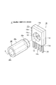
【解決手段】樹脂製基台11の一側面11a側を臨むように発光素子又は受光素子のいずれか一方の光電変換素子12が取り付けられた光電変換素子パッケージ10と、光ファイバーと結合するための光通過孔20cを円筒部20a,20b内に有し、樹脂製基台11の一側面11a側に搭載される光ファイバー結合体20とを備え、光電変換素子12と光ファイバー結合体20内に形成した光通過孔20cとが光軸Kを合わせて組み立てられた光通信モジュール1において、光電変換素子パッケージ10は、樹脂製基台11の一側面11aと対向した他側面11b側に光電変換素子12が取り付けられ、且つ、一側面11aと他側面11bとの間に光軸Kに合わせて貫通して穿設された孔11cの中心位置に光電変換素子12が配置されていることを特徴とする光通信モジュール1を提供する。
【選択図】図1
Description
前記光電変換素子パッケージは、前記樹脂製基台の一側面と対向した他側面側に前記光電変換素子が取り付けられ、且つ、前記一側面と前記他側面との間に前記光軸に合わせて貫通して穿設された孔の中心位置に前記光電変換素子が配置されていることを特徴とする光通信モジュールである。
前記光ファイバー結合体は、長尺で大径に形成し大径円筒部と、短尺で小径に形成した小径円筒部とを連接させて両筒部の内部に前記光通過孔を形成し、且つ、前記小径円筒部を前記樹脂製基台内に貫通して穿設した前記孔内に嵌合させたことを特徴とする光通信モジュールである。
前記光ファイバー結合体は、前記光通過孔内に結像レンズを設けたことを特徴とする光通信モジュールである。
図2は本発明に係る実施例の光通信モジュールを示した縦断面図、
図3(a)〜(h)は図1及び図2示した光電変換素子パッケージを製造する工程を示した工程図である。
図5は本発明に係る実施例の光通信モジュールを一部変形させた変形例の光通信モジュールを示した縦断面図である。
1’…実施例を一部変形させた変形例の光通信モジュール1、
10…光電変換素子パッケージ、
11…樹脂製基台、
11a…一側面、11b…他側面、11c…位置決め用丸孔、11d…底面、
12…光電変換素子、13…円板状配線基板、
14…リードフレーム、14a…一側面、14b…他側面、14c…リード端子、
15…矩形状配線基板、16…表面実装部品(SMD)、
17…IC集積回路部品(LSI)、18…IC用封止樹脂、
20…光ファイバー結合体、
20’…実施例を一部変形させた光ファイバー結合体、
20a…大径円筒部、20b…小径円筒部、
20c…光通過孔、20d…結像レンズ、
K…光軸。
Claims (3)
- 樹脂製基台の一側面側を臨むように発光素子又は受光素子のいずれか一方の光電変換素子が取り付けられた光電変換素子パッケージと、光ファイバーと結合するための光通過孔を円筒部内に有し、前記樹脂製基台の一側面側に搭載される光ファイバー結合体とを備え、前記光電変換素子と前記光ファイバー結合体内に形成した前記光通過孔とが光軸を合わせて組み立てられた光通信モジュールにおいて、
前記光電変換素子パッケージは、前記樹脂製基台の一側面と対向した他側面側に前記光電変換素子が取り付けられ、且つ、前記一側面と前記他側面との間に前記光軸に合わせて貫通して穿設された孔の中心位置に前記光電変換素子が配置されていることを特徴とする光通信モジュール。 - 前記光ファイバー結合体は、長尺で大径に形成し大径円筒部と、短尺で小径に形成した小径円筒部とを連接させて両筒部の内部に前記光通過孔を形成し、且つ、前記小径円筒部を前記樹脂製基台内に貫通して穿設した前記孔内に嵌合させたことを特徴とする請求項1記載の光通信モジュール。
- 前記光ファイバー結合体は、前記光通過孔内に結像レンズを設けたことを特徴とする請求項1又は請求項2記載の光通信モジュール。
Priority Applications (6)
| Application Number | Priority Date | Filing Date | Title |
|---|---|---|---|
| JP2008101809A JP2009253166A (ja) | 2008-04-09 | 2008-04-09 | 光通信モジュール |
| KR1020107023520A KR20100133444A (ko) | 2008-04-09 | 2008-12-09 | 광통신 모듈 |
| PCT/JP2008/003662 WO2009125455A1 (en) | 2008-04-09 | 2008-12-09 | Optical communication module |
| CN2008801285218A CN101999088B (zh) | 2008-04-09 | 2008-12-09 | 光通信模块 |
| US12/937,001 US8608390B2 (en) | 2008-04-09 | 2008-12-09 | Optical communication module |
| EP08873825A EP2277069A1 (en) | 2008-04-09 | 2008-12-09 | Optical communication module |
Applications Claiming Priority (1)
| Application Number | Priority Date | Filing Date | Title |
|---|---|---|---|
| JP2008101809A JP2009253166A (ja) | 2008-04-09 | 2008-04-09 | 光通信モジュール |
Publications (1)
| Publication Number | Publication Date |
|---|---|
| JP2009253166A true JP2009253166A (ja) | 2009-10-29 |
Family
ID=40419085
Family Applications (1)
| Application Number | Title | Priority Date | Filing Date |
|---|---|---|---|
| JP2008101809A Abandoned JP2009253166A (ja) | 2008-04-09 | 2008-04-09 | 光通信モジュール |
Country Status (6)
| Country | Link |
|---|---|
| US (1) | US8608390B2 (ja) |
| EP (1) | EP2277069A1 (ja) |
| JP (1) | JP2009253166A (ja) |
| KR (1) | KR20100133444A (ja) |
| CN (1) | CN101999088B (ja) |
| WO (1) | WO2009125455A1 (ja) |
Cited By (3)
| Publication number | Priority date | Publication date | Assignee | Title |
|---|---|---|---|---|
| KR101119950B1 (ko) * | 2010-09-28 | 2012-03-16 | 경북대학교 산학협력단 | 저 발산각을 가지는 led 패키지 |
| CN104730654A (zh) * | 2015-03-26 | 2015-06-24 | 厦门大学 | 一种用于塑料光纤通信光收发芯片封装结构 |
| JP2015175904A (ja) * | 2014-03-13 | 2015-10-05 | オリンパス株式会社 | 光伝送モジュールおよび光伝送モジュールの製造方法 |
Families Citing this family (10)
| Publication number | Priority date | Publication date | Assignee | Title |
|---|---|---|---|---|
| US9116262B2 (en) | 2010-04-20 | 2015-08-25 | The Johns Hopkins University | High-efficiency illumination system |
| KR101434395B1 (ko) * | 2011-09-21 | 2014-09-02 | 한국전자통신연구원 | 양방향 광 송수신 장치 |
| CN103282814B (zh) * | 2011-12-26 | 2015-02-25 | 株式会社藤仓 | 光模块 |
| JP6005362B2 (ja) * | 2012-01-19 | 2016-10-12 | 日本航空電子工業株式会社 | 光モジュール及び光伝送モジュール |
| TWI560481B (en) * | 2012-10-29 | 2016-12-01 | Hon Hai Prec Ind Co Ltd | Photoelectric converting module |
| TW201441704A (zh) * | 2013-04-17 | 2014-11-01 | Hon Hai Prec Ind Co Ltd | 光通訊模組 |
| US9733440B2 (en) * | 2014-04-29 | 2017-08-15 | Corning Incorporated | Optical connectors for coupling light sources to optical fibers |
| EP3174088B1 (en) * | 2015-11-26 | 2020-12-30 | Siyang Grande Electronics Co., Ltd. | Method of manufacturing a plastic packaged smd diode |
| CN110568571A (zh) * | 2019-10-24 | 2019-12-13 | 刘向宁 | 一种无源光纤转换装置 |
| CN113467015B (zh) * | 2021-08-03 | 2023-03-21 | 新疆师范大学 | 一种激光器耦合台的中心校准装置 |
Citations (6)
| Publication number | Priority date | Publication date | Assignee | Title |
|---|---|---|---|---|
| JPH05267694A (ja) * | 1992-03-19 | 1993-10-15 | Nec Corp | 光電変換装置 |
| JP2000277814A (ja) * | 1999-03-29 | 2000-10-06 | Sumitomo Electric Ind Ltd | 光通信モジュール |
| JP2002023025A (ja) * | 2000-07-07 | 2002-01-23 | Yazaki Corp | 光コネクタ |
| JP2002082258A (ja) * | 2000-07-03 | 2002-03-22 | Yazaki Corp | ハイブリッドコネクタの組み付け方法及びハイブリッドコネクタ |
| JP2004138966A (ja) * | 2002-10-21 | 2004-05-13 | Yazaki Corp | 一芯双方向光送受信コネクタ |
| JP2007086177A (ja) * | 2005-09-20 | 2007-04-05 | Yazaki Corp | 受発光デバイス測定装置 |
Family Cites Families (10)
| Publication number | Priority date | Publication date | Assignee | Title |
|---|---|---|---|---|
| DE3172553D1 (en) * | 1980-11-28 | 1985-11-07 | Toshiba Kk | Method for manufacturing a module for a fiber optic link |
| IT1169922B (it) | 1983-11-04 | 1987-06-03 | Telettra Lab Telefon | Sistema e dispositivi per la connessione di fotorivelatori e di fibra ottica |
| JPH02275913A (ja) | 1989-04-18 | 1990-11-09 | Sumitomo Electric Ind Ltd | 光レセプタクル |
| JP2941303B2 (ja) | 1989-05-12 | 1999-08-25 | 株式会社日立製作所 | 光フロントエンド装置 |
| EP0826997B1 (en) | 1996-08-26 | 2003-07-23 | Sumitomo Electric Industries, Ltd. | Optoelectronic module and method of manufacturing the same |
| JP3979168B2 (ja) * | 2002-04-26 | 2007-09-19 | ヤマハ株式会社 | 鍵盤楽器の押鍵検出装置における発光部構造 |
| JP2004334023A (ja) | 2003-05-09 | 2004-11-25 | Fujikura Ltd | 光モジュールおよび光触媒装置 |
| JP2006030813A (ja) | 2004-07-21 | 2006-02-02 | Citizen Electronics Co Ltd | 光ファイバモジュール |
| US7223028B2 (en) * | 2004-09-09 | 2007-05-29 | Finisar Corporation | Optical barrels with electromagnetic shielding |
| JP3955065B2 (ja) | 2005-01-18 | 2007-08-08 | シャープ株式会社 | 光結合器 |
-
2008
- 2008-04-09 JP JP2008101809A patent/JP2009253166A/ja not_active Abandoned
- 2008-12-09 US US12/937,001 patent/US8608390B2/en not_active Expired - Fee Related
- 2008-12-09 CN CN2008801285218A patent/CN101999088B/zh not_active Expired - Fee Related
- 2008-12-09 WO PCT/JP2008/003662 patent/WO2009125455A1/en not_active Ceased
- 2008-12-09 KR KR1020107023520A patent/KR20100133444A/ko not_active Ceased
- 2008-12-09 EP EP08873825A patent/EP2277069A1/en not_active Withdrawn
Patent Citations (6)
| Publication number | Priority date | Publication date | Assignee | Title |
|---|---|---|---|---|
| JPH05267694A (ja) * | 1992-03-19 | 1993-10-15 | Nec Corp | 光電変換装置 |
| JP2000277814A (ja) * | 1999-03-29 | 2000-10-06 | Sumitomo Electric Ind Ltd | 光通信モジュール |
| JP2002082258A (ja) * | 2000-07-03 | 2002-03-22 | Yazaki Corp | ハイブリッドコネクタの組み付け方法及びハイブリッドコネクタ |
| JP2002023025A (ja) * | 2000-07-07 | 2002-01-23 | Yazaki Corp | 光コネクタ |
| JP2004138966A (ja) * | 2002-10-21 | 2004-05-13 | Yazaki Corp | 一芯双方向光送受信コネクタ |
| JP2007086177A (ja) * | 2005-09-20 | 2007-04-05 | Yazaki Corp | 受発光デバイス測定装置 |
Cited By (3)
| Publication number | Priority date | Publication date | Assignee | Title |
|---|---|---|---|---|
| KR101119950B1 (ko) * | 2010-09-28 | 2012-03-16 | 경북대학교 산학협력단 | 저 발산각을 가지는 led 패키지 |
| JP2015175904A (ja) * | 2014-03-13 | 2015-10-05 | オリンパス株式会社 | 光伝送モジュールおよび光伝送モジュールの製造方法 |
| CN104730654A (zh) * | 2015-03-26 | 2015-06-24 | 厦门大学 | 一种用于塑料光纤通信光收发芯片封装结构 |
Also Published As
| Publication number | Publication date |
|---|---|
| CN101999088B (zh) | 2013-03-06 |
| EP2277069A1 (en) | 2011-01-26 |
| US20110026937A1 (en) | 2011-02-03 |
| KR20100133444A (ko) | 2010-12-21 |
| WO2009125455A1 (en) | 2009-10-15 |
| CN101999088A (zh) | 2011-03-30 |
| US8608390B2 (en) | 2013-12-17 |
Similar Documents
| Publication | Publication Date | Title |
|---|---|---|
| JP2009253166A (ja) | 光通信モジュール | |
| JP5246136B2 (ja) | 光送受信器 | |
| CN110568569A (zh) | 一种集成封装的光引擎及其信号发射、接收方法 | |
| CN101569023A (zh) | 用于光电子器件的壳体和光电子器件在壳体中的布置 | |
| CN100578764C (zh) | 光学半导体器件、光连接器以及电子设备 | |
| JP2002261265A (ja) | 光通信装置 | |
| JP2009260227A (ja) | 光電気変換装置 | |
| JP2010237640A (ja) | 光モジュールおよびモジュール付きケーブル | |
| JP4307344B2 (ja) | 表面実装型モジュール | |
| JP4269291B2 (ja) | 光モジュール | |
| JP2004286835A (ja) | 光学素子搭載装置及びその製造方法、光学素子搭載装置付き配線基板 | |
| JP2003008065A (ja) | Smd型光素子モジュールの製造方法 | |
| JP2003241028A (ja) | 光送信モジュール | |
| JP2003004987A (ja) | 光送信及び受信モジュール設置構造 | |
| JP5402786B2 (ja) | 光通信モジュールの製造方法 | |
| JP2013225011A (ja) | 光モジュール用基体及び光モジュール | |
| JP4852517B2 (ja) | 光送受信装置 | |
| JP2011003610A (ja) | 光通信モジュール | |
| US7220063B2 (en) | Optical transceiver module | |
| JPH0935594A (ja) | 光センサ | |
| TWI231108B (en) | Optical transceiver module and manufacturing method thereof | |
| JP2011197275A (ja) | 光リンクモジュール | |
| JP2008109048A (ja) | 光半導体装置及び光伝送装置 | |
| JP2013020080A (ja) | 光モジュール及びその製造方法 | |
| JP2005233995A (ja) | 光電変換プラグの製造方法 |
Legal Events
| Date | Code | Title | Description |
|---|---|---|---|
| A621 | Written request for application examination |
Free format text: JAPANESE INTERMEDIATE CODE: A621 Effective date: 20110225 |
|
| A131 | Notification of reasons for refusal |
Free format text: JAPANESE INTERMEDIATE CODE: A131 Effective date: 20130416 |
|
| A977 | Report on retrieval |
Free format text: JAPANESE INTERMEDIATE CODE: A971007 Effective date: 20130417 |
|
| A521 | Request for written amendment filed |
Free format text: JAPANESE INTERMEDIATE CODE: A523 Effective date: 20130612 |
|
| A02 | Decision of refusal |
Free format text: JAPANESE INTERMEDIATE CODE: A02 Effective date: 20130903 |
|
| A521 | Request for written amendment filed |
Free format text: JAPANESE INTERMEDIATE CODE: A523 Effective date: 20131107 |
|
| A911 | Transfer to examiner for re-examination before appeal (zenchi) |
Free format text: JAPANESE INTERMEDIATE CODE: A911 Effective date: 20131114 |
|
| A912 | Re-examination (zenchi) completed and case transferred to appeal board |
Free format text: JAPANESE INTERMEDIATE CODE: A912 Effective date: 20131129 |
|
| A762 | Written abandonment of application |
Free format text: JAPANESE INTERMEDIATE CODE: A762 Effective date: 20141003 |