JP2010141231A - 半導体装置の製造方法及び半導体装置 - Google Patents
半導体装置の製造方法及び半導体装置 Download PDFInfo
- Publication number
- JP2010141231A JP2010141231A JP2008318100A JP2008318100A JP2010141231A JP 2010141231 A JP2010141231 A JP 2010141231A JP 2008318100 A JP2008318100 A JP 2008318100A JP 2008318100 A JP2008318100 A JP 2008318100A JP 2010141231 A JP2010141231 A JP 2010141231A
- Authority
- JP
- Japan
- Prior art keywords
- groove
- semiconductor device
- film
- substrate
- manufacturing
- Prior art date
- Legal status (The legal status is an assumption and is not a legal conclusion. Google has not performed a legal analysis and makes no representation as to the accuracy of the status listed.)
- Granted
Links
Images
Classifications
-
- H—ELECTRICITY
- H10—SEMICONDUCTOR DEVICES; ELECTRIC SOLID-STATE DEVICES NOT OTHERWISE PROVIDED FOR
- H10W—GENERIC PACKAGES, INTERCONNECTIONS, CONNECTORS OR OTHER CONSTRUCTIONAL DETAILS OF DEVICES COVERED BY CLASS H10
- H10W10/00—Isolation regions in semiconductor bodies between components of integrated devices
- H10W10/01—Manufacture or treatment
- H10W10/011—Manufacture or treatment of isolation regions comprising dielectric materials
- H10W10/014—Manufacture or treatment of isolation regions comprising dielectric materials using trench refilling with dielectric materials, e.g. shallow trench isolations
-
- H—ELECTRICITY
- H10—SEMICONDUCTOR DEVICES; ELECTRIC SOLID-STATE DEVICES NOT OTHERWISE PROVIDED FOR
- H10W—GENERIC PACKAGES, INTERCONNECTIONS, CONNECTORS OR OTHER CONSTRUCTIONAL DETAILS OF DEVICES COVERED BY CLASS H10
- H10W10/00—Isolation regions in semiconductor bodies between components of integrated devices
- H10W10/01—Manufacture or treatment
- H10W10/011—Manufacture or treatment of isolation regions comprising dielectric materials
- H10W10/014—Manufacture or treatment of isolation regions comprising dielectric materials using trench refilling with dielectric materials, e.g. shallow trench isolations
- H10W10/0145—Manufacture or treatment of isolation regions comprising dielectric materials using trench refilling with dielectric materials, e.g. shallow trench isolations of trenches having shapes other than rectangular or V-shape
-
- H—ELECTRICITY
- H10—SEMICONDUCTOR DEVICES; ELECTRIC SOLID-STATE DEVICES NOT OTHERWISE PROVIDED FOR
- H10W—GENERIC PACKAGES, INTERCONNECTIONS, CONNECTORS OR OTHER CONSTRUCTIONAL DETAILS OF DEVICES COVERED BY CLASS H10
- H10W10/00—Isolation regions in semiconductor bodies between components of integrated devices
- H10W10/10—Isolation regions comprising dielectric materials
- H10W10/17—Isolation regions comprising dielectric materials formed using trench refilling with dielectric materials, e.g. shallow trench isolations
Landscapes
- Element Separation (AREA)
- Internal Circuitry In Semiconductor Integrated Circuit Devices (AREA)
Abstract
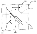
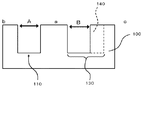
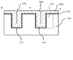
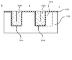
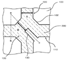
【解決手段】この半導体装置の製造方法は、基板100に第1の溝110及び第1の溝110と交差する第2の溝120を形成する工程と、基板100に対して成膜処理を行うことにより、第1の溝110内及び第2の溝120内に膜200を埋め込む工程と、基板100上に位置する膜200を除去する工程とを備える。そして第1の溝110及び第2の溝120を形成する工程において、第1の溝110と第2の溝120の交差部分130に、平面視において交差部分130の角の一つから交差部分130の中央に向けて延伸する凸部140を形成する。
【選択図】図1
Description
前記基板に対して成膜処理を行うことにより、前記第1の溝内及び前記第2の溝内に膜を埋め込む工程と、
前記基板上に位置する前記膜を除去する工程と、
を備え、
前記第1の溝及び前記第2の溝を形成する工程において、前記第1の溝と前記第2の溝の交差部分に、平面視において前記交差部分の角の一つから前記交差部分の中央に向けて延伸する凸部を形成する半導体装置の製造方法が提供される。
前記基板に形成された第1の溝と、
前記基板に形成され、前記第1の溝と交差する第2の溝と、
前記第1の溝と前記第2の溝の交差部分に形成され、平面視において前記交差部分の角の一つから前記交差部分の中央に向けて延伸する凸部と
前記第1の溝内及び前記第2の溝内に埋め込まれた膜と、
を備える半導体装置が提供される。
102 角
104 絶縁層
110 第1の溝
120 第2の溝
130 交差部分
140 凸部
200 膜
202 窪み
204 窪み
Claims (10)
- 基板に第1の溝、及び前記第1の溝と交差する第2の溝を形成する工程と、
前記基板に対して成膜処理を行うことにより、前記第1の溝内及び前記第2の溝内に膜を埋め込む工程と、
前記基板上に位置する前記膜を除去する工程と、
を備え、
前記第1の溝及び前記第2の溝を形成する工程において、前記第1の溝と前記第2の溝の交差部分に、平面視において前記交差部分の角の一つから前記交差部分の中央に向けて延伸する凸部を形成する半導体装置の製造方法。 - 請求項1に記載の半導体装置の製造方法において、
前記第1の溝及び前記第2の溝を形成する工程において、
前記第1の溝及び前記第2の溝を直交させ、
前記凸部を前記第1の溝の延伸方向に対して45°の角度で延伸させる半導体装置の製造方法。 - 請求項1又は2に記載の半導体装置の製造方法において、
前記第1の溝及び前記第2の溝を形成する工程において、
前記凸部を平面視において略長方形にして、
前記交差部分の4つの角を、前記凸部の側面のうち対向する面と平行に面取りする半導体装置の製造方法。 - 請求項3に記載の半導体装置の製造方法において、
前記第1の溝及び前記第2の溝を形成する工程において、
前記第1の溝及び前記第2の溝の幅を等しくして、
前記交差部分の4つの角それぞれを、前記凸部のうち前記角に対向する側面までの距離が前記第1の溝の幅と等しくなるように面取りする半導体装置の製造方法。 - 請求項1〜4のいずれかに記載の半導体装置の製造方法において、
前記基板はシリコン基板であり、
前記膜はポリシリコン膜であり、
前記第1の溝及び前記第2の溝を形成した後、前記膜を埋め込む工程の間に、前記第1の溝及び前記第2の溝に酸化シリコン膜を形成する工程を有する半導体装置の製造方法。 - 基板と、
前記基板に形成された第1の溝と、
前記基板に形成され、前記第1の溝と交差する第2の溝と、
前記第1の溝と前記第2の溝の交差部分に形成され、平面視において前記交差部分の角の一つから前記交差部分の中央に向けて延伸する凸部と
前記第1の溝内及び前記第2の溝内に埋め込まれた膜と、
を備える半導体装置。 - 請求項6に記載の半導体装置において、
前記第1の溝は前記第2の溝に直交しており、
平面視において、前記凸部は前記第1の溝の延伸方向に対して45°の角度で延伸する半導体装置。 - 請求項6又は7に記載の半導体装置において、
前記凸部は平面視において略長方形であり、
前記交差部分の4つの角は、前記凸部のうち前記角に対向する側面と平行に面取りされている半導体装置。 - 請求項8に記載の半導体装置において、
前記第1の溝及び前記第2の溝の幅は等しく、
前記交差部分の4つの角それぞれは、前記凸部のうち前記角に対向する側面までの距離が前記第1の溝の幅と等しくなるように面取りされている半導体装置。 - 請求項6〜9のいずれか一つに記載の半導体装置において、
前記基板はシリコン基板であり、
前記膜はポリシリコン膜であり、
前記第1の溝及び前記第2の溝の側壁及び底面は酸化シリコン膜を有する半導体装置。
Priority Applications (3)
| Application Number | Priority Date | Filing Date | Title |
|---|---|---|---|
| JP2008318100A JP5527964B2 (ja) | 2008-12-15 | 2008-12-15 | 半導体装置の製造方法及び半導体装置 |
| US12/591,932 US8377794B2 (en) | 2008-12-15 | 2009-12-04 | Method of manufacturing semiconductor device, and semiconductor device |
| CN2009102590341A CN101794728B (zh) | 2008-12-15 | 2009-12-09 | 制造半导体器件的方法和半导体器件 |
Applications Claiming Priority (1)
| Application Number | Priority Date | Filing Date | Title |
|---|---|---|---|
| JP2008318100A JP5527964B2 (ja) | 2008-12-15 | 2008-12-15 | 半導体装置の製造方法及び半導体装置 |
Publications (2)
| Publication Number | Publication Date |
|---|---|
| JP2010141231A true JP2010141231A (ja) | 2010-06-24 |
| JP5527964B2 JP5527964B2 (ja) | 2014-06-25 |
Family
ID=42239502
Family Applications (1)
| Application Number | Title | Priority Date | Filing Date |
|---|---|---|---|
| JP2008318100A Expired - Fee Related JP5527964B2 (ja) | 2008-12-15 | 2008-12-15 | 半導体装置の製造方法及び半導体装置 |
Country Status (3)
| Country | Link |
|---|---|
| US (1) | US8377794B2 (ja) |
| JP (1) | JP5527964B2 (ja) |
| CN (1) | CN101794728B (ja) |
Families Citing this family (2)
| Publication number | Priority date | Publication date | Assignee | Title |
|---|---|---|---|---|
| US9391001B2 (en) | 2013-08-26 | 2016-07-12 | Micron Technology, Inc. | Semiconductor constructions |
| KR102732446B1 (ko) * | 2020-01-17 | 2024-11-21 | 삼성전자주식회사 | 배선 구조물 및 이를 포함하는 수직형 메모리 장치 |
Citations (6)
| Publication number | Priority date | Publication date | Assignee | Title |
|---|---|---|---|---|
| JPH04264752A (ja) * | 1991-02-20 | 1992-09-21 | Fujitsu Ltd | フォトマスク及び半導体装置の製造方法 |
| JPH04274344A (ja) * | 1991-03-01 | 1992-09-30 | Matsushita Electron Corp | 半導体装置の製造方法 |
| JPH10308443A (ja) * | 1997-05-02 | 1998-11-17 | Nec Corp | 半導体集積回路装置 |
| DE102005059034A1 (de) * | 2005-12-10 | 2007-06-14 | X-Fab Semiconductor Foundries Ag | Isolationsgrabenstruktur |
| JP2008130826A (ja) * | 2006-11-21 | 2008-06-05 | Rohm Co Ltd | 半導体装置および半導体装置の製造方法 |
| DE102008029235B3 (de) * | 2008-06-19 | 2009-10-08 | X-Fab Semiconductor Foundries Ag | Kreuzungen von Isolationsgräben der SOI-Technologie |
Family Cites Families (6)
| Publication number | Priority date | Publication date | Assignee | Title |
|---|---|---|---|---|
| US5094973A (en) * | 1987-11-23 | 1992-03-10 | Texas Instrument Incorporated | Trench pillar for wafer processing |
| JPH04127148A (ja) | 1990-09-19 | 1992-04-28 | Hitachi Ltd | マスクおよびそれを用いた半導体装置の製造方法 |
| KR100249025B1 (ko) * | 1998-03-06 | 2000-03-15 | 김영환 | 반도체장치의 소자분리방법 |
| JP4127148B2 (ja) | 2003-07-14 | 2008-07-30 | 富士ゼロックス株式会社 | 画像読取装置 |
| KR100525111B1 (ko) * | 2004-04-19 | 2005-11-01 | 주식회사 하이닉스반도체 | 반도체 소자 |
| DE102005059035B4 (de) * | 2005-12-10 | 2007-11-08 | X-Fab Semiconductor Foundries Ag | Isolationsgrabenstrukturen für hohe Spannungen |
-
2008
- 2008-12-15 JP JP2008318100A patent/JP5527964B2/ja not_active Expired - Fee Related
-
2009
- 2009-12-04 US US12/591,932 patent/US8377794B2/en not_active Expired - Fee Related
- 2009-12-09 CN CN2009102590341A patent/CN101794728B/zh not_active Expired - Fee Related
Patent Citations (9)
| Publication number | Priority date | Publication date | Assignee | Title |
|---|---|---|---|---|
| JPH04264752A (ja) * | 1991-02-20 | 1992-09-21 | Fujitsu Ltd | フォトマスク及び半導体装置の製造方法 |
| JPH04274344A (ja) * | 1991-03-01 | 1992-09-30 | Matsushita Electron Corp | 半導体装置の製造方法 |
| JPH10308443A (ja) * | 1997-05-02 | 1998-11-17 | Nec Corp | 半導体集積回路装置 |
| DE102005059034A1 (de) * | 2005-12-10 | 2007-06-14 | X-Fab Semiconductor Foundries Ag | Isolationsgrabenstruktur |
| WO2007065953A1 (de) * | 2005-12-10 | 2007-06-14 | X-Fab Semiconductor Foundries Ag | Isolationsgrabenkreuzungsstruktur mit reduzierter spaltweite |
| JP2009518839A (ja) * | 2005-12-10 | 2009-05-07 | エックス−ファブ・セミコンダクター・ファウンダリーズ・アーゲー | 縮小されたスリット幅を有する絶縁トレンチ交差構造 |
| JP2008130826A (ja) * | 2006-11-21 | 2008-06-05 | Rohm Co Ltd | 半導体装置および半導体装置の製造方法 |
| DE102008029235B3 (de) * | 2008-06-19 | 2009-10-08 | X-Fab Semiconductor Foundries Ag | Kreuzungen von Isolationsgräben der SOI-Technologie |
| WO2009153356A1 (de) * | 2008-06-19 | 2009-12-23 | X-Fab Semiconductor Foundries Ag | Halbleiterbauelement mit kreuzungen von isolationsgräben |
Also Published As
| Publication number | Publication date |
|---|---|
| US8377794B2 (en) | 2013-02-19 |
| CN101794728B (zh) | 2013-05-08 |
| JP5527964B2 (ja) | 2014-06-25 |
| US20100148299A1 (en) | 2010-06-17 |
| CN101794728A (zh) | 2010-08-04 |
Similar Documents
| Publication | Publication Date | Title |
|---|---|---|
| US11158639B2 (en) | Asymmetric FinFET in memory device, method of fabricating same and semiconductor device | |
| TWI436410B (zh) | 形成積體電路結構之方法 | |
| CN101536160A (zh) | 蚀刻图案层以在其中形成交错高度的方法和中间半导体装置结构 | |
| JPH1174339A (ja) | 半導体装置及びその製造方法 | |
| CN100490080C (zh) | 半导体器件中凹陷栅极的制造方法 | |
| KR101518333B1 (ko) | 더블 패터닝 공정을 이용하는 반도체 소자의 패턴 형성 방법 | |
| JP4610323B2 (ja) | リセスチャネル領域を備えた半導体素子の製造方法 | |
| JP2007184518A (ja) | フィン構造の半導体素子の形成方法 | |
| JP2715581B2 (ja) | 半導体装置及びその製造方法 | |
| JP5527964B2 (ja) | 半導体装置の製造方法及び半導体装置 | |
| JP2006135067A (ja) | 半導体装置およびその製造方法 | |
| US10043675B2 (en) | Semiconductor device and method for fabricating the same | |
| KR100744658B1 (ko) | 플라스크형 리세스 게이트를 갖는 반도체 소자의 제조방법 | |
| JP2010118410A (ja) | 半導体装置 | |
| US20060223277A1 (en) | Method of manufacturing a semiconductor memory device | |
| KR100720258B1 (ko) | 반도체 소자의 형성 방법 | |
| KR100672765B1 (ko) | 반도체 소자의 제조 방법 | |
| JP2007027681A (ja) | 半導体素子の製造方法 | |
| JP4987244B2 (ja) | 半導体装置の製造方法 | |
| KR20140105940A (ko) | 절연막 구조물을 포함하는 반도체 소자 및 이의 제조 방법 | |
| JP2008004881A (ja) | 素子分離構造部の製造方法 | |
| CN113299738B (zh) | 半导体装置及其形成方法 | |
| JP2008130826A (ja) | 半導体装置および半導体装置の製造方法 | |
| KR100720255B1 (ko) | 반도체 소자 및 그의 형성 방법 | |
| KR20110075935A (ko) | 반도체 소자 및 그의 형성 방법 |
Legal Events
| Date | Code | Title | Description |
|---|---|---|---|
| A621 | Written request for application examination |
Free format text: JAPANESE INTERMEDIATE CODE: A621 Effective date: 20111017 |
|
| A977 | Report on retrieval |
Free format text: JAPANESE INTERMEDIATE CODE: A971007 Effective date: 20130612 |
|
| A131 | Notification of reasons for refusal |
Free format text: JAPANESE INTERMEDIATE CODE: A131 Effective date: 20130618 |
|
| A521 | Request for written amendment filed |
Free format text: JAPANESE INTERMEDIATE CODE: A523 Effective date: 20130807 |
|
| TRDD | Decision of grant or rejection written | ||
| A01 | Written decision to grant a patent or to grant a registration (utility model) |
Free format text: JAPANESE INTERMEDIATE CODE: A01 Effective date: 20140401 |
|
| A61 | First payment of annual fees (during grant procedure) |
Free format text: JAPANESE INTERMEDIATE CODE: A61 Effective date: 20140415 |
|
| R150 | Certificate of patent or registration of utility model |
Ref document number: 5527964 Country of ref document: JP Free format text: JAPANESE INTERMEDIATE CODE: R150 |
|
| S531 | Written request for registration of change of domicile |
Free format text: JAPANESE INTERMEDIATE CODE: R313531 |
|
| R350 | Written notification of registration of transfer |
Free format text: JAPANESE INTERMEDIATE CODE: R350 |
|
| LAPS | Cancellation because of no payment of annual fees |