JP2012102365A - 機能性紋様形成方法及び機能性デバイス - Google Patents
機能性紋様形成方法及び機能性デバイス Download PDFInfo
- Publication number
- JP2012102365A JP2012102365A JP2010251885A JP2010251885A JP2012102365A JP 2012102365 A JP2012102365 A JP 2012102365A JP 2010251885 A JP2010251885 A JP 2010251885A JP 2010251885 A JP2010251885 A JP 2010251885A JP 2012102365 A JP2012102365 A JP 2012102365A
- Authority
- JP
- Japan
- Prior art keywords
- pattern
- substrate
- functional
- functional pattern
- forming
- Prior art date
- Legal status (The legal status is an assumption and is not a legal conclusion. Google has not performed a legal analysis and makes no representation as to the accuracy of the status listed.)
- Granted
Links
- 238000000034 method Methods 0.000 title claims abstract description 64
- 239000000758 substrate Substances 0.000 claims abstract description 58
- 230000008569 process Effects 0.000 claims abstract description 31
- 238000007747 plating Methods 0.000 claims abstract description 27
- 239000012295 chemical reaction liquid Substances 0.000 claims abstract description 12
- 230000000694 effects Effects 0.000 claims abstract description 6
- 238000012986 modification Methods 0.000 claims abstract description 6
- 230000004048 modification Effects 0.000 claims abstract description 6
- 238000007639 printing Methods 0.000 claims abstract description 6
- 238000003825 pressing Methods 0.000 claims abstract description 5
- 230000004913 activation Effects 0.000 claims abstract description 4
- 238000012546 transfer Methods 0.000 claims abstract description 4
- 229910052751 metal Inorganic materials 0.000 claims description 35
- 239000002184 metal Substances 0.000 claims description 35
- 239000011347 resin Substances 0.000 claims description 20
- 229920005989 resin Polymers 0.000 claims description 20
- 230000007797 corrosion Effects 0.000 claims description 19
- 238000005260 corrosion Methods 0.000 claims description 19
- 239000007788 liquid Substances 0.000 claims description 14
- 230000007261 regionalization Effects 0.000 claims description 14
- 238000007772 electroless plating Methods 0.000 claims description 9
- 238000002360 preparation method Methods 0.000 claims description 5
- 238000003475 lamination Methods 0.000 claims description 3
- 238000005530 etching Methods 0.000 abstract description 10
- 239000000243 solution Substances 0.000 description 35
- 238000011282 treatment Methods 0.000 description 20
- KDLHZDBZIXYQEI-UHFFFAOYSA-N palladium Substances [Pd] KDLHZDBZIXYQEI-UHFFFAOYSA-N 0.000 description 18
- RYGMFSIKBFXOCR-UHFFFAOYSA-N Copper Chemical compound [Cu] RYGMFSIKBFXOCR-UHFFFAOYSA-N 0.000 description 17
- 229910052802 copper Inorganic materials 0.000 description 17
- 239000010949 copper Substances 0.000 description 17
- 238000006243 chemical reaction Methods 0.000 description 14
- 229920001721 polyimide Polymers 0.000 description 13
- 238000005516 engineering process Methods 0.000 description 12
- PXHVJJICTQNCMI-UHFFFAOYSA-N Nickel Chemical compound [Ni] PXHVJJICTQNCMI-UHFFFAOYSA-N 0.000 description 10
- KWYUFKZDYYNOTN-UHFFFAOYSA-M Potassium hydroxide Chemical compound [OH-].[K+] KWYUFKZDYYNOTN-UHFFFAOYSA-M 0.000 description 9
- 238000004519 manufacturing process Methods 0.000 description 9
- 238000009713 electroplating Methods 0.000 description 8
- XLYOFNOQVPJJNP-UHFFFAOYSA-N water Substances O XLYOFNOQVPJJNP-UHFFFAOYSA-N 0.000 description 7
- 239000010408 film Substances 0.000 description 6
- 239000000126 substance Substances 0.000 description 6
- 238000005406 washing Methods 0.000 description 6
- 239000004642 Polyimide Substances 0.000 description 5
- 230000006866 deterioration Effects 0.000 description 5
- 230000003628 erosive effect Effects 0.000 description 5
- 229910052759 nickel Inorganic materials 0.000 description 5
- 229910052763 palladium Inorganic materials 0.000 description 5
- 238000000206 photolithography Methods 0.000 description 5
- 239000000047 product Substances 0.000 description 5
- 238000007788 roughening Methods 0.000 description 5
- 239000002585 base Substances 0.000 description 4
- 239000003054 catalyst Substances 0.000 description 4
- 230000007774 longterm Effects 0.000 description 4
- 238000012545 processing Methods 0.000 description 4
- 239000000853 adhesive Substances 0.000 description 3
- 230000001070 adhesive effect Effects 0.000 description 3
- 230000000740 bleeding effect Effects 0.000 description 3
- 238000013461 design Methods 0.000 description 3
- 238000000813 microcontact printing Methods 0.000 description 3
- 235000011118 potassium hydroxide Nutrition 0.000 description 3
- 238000004544 sputter deposition Methods 0.000 description 3
- 239000010409 thin film Substances 0.000 description 3
- 239000007864 aqueous solution Substances 0.000 description 2
- 230000015572 biosynthetic process Effects 0.000 description 2
- 230000008859 change Effects 0.000 description 2
- 239000003795 chemical substances by application Substances 0.000 description 2
- 239000004927 clay Substances 0.000 description 2
- 238000004140 cleaning Methods 0.000 description 2
- 230000000052 comparative effect Effects 0.000 description 2
- 230000007547 defect Effects 0.000 description 2
- 238000000151 deposition Methods 0.000 description 2
- 230000008021 deposition Effects 0.000 description 2
- 238000010586 diagram Methods 0.000 description 2
- 238000002474 experimental method Methods 0.000 description 2
- 230000002209 hydrophobic effect Effects 0.000 description 2
- 238000012423 maintenance Methods 0.000 description 2
- 238000009832 plasma treatment Methods 0.000 description 2
- 238000001556 precipitation Methods 0.000 description 2
- 238000003672 processing method Methods 0.000 description 2
- 230000009467 reduction Effects 0.000 description 2
- 238000012827 research and development Methods 0.000 description 2
- 238000004381 surface treatment Methods 0.000 description 2
- 239000002562 thickening agent Substances 0.000 description 2
- 238000001771 vacuum deposition Methods 0.000 description 2
- 239000002699 waste material Substances 0.000 description 2
- HZAXFHJVJLSVMW-UHFFFAOYSA-N 2-Aminoethan-1-ol Chemical compound NCCO HZAXFHJVJLSVMW-UHFFFAOYSA-N 0.000 description 1
- 208000019901 Anxiety disease Diseases 0.000 description 1
- 241001474374 Blennius Species 0.000 description 1
- 241000280258 Dyschoriste linearis Species 0.000 description 1
- 229910021586 Nickel(II) chloride Inorganic materials 0.000 description 1
- CBENFWSGALASAD-UHFFFAOYSA-N Ozone Chemical compound [O-][O+]=O CBENFWSGALASAD-UHFFFAOYSA-N 0.000 description 1
- 229920003171 Poly (ethylene oxide) Polymers 0.000 description 1
- BQCADISMDOOEFD-UHFFFAOYSA-N Silver Chemical compound [Ag] BQCADISMDOOEFD-UHFFFAOYSA-N 0.000 description 1
- 239000004809 Teflon Substances 0.000 description 1
- 229920006362 Teflon® Polymers 0.000 description 1
- 238000004833 X-ray photoelectron spectroscopy Methods 0.000 description 1
- 230000005856 abnormality Effects 0.000 description 1
- 230000032683 aging Effects 0.000 description 1
- 239000003513 alkali Substances 0.000 description 1
- 150000005215 alkyl ethers Chemical class 0.000 description 1
- 230000036506 anxiety Effects 0.000 description 1
- QVGXLLKOCUKJST-UHFFFAOYSA-N atomic oxygen Chemical compound [O] QVGXLLKOCUKJST-UHFFFAOYSA-N 0.000 description 1
- 230000004888 barrier function Effects 0.000 description 1
- 230000015556 catabolic process Effects 0.000 description 1
- 230000003197 catalytic effect Effects 0.000 description 1
- 239000002738 chelating agent Substances 0.000 description 1
- 150000001875 compounds Chemical class 0.000 description 1
- 238000010276 construction Methods 0.000 description 1
- 238000007796 conventional method Methods 0.000 description 1
- 150000004696 coordination complex Chemical class 0.000 description 1
- 239000013256 coordination polymer Substances 0.000 description 1
- 238000006731 degradation reaction Methods 0.000 description 1
- 238000005238 degreasing Methods 0.000 description 1
- 238000011161 development Methods 0.000 description 1
- 230000018109 developmental process Effects 0.000 description 1
- 239000012153 distilled water Substances 0.000 description 1
- 238000009826 distribution Methods 0.000 description 1
- 230000007613 environmental effect Effects 0.000 description 1
- 238000007667 floating Methods 0.000 description 1
- 230000006872 improvement Effects 0.000 description 1
- 150000002739 metals Chemical class 0.000 description 1
- 239000003607 modifier Substances 0.000 description 1
- QMMRZOWCJAIUJA-UHFFFAOYSA-L nickel dichloride Chemical compound Cl[Ni]Cl QMMRZOWCJAIUJA-UHFFFAOYSA-L 0.000 description 1
- LGQLOGILCSXPEA-UHFFFAOYSA-L nickel sulfate Chemical compound [Ni+2].[O-]S([O-])(=O)=O LGQLOGILCSXPEA-UHFFFAOYSA-L 0.000 description 1
- 229910000363 nickel(II) sulfate Inorganic materials 0.000 description 1
- 150000007524 organic acids Chemical class 0.000 description 1
- 230000003647 oxidation Effects 0.000 description 1
- 238000007254 oxidation reaction Methods 0.000 description 1
- 229910052760 oxygen Inorganic materials 0.000 description 1
- 239000001301 oxygen Substances 0.000 description 1
- PIBWKRNGBLPSSY-UHFFFAOYSA-L palladium(II) chloride Chemical compound Cl[Pd]Cl PIBWKRNGBLPSSY-UHFFFAOYSA-L 0.000 description 1
- 239000002245 particle Substances 0.000 description 1
- 238000007719 peel strength test Methods 0.000 description 1
- ACVYVLVWPXVTIT-UHFFFAOYSA-M phosphinate Chemical compound [O-][PH2]=O ACVYVLVWPXVTIT-UHFFFAOYSA-M 0.000 description 1
- -1 polyoxyethylene Polymers 0.000 description 1
- 239000002244 precipitate Substances 0.000 description 1
- 238000011112 process operation Methods 0.000 description 1
- 239000005871 repellent Substances 0.000 description 1
- 230000001846 repelling effect Effects 0.000 description 1
- 150000003839 salts Chemical class 0.000 description 1
- 238000006748 scratching Methods 0.000 description 1
- 230000002393 scratching effect Effects 0.000 description 1
- 238000007650 screen-printing Methods 0.000 description 1
- 230000009291 secondary effect Effects 0.000 description 1
- 238000004904 shortening Methods 0.000 description 1
- 239000004094 surface-active agent Substances 0.000 description 1
- 238000012360 testing method Methods 0.000 description 1
Images

Classifications
-
- B—PERFORMING OPERATIONS; TRANSPORTING
- B41—PRINTING; LINING MACHINES; TYPEWRITERS; STAMPS
- B41M—PRINTING, DUPLICATING, MARKING, OR COPYING PROCESSES; COLOUR PRINTING
- B41M3/00—Printing processes to produce particular kinds of printed work, e.g. patterns
- B41M3/006—Patterns of chemical products used for a specific purpose, e.g. pesticides, perfumes, adhesive patterns; use of microencapsulated material; Printing on smoking articles
-
- C—CHEMISTRY; METALLURGY
- C23—COATING METALLIC MATERIAL; COATING MATERIAL WITH METALLIC MATERIAL; CHEMICAL SURFACE TREATMENT; DIFFUSION TREATMENT OF METALLIC MATERIAL; COATING BY VACUUM EVAPORATION, BY SPUTTERING, BY ION IMPLANTATION OR BY CHEMICAL VAPOUR DEPOSITION, IN GENERAL; INHIBITING CORROSION OF METALLIC MATERIAL OR INCRUSTATION IN GENERAL
- C23C—COATING METALLIC MATERIAL; COATING MATERIAL WITH METALLIC MATERIAL; SURFACE TREATMENT OF METALLIC MATERIAL BY DIFFUSION INTO THE SURFACE, BY CHEMICAL CONVERSION OR SUBSTITUTION; COATING BY VACUUM EVAPORATION, BY SPUTTERING, BY ION IMPLANTATION OR BY CHEMICAL VAPOUR DEPOSITION, IN GENERAL
- C23C18/00—Chemical coating by decomposition of either liquid compounds or solutions of the coating forming compounds, without leaving reaction products of surface material in the coating; Contact plating
- C23C18/16—Chemical coating by decomposition of either liquid compounds or solutions of the coating forming compounds, without leaving reaction products of surface material in the coating; Contact plating by reduction or substitution, e.g. electroless plating
- C23C18/18—Pretreatment of the material to be coated
- C23C18/20—Pretreatment of the material to be coated of organic surfaces, e.g. resins
- C23C18/22—Roughening, e.g. by etching
-
- B—PERFORMING OPERATIONS; TRANSPORTING
- B41—PRINTING; LINING MACHINES; TYPEWRITERS; STAMPS
- B41M—PRINTING, DUPLICATING, MARKING, OR COPYING PROCESSES; COLOUR PRINTING
- B41M1/00—Inking and printing with a printer's forme
- B41M1/10—Intaglio printing ; Gravure printing
-
- C—CHEMISTRY; METALLURGY
- C23—COATING METALLIC MATERIAL; COATING MATERIAL WITH METALLIC MATERIAL; CHEMICAL SURFACE TREATMENT; DIFFUSION TREATMENT OF METALLIC MATERIAL; COATING BY VACUUM EVAPORATION, BY SPUTTERING, BY ION IMPLANTATION OR BY CHEMICAL VAPOUR DEPOSITION, IN GENERAL; INHIBITING CORROSION OF METALLIC MATERIAL OR INCRUSTATION IN GENERAL
- C23C—COATING METALLIC MATERIAL; COATING MATERIAL WITH METALLIC MATERIAL; SURFACE TREATMENT OF METALLIC MATERIAL BY DIFFUSION INTO THE SURFACE, BY CHEMICAL CONVERSION OR SUBSTITUTION; COATING BY VACUUM EVAPORATION, BY SPUTTERING, BY ION IMPLANTATION OR BY CHEMICAL VAPOUR DEPOSITION, IN GENERAL
- C23C18/00—Chemical coating by decomposition of either liquid compounds or solutions of the coating forming compounds, without leaving reaction products of surface material in the coating; Contact plating
- C23C18/16—Chemical coating by decomposition of either liquid compounds or solutions of the coating forming compounds, without leaving reaction products of surface material in the coating; Contact plating by reduction or substitution, e.g. electroless plating
- C23C18/1601—Process or apparatus
- C23C18/1603—Process or apparatus coating on selected surface areas
- C23C18/1607—Process or apparatus coating on selected surface areas by direct patterning
-
- H—ELECTRICITY
- H05—ELECTRIC TECHNIQUES NOT OTHERWISE PROVIDED FOR
- H05K—PRINTED CIRCUITS; CASINGS OR CONSTRUCTIONAL DETAILS OF ELECTRIC APPARATUS; MANUFACTURE OF ASSEMBLAGES OF ELECTRICAL COMPONENTS
- H05K3/00—Apparatus or processes for manufacturing printed circuits
- H05K3/10—Apparatus or processes for manufacturing printed circuits in which conductive material is applied to the insulating support in such a manner as to form the desired conductive pattern
- H05K3/18—Apparatus or processes for manufacturing printed circuits in which conductive material is applied to the insulating support in such a manner as to form the desired conductive pattern using precipitation techniques to apply the conductive material
-
- H—ELECTRICITY
- H05—ELECTRIC TECHNIQUES NOT OTHERWISE PROVIDED FOR
- H05K—PRINTED CIRCUITS; CASINGS OR CONSTRUCTIONAL DETAILS OF ELECTRIC APPARATUS; MANUFACTURE OF ASSEMBLAGES OF ELECTRICAL COMPONENTS
- H05K3/00—Apparatus or processes for manufacturing printed circuits
- H05K3/10—Apparatus or processes for manufacturing printed circuits in which conductive material is applied to the insulating support in such a manner as to form the desired conductive pattern
- H05K3/18—Apparatus or processes for manufacturing printed circuits in which conductive material is applied to the insulating support in such a manner as to form the desired conductive pattern using precipitation techniques to apply the conductive material
- H05K3/181—Apparatus or processes for manufacturing printed circuits in which conductive material is applied to the insulating support in such a manner as to form the desired conductive pattern using precipitation techniques to apply the conductive material by electroless plating
- H05K3/182—Apparatus or processes for manufacturing printed circuits in which conductive material is applied to the insulating support in such a manner as to form the desired conductive pattern using precipitation techniques to apply the conductive material by electroless plating characterised by the patterning method
-
- H—ELECTRICITY
- H05—ELECTRIC TECHNIQUES NOT OTHERWISE PROVIDED FOR
- H05K—PRINTED CIRCUITS; CASINGS OR CONSTRUCTIONAL DETAILS OF ELECTRIC APPARATUS; MANUFACTURE OF ASSEMBLAGES OF ELECTRICAL COMPONENTS
- H05K3/00—Apparatus or processes for manufacturing printed circuits
- H05K3/38—Improvement of the adhesion between the insulating substrate and the metal
-
- H—ELECTRICITY
- H05—ELECTRIC TECHNIQUES NOT OTHERWISE PROVIDED FOR
- H05K—PRINTED CIRCUITS; CASINGS OR CONSTRUCTIONAL DETAILS OF ELECTRIC APPARATUS; MANUFACTURE OF ASSEMBLAGES OF ELECTRICAL COMPONENTS
- H05K2201/00—Indexing scheme relating to printed circuits covered by H05K1/00
- H05K2201/01—Dielectrics
- H05K2201/0137—Materials
- H05K2201/0154—Polyimide
-
- H—ELECTRICITY
- H05—ELECTRIC TECHNIQUES NOT OTHERWISE PROVIDED FOR
- H05K—PRINTED CIRCUITS; CASINGS OR CONSTRUCTIONAL DETAILS OF ELECTRIC APPARATUS; MANUFACTURE OF ASSEMBLAGES OF ELECTRICAL COMPONENTS
- H05K2203/00—Indexing scheme relating to apparatus or processes for manufacturing printed circuits covered by H05K3/00
- H05K2203/01—Tools for processing; Objects used during processing
- H05K2203/0104—Tools for processing; Objects used during processing for patterning or coating
- H05K2203/0108—Male die used for patterning, punching or transferring
-
- H—ELECTRICITY
- H05—ELECTRIC TECHNIQUES NOT OTHERWISE PROVIDED FOR
- H05K—PRINTED CIRCUITS; CASINGS OR CONSTRUCTIONAL DETAILS OF ELECTRIC APPARATUS; MANUFACTURE OF ASSEMBLAGES OF ELECTRICAL COMPONENTS
- H05K2203/00—Indexing scheme relating to apparatus or processes for manufacturing printed circuits covered by H05K3/00
- H05K2203/11—Treatments characterised by their effect, e.g. heating, cooling, roughening
- H05K2203/1163—Chemical reaction, e.g. heating solder by exothermic reaction
-
- H—ELECTRICITY
- H05—ELECTRIC TECHNIQUES NOT OTHERWISE PROVIDED FOR
- H05K—PRINTED CIRCUITS; CASINGS OR CONSTRUCTIONAL DETAILS OF ELECTRIC APPARATUS; MANUFACTURE OF ASSEMBLAGES OF ELECTRICAL COMPONENTS
- H05K3/00—Apparatus or processes for manufacturing printed circuits
- H05K3/38—Improvement of the adhesion between the insulating substrate and the metal
- H05K3/381—Improvement of the adhesion between the insulating substrate and the metal by special treatment of the substrate
Landscapes
- Chemical & Material Sciences (AREA)
- Engineering & Computer Science (AREA)
- Microelectronics & Electronic Packaging (AREA)
- Chemical Kinetics & Catalysis (AREA)
- Manufacturing & Machinery (AREA)
- General Chemical & Material Sciences (AREA)
- Materials Engineering (AREA)
- Mechanical Engineering (AREA)
- Metallurgy (AREA)
- Organic Chemistry (AREA)
- Life Sciences & Earth Sciences (AREA)
- Pest Control & Pesticides (AREA)
- Chemically Coating (AREA)
- Manufacturing Of Printed Wiring (AREA)
- Printing Methods (AREA)
Abstract
【解決手段】下地調整工程、紋様形成工程、修飾表面積層工程などを経て、基体表面上に選択的な機能性紋様を形成する方法において、当該紋様形成工程がA.当該基体と反応する反応液2を保持し、当該機能性紋様を有した凹版5を当該基体表面に当てて当該機能性紋様を転写する押圧過程、B.反応液をそのまま一定時間保持して当該基体表面の活性度を調整する活性化調整過程の2過程を経ることで、全面に表面修飾層を形成して直接に機能性紋様9を得る。基本的には鍍金後に紋様を蝕刻などしない。
【選択図】図2
Description
以下本発明では、先端的な実装基板を代表例として詳細な説明を行う。
原理的には、版5に乗せられた反応液2はその紋様で形状が限定されている為に、若干の滲み出しが有っても、正確に版5の形状を正確に写し取った表面変性層や表面粗化が達成される。
さらに本発明では、面積の非常に小さい回路パターンなどの紋様部分だけに鍍金する為に省資源であり、全面鍍金した金属を除去する余計な腐食液なども不要であることから、一層の省資源省エネとなっている。これらによるコスト低減効果も大きい。
なお、同様の手法をバイオデバイスや化学センサーなどにも適用でき、上記と同様な優れた特徴が得られることは云うまでも無い。
ポリイミド表面を加水分解する腐蝕液の増粘剤の量や種類を変えて、粘度を水のような1cpsからゆるい粘土の様な数万cpsまで作成して実験を行った。幅70〜100ミクロン長さ3mmの線状の巾を計測した結果を表1に示す。なお、粘土状のように固い場合は、現実には印刷できなかったので除外している。
なお、紋様の剥離強度は、実施例1と同じように約0.4N/mmであり高い値を示した。
同時に得られた10x30mm角の紋様を150度で熱処理した後に剥離強度を測定したところ、約0.6〜0,8N/mmと非常に高い値を示した。一般に報告されているスパッタ−法での剥離強度に遜色無く、非常に高強度であることが判明した。これは界面のニッケルの接着強度が高いことに因ると推定される。
また、ニッケルは耐酸化性があり、酸素や水分の効果的なバリアーにもなるために、銅界面の安定性が増すので、長期信頼性の向上が期待される。
事実、150℃200時間の高温処理後も0.55N/mm以上の高い値を保持しており、長期信頼性が確認された。
(比較例1)
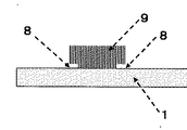
銅鍍金された50ミクロン線状の試料をTEMで断面観察を行ったところ、サイドエッチの為に、銅と基体のポリイミド界面に腐蝕による食い込み、アンダーエッチが全般に見られ、一部には深く入っているのが見られた。フォトリソ後に強いエッチングを施したところ数ミクロンの食い込みが見られた。概念図を図3に示す。
一方、実施例1の試料では、基体のポリイミドとの界面は、端部から端部まで全く異常が無く整合していることが判明した。製造工程を考えれば当然といえる。
さらに細い線になれば、比較例の試料では、線が浮き上がり剥がれると思われる。
実施例2−3についても、同じ様にTEM観察したところ、いずれも界面の整合性は良好であることが確認された。これも製造工程からして当然といえる結果である。
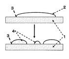
2 腐食液
3 接触角
4 水玉
5 版(スタンパー)
6 変性層
7 紋様
8 アンダーカット
9 配線
Claims (3)
- 下地調整工程、紋様形成工程、修飾表面積層工程を少なくとも含み、基体表面上に選択的な機能性紋様を形成する方法において、当該紋様形成工程がA.当該基体と反応する反応液を保持し、当該機能性紋様を有した凹版を当該基体表面に当てて当該機能性紋様を転写する押圧過程、B.反応液をそのまま一定時間保持して当該基体表面の活性度を調整する活性化調整過程の2過程を含むことを特徴とした機能性紋様形成方法及び機能性デバイス
- 鍍金下地調整工程、紋様形成工程、無電解鍍金工程を少なくとも含み、絶縁性樹脂基体表面上に選択的な導電性金属紋様を形成する方法において、当該紋様形成工程がA.当該樹脂腐蝕性を持つ腐蝕液を含有する反応液を保持し、当該機能性紋様を有した凹版を当該基体表面に当てて当該導電性金属機能性紋様を転写する押圧過程、B.反応液をそのまま一定時間保持して当該樹脂表面を僅かに当該紋様状に腐蝕する腐蝕過程の2過程を含む紋様腐蝕工程を少なくとも経ることを特徴とした導電性金属紋様形成方法及び電子電気デバイス
- 下地調整工程、紋様形成工程、修飾表面積層工程を少なくとも含み、基体表面上に選択的な機能性紋様を形成する方法において、一旦形成した表面修飾積層からなる機能性紋様上に、さらに重ねて当該表面修飾積層の腐蝕液を選択的紋様に印刷して一部の表面修飾積層からなる機能性紋様を腐蝕除去して基体表面上に選択的な機能性紋様を形成することを特徴とした電子電気デバイス
Priority Applications (4)
| Application Number | Priority Date | Filing Date | Title |
|---|---|---|---|
| JP2010251885A JP5775683B2 (ja) | 2010-11-10 | 2010-11-10 | 導電性金属紋様形成方法及び電子電気デバイス |
| KR1020137012308A KR20140020831A (ko) | 2010-11-10 | 2011-11-07 | 기능성 문양 형성 방법 및 기능성 디바이스 |
| CN2011800536333A CN103221578A (zh) | 2010-11-10 | 2011-11-07 | 功能性花纹形成方法以及功能性设备 |
| PCT/JP2011/075568 WO2012063768A1 (ja) | 2010-11-10 | 2011-11-07 | 機能性紋様形成方法及び機能性デバイス |
Applications Claiming Priority (1)
| Application Number | Priority Date | Filing Date | Title |
|---|---|---|---|
| JP2010251885A JP5775683B2 (ja) | 2010-11-10 | 2010-11-10 | 導電性金属紋様形成方法及び電子電気デバイス |
Publications (2)
| Publication Number | Publication Date |
|---|---|
| JP2012102365A true JP2012102365A (ja) | 2012-05-31 |
| JP5775683B2 JP5775683B2 (ja) | 2015-09-09 |
Family
ID=46050914
Family Applications (1)
| Application Number | Title | Priority Date | Filing Date |
|---|---|---|---|
| JP2010251885A Active JP5775683B2 (ja) | 2010-11-10 | 2010-11-10 | 導電性金属紋様形成方法及び電子電気デバイス |
Country Status (4)
| Country | Link |
|---|---|
| JP (1) | JP5775683B2 (ja) |
| KR (1) | KR20140020831A (ja) |
| CN (1) | CN103221578A (ja) |
| WO (1) | WO2012063768A1 (ja) |
Citations (13)
| Publication number | Priority date | Publication date | Assignee | Title |
|---|---|---|---|---|
| JPS58194922A (ja) * | 1982-05-08 | 1983-11-14 | Pioneer Electronic Corp | プラスチツクの部分メツキ方法 |
| JPS63182110A (ja) * | 1987-01-23 | 1988-07-27 | Mitsubishi Plastics Ind Ltd | プラスチツク表面への金属膜形成法 |
| JPH0369396A (ja) * | 1989-08-08 | 1991-03-25 | Toppan Printing Co Ltd | 凹版印刷用基板及びその製造方法 |
| JPH04193956A (ja) * | 1990-11-28 | 1992-07-14 | Sumitomo Metal Mining Co Ltd | ポリイミド樹脂のエッチング法 |
| JPH0797467A (ja) * | 1993-09-29 | 1995-04-11 | Sakae Denshi Kogyo Kk | 無極性樹脂用表面処理剤 |
| JPH10335831A (ja) * | 1997-05-23 | 1998-12-18 | Samsung Aerospace Ind Ltd | 多層プリント配線板及び該製造方法 |
| JPH11354922A (ja) * | 1998-06-05 | 1999-12-24 | Toagosei Co Ltd | 多層プリント配線板の製造方法 |
| JP2001071620A (ja) * | 1999-09-02 | 2001-03-21 | Printing Bureau Ministry Of Finance Japan | 画像形成体とその作製方法 |
| JP2004323946A (ja) * | 2003-04-28 | 2004-11-18 | New Industry Research Organization | 液相析出法によるマイクロパターニング方法 |
| JP2005129766A (ja) * | 2003-10-24 | 2005-05-19 | Nec Tokin Corp | プリント回路基板及びその製造方法 |
| JP2005241854A (ja) * | 2004-02-25 | 2005-09-08 | Seiko Epson Corp | パターン形成方法、カラーフィルタの製造方法、電気光学装置の製造方法、カラーフィルタ、電気光学装置、及び電子機器 |
| JP2010525961A (ja) * | 2007-03-22 | 2010-07-29 | イー・アイ・デュポン・ドウ・ヌムール・アンド・カンパニー | スタンプの表面を処理することにより、基板上に機能材料のパターンを形成する方法 |
| JP2010532080A (ja) * | 2007-07-04 | 2010-09-30 | コーニンクレッカ フィリップス エレクトロニクス エヌ ヴィ | パターン化された層を基板上に形成する方法 |
Family Cites Families (1)
| Publication number | Priority date | Publication date | Assignee | Title |
|---|---|---|---|---|
| CN1181985C (zh) * | 2003-03-10 | 2004-12-29 | 上海恒昊玻璃技术有限公司 | 用透光立体图案玻璃镀镜的生产方法 |
-
2010
- 2010-11-10 JP JP2010251885A patent/JP5775683B2/ja active Active
-
2011
- 2011-11-07 WO PCT/JP2011/075568 patent/WO2012063768A1/ja not_active Ceased
- 2011-11-07 CN CN2011800536333A patent/CN103221578A/zh active Pending
- 2011-11-07 KR KR1020137012308A patent/KR20140020831A/ko not_active Withdrawn
Patent Citations (13)
| Publication number | Priority date | Publication date | Assignee | Title |
|---|---|---|---|---|
| JPS58194922A (ja) * | 1982-05-08 | 1983-11-14 | Pioneer Electronic Corp | プラスチツクの部分メツキ方法 |
| JPS63182110A (ja) * | 1987-01-23 | 1988-07-27 | Mitsubishi Plastics Ind Ltd | プラスチツク表面への金属膜形成法 |
| JPH0369396A (ja) * | 1989-08-08 | 1991-03-25 | Toppan Printing Co Ltd | 凹版印刷用基板及びその製造方法 |
| JPH04193956A (ja) * | 1990-11-28 | 1992-07-14 | Sumitomo Metal Mining Co Ltd | ポリイミド樹脂のエッチング法 |
| JPH0797467A (ja) * | 1993-09-29 | 1995-04-11 | Sakae Denshi Kogyo Kk | 無極性樹脂用表面処理剤 |
| JPH10335831A (ja) * | 1997-05-23 | 1998-12-18 | Samsung Aerospace Ind Ltd | 多層プリント配線板及び該製造方法 |
| JPH11354922A (ja) * | 1998-06-05 | 1999-12-24 | Toagosei Co Ltd | 多層プリント配線板の製造方法 |
| JP2001071620A (ja) * | 1999-09-02 | 2001-03-21 | Printing Bureau Ministry Of Finance Japan | 画像形成体とその作製方法 |
| JP2004323946A (ja) * | 2003-04-28 | 2004-11-18 | New Industry Research Organization | 液相析出法によるマイクロパターニング方法 |
| JP2005129766A (ja) * | 2003-10-24 | 2005-05-19 | Nec Tokin Corp | プリント回路基板及びその製造方法 |
| JP2005241854A (ja) * | 2004-02-25 | 2005-09-08 | Seiko Epson Corp | パターン形成方法、カラーフィルタの製造方法、電気光学装置の製造方法、カラーフィルタ、電気光学装置、及び電子機器 |
| JP2010525961A (ja) * | 2007-03-22 | 2010-07-29 | イー・アイ・デュポン・ドウ・ヌムール・アンド・カンパニー | スタンプの表面を処理することにより、基板上に機能材料のパターンを形成する方法 |
| JP2010532080A (ja) * | 2007-07-04 | 2010-09-30 | コーニンクレッカ フィリップス エレクトロニクス エヌ ヴィ | パターン化された層を基板上に形成する方法 |
Also Published As
| Publication number | Publication date |
|---|---|
| CN103221578A (zh) | 2013-07-24 |
| JP5775683B2 (ja) | 2015-09-09 |
| KR20140020831A (ko) | 2014-02-19 |
| WO2012063768A1 (ja) | 2012-05-18 |
Similar Documents
| Publication | Publication Date | Title |
|---|---|---|
| JP4605409B2 (ja) | アルミニウム又はアルミニウム合金の表面処理方法 | |
| JP5835947B2 (ja) | 金属膜パターンが形成された樹脂基材 | |
| CN101479405B (zh) | 无电解镀Ni-P的方法和电子部件用基板 | |
| EP0884934A2 (en) | Substrate and method for producing it | |
| JP2012026029A (ja) | アルミニウム酸化皮膜用除去液及びアルミニウム又はアルミニウム合金の表面処理方法 | |
| CN105121700A (zh) | 立体导电图案结构体的制造方法及用于其的立体成型用材料 | |
| JP2008231459A (ja) | ポリイミド樹脂上への導電性皮膜の形成方法 | |
| JP4429141B2 (ja) | エッチング液セット、これを用いるエッチング方法及び配線基板の製造方法 | |
| JP6236824B2 (ja) | プリント配線基板の製造方法 | |
| JP2009530502A (ja) | ポリイミド基板及びそれを使用するプリント基板の製造方法 | |
| JP2020124919A (ja) | 膜形成基材 | |
| JP5775683B2 (ja) | 導電性金属紋様形成方法及び電子電気デバイス | |
| JP5775684B2 (ja) | 導電性金属紋様形成方法及び電子電気素子 | |
| JP2014534347A (ja) | 銅および銅合金をエッチングするための水性組成物 | |
| TW202231926A (zh) | 銀用蝕刻液、及使用其之印刷配線板之製造方法 | |
| JP2009161788A (ja) | めっき方法及びその方法に用いられるめっき前処理液。 | |
| JP2005179695A (ja) | 配線基板および電気配線の形成方法 | |
| JP4975344B2 (ja) | めっき方法 | |
| JP2011114241A (ja) | 配線基板の製造方法 | |
| JP2007214338A (ja) | 片面ポリイミド配線基板の製造方法 | |
| JP2014072198A (ja) | 金属パターンが形成されたポリイミド樹脂基材の製造方法 | |
| JP2024051805A (ja) | 酸化スズ膜用エッチング液 | |
| CN121137737A (zh) | 一种基于石墨烯的图形化金属膜制备方法 | |
| CN120485779A (zh) | 一种铝箔材料柔性电路板多元化学镀层工艺 | |
| CN121865531A (zh) | 一种车载印制板及提高其金手指表面达因值的加工方法 |
Legal Events
| Date | Code | Title | Description |
|---|---|---|---|
| A625 | Written request for application examination (by other person) |
Free format text: JAPANESE INTERMEDIATE CODE: A625 Effective date: 20131107 |
|
| A711 | Notification of change in applicant |
Free format text: JAPANESE INTERMEDIATE CODE: A711 Effective date: 20131217 |
|
| A131 | Notification of reasons for refusal |
Free format text: JAPANESE INTERMEDIATE CODE: A131 Effective date: 20141006 |
|
| A521 | Written amendment |
Free format text: JAPANESE INTERMEDIATE CODE: A523 Effective date: 20141203 |
|
| TRDD | Decision of grant or rejection written | ||
| A01 | Written decision to grant a patent or to grant a registration (utility model) |
Free format text: JAPANESE INTERMEDIATE CODE: A01 Effective date: 20150608 |
|
| A61 | First payment of annual fees (during grant procedure) |
Free format text: JAPANESE INTERMEDIATE CODE: A61 Effective date: 20150706 |
|
| R150 | Certificate of patent or registration of utility model |
Ref document number: 5775683 Country of ref document: JP Free format text: JAPANESE INTERMEDIATE CODE: R150 |
|
| R250 | Receipt of annual fees |
Free format text: JAPANESE INTERMEDIATE CODE: R250 |
|
| R250 | Receipt of annual fees |
Free format text: JAPANESE INTERMEDIATE CODE: R250 |