JP2012129341A - チップサーミスタ - Google Patents
チップサーミスタ Download PDFInfo
- Publication number
- JP2012129341A JP2012129341A JP2010279008A JP2010279008A JP2012129341A JP 2012129341 A JP2012129341 A JP 2012129341A JP 2010279008 A JP2010279008 A JP 2010279008A JP 2010279008 A JP2010279008 A JP 2010279008A JP 2012129341 A JP2012129341 A JP 2012129341A
- Authority
- JP
- Japan
- Prior art keywords
- thermistor
- chip
- pair
- conductor
- conductor portions
- Prior art date
- Legal status (The legal status is an assumption and is not a legal conclusion. Google has not performed a legal analysis and makes no representation as to the accuracy of the status listed.)
- Granted
Links
- 239000004020 conductor Substances 0.000 claims abstract description 122
- 229910052751 metal Inorganic materials 0.000 claims abstract description 15
- 239000002184 metal Substances 0.000 claims abstract description 15
- 239000011521 glass Substances 0.000 claims abstract description 11
- 229910044991 metal oxide Inorganic materials 0.000 claims abstract description 9
- 150000004706 metal oxides Chemical class 0.000 claims abstract description 9
- 239000000919 ceramic Substances 0.000 claims abstract description 8
- 238000007747 plating Methods 0.000 claims description 23
- 239000010410 layer Substances 0.000 description 62
- 230000035939 shock Effects 0.000 description 10
- 238000000034 method Methods 0.000 description 8
- 239000000843 powder Substances 0.000 description 7
- 229910000679 solder Inorganic materials 0.000 description 7
- 230000017525 heat dissipation Effects 0.000 description 5
- 238000004519 manufacturing process Methods 0.000 description 5
- 239000000463 material Substances 0.000 description 5
- 239000002002 slurry Substances 0.000 description 5
- 239000011230 binding agent Substances 0.000 description 4
- 238000001514 detection method Methods 0.000 description 4
- 238000010586 diagram Methods 0.000 description 4
- 238000010438 heat treatment Methods 0.000 description 4
- 239000000203 mixture Substances 0.000 description 4
- 230000008569 process Effects 0.000 description 4
- 239000000758 substrate Substances 0.000 description 3
- 229910004298 SiO 2 Inorganic materials 0.000 description 2
- 238000010521 absorption reaction Methods 0.000 description 2
- 229910052782 aluminium Inorganic materials 0.000 description 2
- 239000005388 borosilicate glass Substances 0.000 description 2
- 229910052791 calcium Inorganic materials 0.000 description 2
- 229910052802 copper Inorganic materials 0.000 description 2
- 238000007606 doctor blade method Methods 0.000 description 2
- 230000000694 effects Effects 0.000 description 2
- 238000005516 engineering process Methods 0.000 description 2
- 238000010304 firing Methods 0.000 description 2
- 229910052742 iron Inorganic materials 0.000 description 2
- 238000002844 melting Methods 0.000 description 2
- 230000008018 melting Effects 0.000 description 2
- 230000004048 modification Effects 0.000 description 2
- 238000012986 modification Methods 0.000 description 2
- 229910052759 nickel Inorganic materials 0.000 description 2
- -1 polyethylene terephthalate Polymers 0.000 description 2
- 229920000139 polyethylene terephthalate Polymers 0.000 description 2
- 239000005020 polyethylene terephthalate Substances 0.000 description 2
- 229910052596 spinel Inorganic materials 0.000 description 2
- 239000011029 spinel Substances 0.000 description 2
- 229910052726 zirconium Inorganic materials 0.000 description 2
- 229910018072 Al 2 O 3 Inorganic materials 0.000 description 1
- 230000008901 benefit Effects 0.000 description 1
- 238000009529 body temperature measurement Methods 0.000 description 1
- 238000009713 electroplating Methods 0.000 description 1
- 229910052737 gold Inorganic materials 0.000 description 1
- 229910052745 lead Inorganic materials 0.000 description 1
- 229910052748 manganese Inorganic materials 0.000 description 1
- 229910052763 palladium Inorganic materials 0.000 description 1
- 238000005498 polishing Methods 0.000 description 1
- 229910052761 rare earth metal Inorganic materials 0.000 description 1
- 150000002910 rare earth metals Chemical class 0.000 description 1
- 230000001105 regulatory effect Effects 0.000 description 1
- 230000004044 response Effects 0.000 description 1
- 230000004043 responsiveness Effects 0.000 description 1
- 238000007650 screen-printing Methods 0.000 description 1
- 239000004065 semiconductor Substances 0.000 description 1
- 229910052709 silver Inorganic materials 0.000 description 1
- 239000002356 single layer Substances 0.000 description 1
- 238000004544 sputter deposition Methods 0.000 description 1
Images


Landscapes
- Thermistors And Varistors (AREA)
Abstract
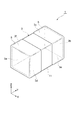
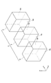
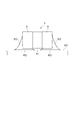
【解決手段】チップサーミスタ1は、金属酸化物を主成分とするセラミックスからなるサーミスタ部7と、金属とガラス成分とを含み且つサーミスタ部7を挟むようにサーミスタ部7の両側に配置されてサーミスタ部7と接続されている一対の導体部9と、を備えている。サーミスタ部7と一対の導体部9とは、一対の導体部9の対向方向に直交する断面形状が一対の導体部9の対向方向にわたって同じである。
【選択図】図3
Description
R=(a*ρ*t)/S
の関係式で求められる。ここで、「a」は係数であり、「ρ」はサーミスタ材料の比抵抗値であり、「t」は電極間の距離であり、「S」は電極の重なり面積である。
Claims (5)
- 金属酸化物を主成分とするセラミックスからなるサーミスタ部と、
金属とガラス成分とを含み且つ前記サーミスタ部を挟むように前記サーミスタ部の両側に配置されて前記サーミスタ部と接続されている一対の導体部と、を備え、
前記サーミスタ部と前記一対の導体部とは、前記一対の導体部の対向方向に直交する断面形状が前記一対の導体部の対向方向にわたって同じであることを特徴とするチップサーミスタ。 - 前記一対の導体部の外表面が、めっき層で覆われていることを特徴とする請求項1に記載のチップサーミスタ。
- 前記サーミスタ部は、前記一対の導体部の前記対向方向が積層方向となるように層状に形成されていることを特徴とする請求項1又は2に記載のチップサーミスタ。
- 前記一対の導体部それぞれは、前記一対の導体部の前記対向方向が積層方向となるように層状に形成されていることを特徴とする請求項1〜3のいずれか一項に記載のチップサーミスタ。
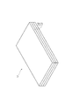
- 前記サーミスタ部の外表面が、絶縁層で覆われていることを特徴とする請求項1〜4の何れか一項に記載のチップサーミスタ。
Priority Applications (1)
| Application Number | Priority Date | Filing Date | Title |
|---|---|---|---|
| JP2010279008A JP5240286B2 (ja) | 2010-12-15 | 2010-12-15 | チップサーミスタ及びチップサーミスタの製造方法 |
Applications Claiming Priority (1)
| Application Number | Priority Date | Filing Date | Title |
|---|---|---|---|
| JP2010279008A JP5240286B2 (ja) | 2010-12-15 | 2010-12-15 | チップサーミスタ及びチップサーミスタの製造方法 |
Publications (2)
| Publication Number | Publication Date |
|---|---|
| JP2012129341A true JP2012129341A (ja) | 2012-07-05 |
| JP5240286B2 JP5240286B2 (ja) | 2013-07-17 |
Family
ID=46646077
Family Applications (1)
| Application Number | Title | Priority Date | Filing Date |
|---|---|---|---|
| JP2010279008A Expired - Fee Related JP5240286B2 (ja) | 2010-12-15 | 2010-12-15 | チップサーミスタ及びチップサーミスタの製造方法 |
Country Status (1)
| Country | Link |
|---|---|
| JP (1) | JP5240286B2 (ja) |
Cited By (3)
| Publication number | Priority date | Publication date | Assignee | Title |
|---|---|---|---|---|
| JP2018535413A (ja) * | 2015-11-02 | 2018-11-29 | エプコス アクチエンゲゼルシャフトEpcos Ag | センサ素子およびセンサ素子を製造するための方法 |
| JP2022140662A (ja) * | 2020-10-06 | 2022-09-26 | セイコーエプソン株式会社 | 振動デバイス、電子機器及び移動体 |
| US11979138B2 (en) | 2014-07-30 | 2024-05-07 | Seiko Epson Corporation | Resonator device, electronic device, and moving object |
Citations (5)
| Publication number | Priority date | Publication date | Assignee | Title |
|---|---|---|---|---|
| JPH04247603A (ja) * | 1991-02-04 | 1992-09-03 | Murata Mfg Co Ltd | Ntcサーミスタ素子の製造方法 |
| JPH05335113A (ja) * | 1992-06-03 | 1993-12-17 | Tdk Corp | サーミスタ及びその製造方法 |
| JPH06151110A (ja) * | 1992-11-11 | 1994-05-31 | Rohm Co Ltd | 面実装用ntcサーミスタ |
| JP2000082607A (ja) * | 1998-09-04 | 2000-03-21 | Mitsubishi Materials Corp | チップ型サーミスタ及びその製造方法 |
| JP2007141881A (ja) * | 2005-11-14 | 2007-06-07 | Oizumi Seisakusho:Kk | サーミスタの電極構造 |
-
2010
- 2010-12-15 JP JP2010279008A patent/JP5240286B2/ja not_active Expired - Fee Related
Patent Citations (5)
| Publication number | Priority date | Publication date | Assignee | Title |
|---|---|---|---|---|
| JPH04247603A (ja) * | 1991-02-04 | 1992-09-03 | Murata Mfg Co Ltd | Ntcサーミスタ素子の製造方法 |
| JPH05335113A (ja) * | 1992-06-03 | 1993-12-17 | Tdk Corp | サーミスタ及びその製造方法 |
| JPH06151110A (ja) * | 1992-11-11 | 1994-05-31 | Rohm Co Ltd | 面実装用ntcサーミスタ |
| JP2000082607A (ja) * | 1998-09-04 | 2000-03-21 | Mitsubishi Materials Corp | チップ型サーミスタ及びその製造方法 |
| JP2007141881A (ja) * | 2005-11-14 | 2007-06-07 | Oizumi Seisakusho:Kk | サーミスタの電極構造 |
Cited By (7)
| Publication number | Priority date | Publication date | Assignee | Title |
|---|---|---|---|---|
| US11979138B2 (en) | 2014-07-30 | 2024-05-07 | Seiko Epson Corporation | Resonator device, electronic device, and moving object |
| US12278615B2 (en) | 2014-07-30 | 2025-04-15 | Seiko Epson Corporation | Resonator device, electronic device, and moving object |
| JP2018535413A (ja) * | 2015-11-02 | 2018-11-29 | エプコス アクチエンゲゼルシャフトEpcos Ag | センサ素子およびセンサ素子を製造するための方法 |
| US10788377B2 (en) | 2015-11-02 | 2020-09-29 | Epcos Ag | Sensor element and method for producing a sensor element |
| US10908030B2 (en) | 2015-11-02 | 2021-02-02 | Epcos Ag | Sensor element and method for producing a sensor element |
| JP2022140662A (ja) * | 2020-10-06 | 2022-09-26 | セイコーエプソン株式会社 | 振動デバイス、電子機器及び移動体 |
| JP7501577B2 (ja) | 2020-10-06 | 2024-06-18 | セイコーエプソン株式会社 | 振動デバイス、電子機器及び移動体 |
Also Published As
| Publication number | Publication date |
|---|---|
| JP5240286B2 (ja) | 2013-07-17 |
Similar Documents
| Publication | Publication Date | Title |
|---|---|---|
| TWI517186B (zh) | Thermistor and its manufacturing method | |
| KR100312735B1 (ko) | 칩 써미스터 및 이의 제조방법 | |
| KR102112107B1 (ko) | 전자부품 및 전자부품의 제조 방법 | |
| JP5422052B2 (ja) | チップサーミスタ及びその製造方法 | |
| WO2012070336A1 (ja) | チップサーミスタ及びサーミスタ集合基板 | |
| JP5324390B2 (ja) | 積層電子部品 | |
| JP2013070108A (ja) | チップ抵抗器 | |
| US20080308312A1 (en) | Ceramic electronic component | |
| JP2011165752A (ja) | チップ抵抗器 | |
| JP5240286B2 (ja) | チップサーミスタ及びチップサーミスタの製造方法 | |
| JP3736602B2 (ja) | チップ型サーミスタ | |
| WO2014109224A1 (ja) | チップ抵抗器 | |
| JPH10312933A (ja) | 積層セラミック電子部品 | |
| KR20140046301A (ko) | 적층 세라믹 전자부품 및 이의 제조방법 | |
| KR101892751B1 (ko) | 칩 저항기 및 그 제조 방법 | |
| WO2021065807A1 (ja) | Ntcサーミスタ素子 | |
| JP5012432B2 (ja) | セラミック電子部品 | |
| JP2022012055A (ja) | 抵抗器 | |
| JP5929998B2 (ja) | チップサーミスタ | |
| JP2005303160A (ja) | 積層型半導体セラミック電子部品 | |
| KR20140148157A (ko) | 적층 세라믹 전자 부품의 제조 방법 및 이를 이용하여 제조된 적층 세라믹 전자 부품 | |
| CN114284115B (zh) | 复合保护器件及其制备方法 | |
| JP2008270391A (ja) | 積層型チップバリスタおよびその製造方法 | |
| JP5304772B2 (ja) | チップバリスタ及びチップバリスタの製造方法 | |
| JP2023056119A (ja) | 保護機能付き基体、電子デバイス及び電子回路基板 |
Legal Events
| Date | Code | Title | Description |
|---|---|---|---|
| A977 | Report on retrieval |
Free format text: JAPANESE INTERMEDIATE CODE: A971007 Effective date: 20121207 |
|
| A131 | Notification of reasons for refusal |
Free format text: JAPANESE INTERMEDIATE CODE: A131 Effective date: 20121211 |
|
| A521 | Request for written amendment filed |
Free format text: JAPANESE INTERMEDIATE CODE: A523 Effective date: 20130129 |
|
| TRDD | Decision of grant or rejection written | ||
| A01 | Written decision to grant a patent or to grant a registration (utility model) |
Free format text: JAPANESE INTERMEDIATE CODE: A01 Effective date: 20130305 |
|
| A61 | First payment of annual fees (during grant procedure) |
Free format text: JAPANESE INTERMEDIATE CODE: A61 Effective date: 20130318 |
|
| FPAY | Renewal fee payment (event date is renewal date of database) |
Free format text: PAYMENT UNTIL: 20160412 Year of fee payment: 3 |
|
| R150 | Certificate of patent or registration of utility model |
Free format text: JAPANESE INTERMEDIATE CODE: R150 Ref document number: 5240286 Country of ref document: JP Free format text: JAPANESE INTERMEDIATE CODE: R150 |
|
| LAPS | Cancellation because of no payment of annual fees |