JP2012131229A - 印写リソグラフィの方法 - Google Patents
印写リソグラフィの方法 Download PDFInfo
- Publication number
- JP2012131229A JP2012131229A JP2011286258A JP2011286258A JP2012131229A JP 2012131229 A JP2012131229 A JP 2012131229A JP 2011286258 A JP2011286258 A JP 2011286258A JP 2011286258 A JP2011286258 A JP 2011286258A JP 2012131229 A JP2012131229 A JP 2012131229A
- Authority
- JP
- Japan
- Prior art keywords
- template
- layer
- absorbing material
- printing
- heat absorbing
- Prior art date
- Legal status (The legal status is an assumption and is not a legal conclusion. Google has not performed a legal analysis and makes no representation as to the accuracy of the status listed.)
- Granted
Links
- 238000001459 lithography Methods 0.000 title claims abstract description 46
- 238000000034 method Methods 0.000 title claims abstract description 45
- 239000000758 substrate Substances 0.000 claims abstract description 60
- 229910052751 metal Inorganic materials 0.000 claims abstract description 40
- 239000002184 metal Substances 0.000 claims abstract description 40
- 238000012546 transfer Methods 0.000 claims abstract description 18
- 238000010438 heat treatment Methods 0.000 claims abstract description 5
- 238000007639 printing Methods 0.000 claims description 93
- 239000011358 absorbing material Substances 0.000 claims description 29
- 239000000463 material Substances 0.000 claims description 28
- 230000005855 radiation Effects 0.000 claims description 21
- PXHVJJICTQNCMI-UHFFFAOYSA-N Nickel Chemical compound [Ni] PXHVJJICTQNCMI-UHFFFAOYSA-N 0.000 claims description 10
- VYZAMTAEIAYCRO-UHFFFAOYSA-N Chromium Chemical compound [Cr] VYZAMTAEIAYCRO-UHFFFAOYSA-N 0.000 claims description 5
- 229910052804 chromium Inorganic materials 0.000 claims description 5
- 239000011651 chromium Substances 0.000 claims description 5
- 229910052759 nickel Inorganic materials 0.000 claims description 5
- 229910052782 aluminium Inorganic materials 0.000 claims description 4
- XAGFODPZIPBFFR-UHFFFAOYSA-N aluminium Chemical compound [Al] XAGFODPZIPBFFR-UHFFFAOYSA-N 0.000 claims description 4
- 230000001678 irradiating effect Effects 0.000 claims description 4
- 229920005989 resin Polymers 0.000 abstract description 37
- 239000011347 resin Substances 0.000 abstract description 37
- 229920001187 thermosetting polymer Polymers 0.000 abstract description 10
- 229920005992 thermoplastic resin Polymers 0.000 abstract description 7
- 229920001169 thermoplastic Polymers 0.000 abstract description 5
- 239000004416 thermosoftening plastic Substances 0.000 abstract description 3
- 239000010410 layer Substances 0.000 description 68
- 230000008569 process Effects 0.000 description 28
- 238000005530 etching Methods 0.000 description 10
- 230000009477 glass transition Effects 0.000 description 8
- 239000007788 liquid Substances 0.000 description 8
- 230000008901 benefit Effects 0.000 description 6
- 238000004519 manufacturing process Methods 0.000 description 6
- 239000002052 molecular layer Substances 0.000 description 5
- 230000003287 optical effect Effects 0.000 description 5
- 239000010453 quartz Substances 0.000 description 5
- VYPSYNLAJGMNEJ-UHFFFAOYSA-N silicon dioxide Inorganic materials O=[Si]=O VYPSYNLAJGMNEJ-UHFFFAOYSA-N 0.000 description 5
- 238000013459 approach Methods 0.000 description 4
- 239000012530 fluid Substances 0.000 description 4
- 238000000206 photolithography Methods 0.000 description 4
- 238000002174 soft lithography Methods 0.000 description 4
- 230000004913 activation Effects 0.000 description 3
- 238000004049 embossing Methods 0.000 description 3
- 230000009969 flowable effect Effects 0.000 description 3
- 238000005286 illumination Methods 0.000 description 3
- 239000000178 monomer Substances 0.000 description 3
- 239000006096 absorbing agent Substances 0.000 description 2
- 230000002411 adverse Effects 0.000 description 2
- 238000006243 chemical reaction Methods 0.000 description 2
- 239000004205 dimethyl polysiloxane Substances 0.000 description 2
- 238000010894 electron beam technology Methods 0.000 description 2
- 230000006872 improvement Effects 0.000 description 2
- 150000002739 metals Chemical class 0.000 description 2
- 238000001127 nanoimprint lithography Methods 0.000 description 2
- 229920000435 poly(dimethylsiloxane) Polymers 0.000 description 2
- -1 polydimethylsiloxane Polymers 0.000 description 2
- 229920000642 polymer Polymers 0.000 description 2
- 239000002952 polymeric resin Substances 0.000 description 2
- 238000010020 roller printing Methods 0.000 description 2
- 229910052710 silicon Inorganic materials 0.000 description 2
- 239000010703 silicon Substances 0.000 description 2
- 239000007787 solid Substances 0.000 description 2
- 238000001228 spectrum Methods 0.000 description 2
- 238000000992 sputter etching Methods 0.000 description 2
- 239000004793 Polystyrene Substances 0.000 description 1
- 238000001015 X-ray lithography Methods 0.000 description 1
- 238000010521 absorption reaction Methods 0.000 description 1
- 150000001252 acrylic acid derivatives Chemical class 0.000 description 1
- 230000000903 blocking effect Effects 0.000 description 1
- 238000003486 chemical etching Methods 0.000 description 1
- 150000001875 compounds Chemical class 0.000 description 1
- 238000004132 cross linking Methods 0.000 description 1
- 238000013500 data storage Methods 0.000 description 1
- 238000000151 deposition Methods 0.000 description 1
- 238000001514 detection method Methods 0.000 description 1
- 238000011161 development Methods 0.000 description 1
- 239000003989 dielectric material Substances 0.000 description 1
- 238000009826 distribution Methods 0.000 description 1
- 238000001312 dry etching Methods 0.000 description 1
- 230000000694 effects Effects 0.000 description 1
- 238000009713 electroplating Methods 0.000 description 1
- 238000001900 extreme ultraviolet lithography Methods 0.000 description 1
- 230000001939 inductive effect Effects 0.000 description 1
- 230000000977 initiatory effect Effects 0.000 description 1
- 238000002164 ion-beam lithography Methods 0.000 description 1
- 230000005381 magnetic domain Effects 0.000 description 1
- 239000000696 magnetic material Substances 0.000 description 1
- 239000008204 material by function Substances 0.000 description 1
- 150000002734 metacrylic acid derivatives Chemical class 0.000 description 1
- 239000000203 mixture Substances 0.000 description 1
- 238000012544 monitoring process Methods 0.000 description 1
- 238000000465 moulding Methods 0.000 description 1
- 238000000059 patterning Methods 0.000 description 1
- 238000001020 plasma etching Methods 0.000 description 1
- 229920005593 poly(benzyl methacrylate) Polymers 0.000 description 1
- 229920003229 poly(methyl methacrylate) Polymers 0.000 description 1
- 229920002776 polycyclohexyl methacrylate Polymers 0.000 description 1
- 239000003505 polymerization initiator Substances 0.000 description 1
- 238000006116 polymerization reaction Methods 0.000 description 1
- 239000004926 polymethyl methacrylate Substances 0.000 description 1
- 229920002223 polystyrene Polymers 0.000 description 1
- 230000004044 response Effects 0.000 description 1
- 239000004065 semiconductor Substances 0.000 description 1
- 239000002356 single layer Substances 0.000 description 1
- 238000004528 spin coating Methods 0.000 description 1
- 238000004381 surface treatment Methods 0.000 description 1
- 239000004634 thermosetting polymer Substances 0.000 description 1
- 239000010409 thin film Substances 0.000 description 1
- 238000000427 thin-film deposition Methods 0.000 description 1
- 150000003573 thiols Chemical class 0.000 description 1
Images




Classifications
-
- G—PHYSICS
- G03—PHOTOGRAPHY; CINEMATOGRAPHY; ANALOGOUS TECHNIQUES USING WAVES OTHER THAN OPTICAL WAVES; ELECTROGRAPHY; HOLOGRAPHY
- G03F—PHOTOMECHANICAL PRODUCTION OF TEXTURED OR PATTERNED SURFACES, e.g. FOR PRINTING, FOR PROCESSING OF SEMICONDUCTOR DEVICES; MATERIALS THEREFOR; ORIGINALS THEREFOR; APPARATUS SPECIALLY ADAPTED THEREFOR
- G03F7/00—Photomechanical, e.g. photolithographic, production of textured or patterned surfaces, e.g. printing surfaces; Materials therefor, e.g. comprising photoresists; Apparatus specially adapted therefor
- G03F7/0002—Lithographic processes using patterning methods other than those involving the exposure to radiation, e.g. by stamping
-
- B—PERFORMING OPERATIONS; TRANSPORTING
- B82—NANOTECHNOLOGY
- B82Y—SPECIFIC USES OR APPLICATIONS OF NANOSTRUCTURES; MEASUREMENT OR ANALYSIS OF NANOSTRUCTURES; MANUFACTURE OR TREATMENT OF NANOSTRUCTURES
- B82Y10/00—Nanotechnology for information processing, storage or transmission, e.g. quantum computing or single electron logic
-
- B—PERFORMING OPERATIONS; TRANSPORTING
- B82—NANOTECHNOLOGY
- B82Y—SPECIFIC USES OR APPLICATIONS OF NANOSTRUCTURES; MEASUREMENT OR ANALYSIS OF NANOSTRUCTURES; MANUFACTURE OR TREATMENT OF NANOSTRUCTURES
- B82Y40/00—Manufacture or treatment of nanostructures
Landscapes
- Engineering & Computer Science (AREA)
- Chemical & Material Sciences (AREA)
- Nanotechnology (AREA)
- Physics & Mathematics (AREA)
- Crystallography & Structural Chemistry (AREA)
- General Physics & Mathematics (AREA)
- Manufacturing & Machinery (AREA)
- Condensed Matter Physics & Semiconductors (AREA)
- Mathematical Physics (AREA)
- Theoretical Computer Science (AREA)
- Exposure Of Semiconductors, Excluding Electron Or Ion Beam Exposure (AREA)
- Shaping Of Tube Ends By Bending Or Straightening (AREA)
- Moulds For Moulding Plastics Or The Like (AREA)
- Micromachines (AREA)
Abstract
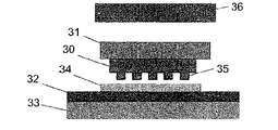
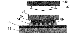
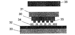
【解決手段】テンプレート30の転写すべきパターンの上に薄い金属層35が設けてあり、このテンプレート30を印写可能媒体34に接触させ、それとそれを保持するホルダ31を通してレーザ36のビーム37で照射する。このビーム37を金属層35が効率的に吸収し、この金属層からの熱を印写可能媒体34へ効率的に伝達するので、印写可能媒体34の加熱が迅速であり、熱が基板32に入って基板を歪めることがない。
【選択図】図4b
Description
31 テンプレートホルダ
32 基板
33 基板テーブル
34 印写可能媒体
35 熱吸収材料、金属
36 放射線源
37 放射線
Claims (25)
- 印写テンプレートおよび基板を保持するように構成した基板テーブルを含み、前記印写テンプレートがパターンを付けた表面、このパターンを付けた表面上に設けた熱吸収材料の層を有するリソグラフィ装置。
- 請求項1に記載の装置に於いて、前記熱吸収材料が金属である装置。
- 請求項2に記載の装置に於いて、前記金属がニッケル、クロムまたはアルミニウムを含む装置。
- 請求項1に記載の装置に於いて、前記熱吸収材料の層が厚さ10nm以上である装置。
- 請求項1に記載の装置に於いて、前記熱吸収材料の層が厚さ100nm以上である装置。
- 請求項1に記載の装置に於いて、前記熱吸収材料の層が厚さ1μm未満である装置。
- 請求項1に記載の装置に於いて、更に、前記熱吸収材料の層が吸収する波長の放射線を出すように構成した放射線源を含む装置。
- 請求項7に記載の装置に於いて、前記印写テンプレートは、前記熱吸収材料の層を除いて、前記放射線源が出す放射線の波長に透明である装置。
- 請求項7に記載の装置に於いて、前記印写テンプレートをテンプレートホルダで保持し、このテンプレートホルダは、前記放射線源が出す放射線の波長に透明である装置。
- 請求項7に記載の装置に於いて、前記熱吸収材料が金属である装置。
- 印写可能媒体に印写するように構成したパターンを備える表面を有する印写テンプレートであって、前記パターンの上に位置する熱吸収材料の層を含むテンプレート。
- 請求項11に記載のテンプレートに於いて、赤外、可視、または紫外放射線に透明である材料で作ってあるテンプレート。
- 請求項11に記載のテンプレートに於いて、前記熱吸収材料が金属であるテンプレート。
- 請求項13に記載のテンプレートに於いて、前記金属がニッケル、クロムまたはアルミニウムを含むテンプレート。
- 請求項11に記載のテンプレートに於いて、前記熱吸収材料の層が厚さ10nm以上である装置。テンプレート。
- 請求項11に記載のテンプレートに於いて、前記熱吸収材料の層が厚さ100nm以上であるテンプレート。
- 請求項11に記載のテンプレートに於いて、前記熱吸収材料の層が厚さ1μm未満であるテンプレート。
- 請求項11に記載のテンプレートに於いて、上記熱吸収材料の層が放射線を吸収するように構成してあるテンプレート。
- 請求項18に記載のテンプレートに於いて、前記熱吸収材料の層を除いて、前記放射線の波長に透明であるテンプレート。
- 請求項18に記載のテンプレートに於いて、前記熱吸収材料が金属であるテンプレート。
- 印写リソグラフィの方法であって、基板上の印写可能媒体の層の上に印写テンプレートを配置し、この印写テンプレートのパターンを付けた表面上に設けた熱吸収材料の層が印写可能媒体と接触するようにする工程、前記熱吸収材料の層を加熱しおよび熱を印写可能媒体へ伝達するように熱吸収材料の層を放射線で照射する工程、および前記印写テンプレートをこの印写可能媒体の中へ押込む工程を含む方法。
- 請求項21に記載の方法であって、更に、前記印写テンプレートを前記印写可能媒体の中へ押込んでから前記放射線を止める工程を含む方法。
- 請求項21に記載の方法であって、前記印写テンプレートを前記印写可能媒体に押付ける前に、前記熱吸収材料の層を前記放射線で照射する工程を含む方法。
- 請求項21に記載の方法であって、更に、前記熱吸収材料の層を前記放射線で照射する前に前記印写テンプレートを前記印写可能媒体に押付ける工程を含む方法。
- 請求項21に記載の方法に於いて、前記熱吸収材料が金属である方法。
Applications Claiming Priority (2)
| Application Number | Priority Date | Filing Date | Title |
|---|---|---|---|
| US11/189,010 US20070023976A1 (en) | 2005-07-26 | 2005-07-26 | Imprint lithography |
| US11/189,010 | 2005-07-26 |
Related Parent Applications (1)
| Application Number | Title | Priority Date | Filing Date |
|---|---|---|---|
| JP2006201431A Division JP5224660B2 (ja) | 2005-07-26 | 2006-07-25 | 印写リソグラフィの方法 |
Publications (2)
| Publication Number | Publication Date |
|---|---|
| JP2012131229A true JP2012131229A (ja) | 2012-07-12 |
| JP5458086B2 JP5458086B2 (ja) | 2014-04-02 |
Family
ID=37693460
Family Applications (2)
| Application Number | Title | Priority Date | Filing Date |
|---|---|---|---|
| JP2006201431A Expired - Fee Related JP5224660B2 (ja) | 2005-07-26 | 2006-07-25 | 印写リソグラフィの方法 |
| JP2011286258A Expired - Fee Related JP5458086B2 (ja) | 2005-07-26 | 2011-12-27 | 印写リソグラフィの方法 |
Family Applications Before (1)
| Application Number | Title | Priority Date | Filing Date |
|---|---|---|---|
| JP2006201431A Expired - Fee Related JP5224660B2 (ja) | 2005-07-26 | 2006-07-25 | 印写リソグラフィの方法 |
Country Status (2)
| Country | Link |
|---|---|
| US (1) | US20070023976A1 (ja) |
| JP (2) | JP5224660B2 (ja) |
Cited By (3)
| Publication number | Priority date | Publication date | Assignee | Title |
|---|---|---|---|---|
| JP2020511795A (ja) * | 2017-03-16 | 2020-04-16 | モレキュラー インプリンツ, インコーポレイテッドMolecular Imprints,Inc. | 光学ポリマーフィルムおよびそれを鋳造する方法 |
| US11320591B2 (en) | 2018-10-16 | 2022-05-03 | Magic Leap, Inc. | Methods and apparatuses for casting polymer products |
| US11318692B2 (en) | 2017-10-17 | 2022-05-03 | Magic Leap, Inc. | Methods and apparatuses for casting polymer products |
Families Citing this family (12)
| Publication number | Priority date | Publication date | Assignee | Title |
|---|---|---|---|---|
| US20070023976A1 (en) * | 2005-07-26 | 2007-02-01 | Asml Netherlands B.V. | Imprint lithography |
| JP2008192281A (ja) * | 2007-01-12 | 2008-08-21 | Ricoh Co Ltd | パターン及びその形成方法 |
| KR100843342B1 (ko) * | 2007-02-12 | 2008-07-03 | 삼성전자주식회사 | Uv 나노 임프린트 리소그래피 수행 공정 및 장치 |
| KR100874756B1 (ko) | 2007-10-18 | 2008-12-19 | 한국생산기술연구원 | 미세 임프린팅 장치 |
| US20090230594A1 (en) * | 2008-03-12 | 2009-09-17 | Hiroshi Deguchi | Imprint method and mold |
| JP5293169B2 (ja) * | 2008-03-12 | 2013-09-18 | 株式会社リコー | インプリント方法 |
| JP5107105B2 (ja) * | 2008-03-12 | 2012-12-26 | 株式会社リコー | インプリント方法 |
| KR100985060B1 (ko) | 2008-11-07 | 2010-10-04 | 한국과학기술원 | 패턴 전사 방법 및 패턴 전사 시스템 |
| US20100252961A1 (en) * | 2009-04-06 | 2010-10-07 | 3M Innovative Properties Company | Optical film replication on low thermal diffusivity tooling with conformal coating |
| DE102010043059A1 (de) * | 2009-11-06 | 2011-05-12 | Technische Universität Dresden | Imprinttemplate, Nanoimprintvorrichtung und Nanostrukturierungsverfahren |
| CN102543841B (zh) * | 2010-12-27 | 2014-07-30 | 中芯国际集成电路制造(上海)有限公司 | 半导体器件、形成栓塞的方法 |
| KR102698580B1 (ko) * | 2016-09-27 | 2024-08-23 | 일루미나, 인코포레이티드 | 임프린팅된 기판 |
Citations (5)
| Publication number | Priority date | Publication date | Assignee | Title |
|---|---|---|---|---|
| JP2003515461A (ja) * | 1999-11-30 | 2003-05-07 | スリーエム イノベイティブ プロパティズ カンパニー | マイクロ構造層の熱転写 |
| JP2003272998A (ja) * | 2002-03-14 | 2003-09-26 | Mitsubishi Electric Corp | 半導体装置の製造方法および半導体装置製造用モールド |
| JP2005111975A (ja) * | 2003-09-17 | 2005-04-28 | Dainippon Printing Co Ltd | 微細凹凸パターンの形成方法 |
| JP2005515098A (ja) * | 2002-01-25 | 2005-05-26 | ライスター プロセス テクノロジーズ | 微小構造物の成形方法 |
| JP5224660B2 (ja) * | 2005-07-26 | 2013-07-03 | エーエスエムエル ネザーランズ ビー.ブイ. | 印写リソグラフィの方法 |
Family Cites Families (68)
| Publication number | Priority date | Publication date | Assignee | Title |
|---|---|---|---|---|
| FR2402526A1 (fr) * | 1977-09-09 | 1979-04-06 | Isobox Barbier Sa | Dispositif et procede de moulage de matieres plastiques expansees, par rayonnement ultra-haute frequence |
| US4262875A (en) * | 1979-08-17 | 1981-04-21 | Rca Corporation | Information record stampers |
| US4747864A (en) * | 1986-06-19 | 1988-05-31 | Corning Glass Works | Process for the precision molding of glass articles |
| US5002476A (en) * | 1989-11-24 | 1991-03-26 | Lockheed Corporation | Tooling for composite parts |
| EP0488239B1 (en) * | 1990-11-28 | 1997-07-30 | Sharp Kabushiki Kaisha | Method for manufacturing a stamper |
| JP3006199B2 (ja) * | 1991-09-03 | 2000-02-07 | 株式会社日立製作所 | 光ディスクの製造方法 |
| JPH06119661A (ja) * | 1992-10-05 | 1994-04-28 | Sharp Corp | スタンパー及びスタンパーの製造方法 |
| US5388803A (en) * | 1993-08-17 | 1995-02-14 | General Electric Company | Apparatus for producing textured articles |
| US5512131A (en) * | 1993-10-04 | 1996-04-30 | President And Fellows Of Harvard College | Formation of microstamped patterns on surfaces and derivative articles |
| US5512219A (en) * | 1994-06-03 | 1996-04-30 | Reflexite Corporation | Method of casting a microstructure sheet having an array of prism elements using a reusable polycarbonate mold |
| US20040036201A1 (en) * | 2000-07-18 | 2004-02-26 | Princeton University | Methods and apparatus of field-induced pressure imprint lithography |
| US6518189B1 (en) * | 1995-11-15 | 2003-02-11 | Regents Of The University Of Minnesota | Method and apparatus for high density nanostructures |
| US6482742B1 (en) * | 2000-07-18 | 2002-11-19 | Stephen Y. Chou | Fluid pressure imprint lithography |
| US5772905A (en) * | 1995-11-15 | 1998-06-30 | Regents Of The University Of Minnesota | Nanoimprint lithography |
| US6309580B1 (en) * | 1995-11-15 | 2001-10-30 | Regents Of The University Of Minnesota | Release surfaces, particularly for use in nanoimprint lithography |
| US5824094A (en) * | 1997-10-17 | 1998-10-20 | Acromed Corporation | Spinal disc |
| EP1358987A3 (en) * | 1998-10-14 | 2004-03-03 | Gyros AB | A replication matrix |
| EP1003078A3 (en) * | 1998-11-17 | 2001-11-07 | Corning Incorporated | Replicating a nanoscale pattern |
| US6334960B1 (en) * | 1999-03-11 | 2002-01-01 | Board Of Regents, The University Of Texas System | Step and flash imprint lithography |
| SE515607C2 (sv) * | 1999-12-10 | 2001-09-10 | Obducat Ab | Anordning och metod vid tillverkning av strukturer |
| US6165911A (en) * | 1999-12-29 | 2000-12-26 | Calveley; Peter Braden | Method of patterning a metal layer |
| ATE332517T1 (de) * | 2000-01-21 | 2006-07-15 | Obducat Ab | Form zur nanobedruckung |
| SE515785C2 (sv) * | 2000-02-23 | 2001-10-08 | Obducat Ab | Anordning för homogen värmning av ett objekt och användning av anordningen |
| SE515962C2 (sv) * | 2000-03-15 | 2001-11-05 | Obducat Ab | Anordning för överföring av mönster till objekt |
| SE516194C2 (sv) * | 2000-04-18 | 2001-12-03 | Obducat Ab | Substrat för samt process vid tillverkning av strukturer |
| US6365059B1 (en) * | 2000-04-28 | 2002-04-02 | Alexander Pechenik | Method for making a nano-stamp and for forming, with the stamp, nano-size elements on a substrate |
| SE516414C2 (sv) * | 2000-05-24 | 2002-01-15 | Obducat Ab | Metod vid tillverkning av en mall, samt mallen tillverkad därav |
| SG142150A1 (en) * | 2000-07-16 | 2008-05-28 | Univ Texas | High-resolution overlay alignment systems for imprint lithography |
| KR100827741B1 (ko) * | 2000-07-17 | 2008-05-07 | 보드 오브 리전츠, 더 유니버시티 오브 텍사스 시스템 | 임프린트 리소그래피 공정을 위한 자동 유체 분배 방법 및시스템 |
| US7211214B2 (en) * | 2000-07-18 | 2007-05-01 | Princeton University | Laser assisted direct imprint lithography |
| JP2004505273A (ja) * | 2000-08-01 | 2004-02-19 | ボード・オブ・リージエンツ,ザ・ユニバーシテイ・オブ・テキサス・システム | 転写リソグラフィのための透明テンプレートと基板の間のギャップおよび配向を高精度でセンシングするための方法 |
| SE519478C2 (sv) * | 2000-09-19 | 2003-03-04 | Obducat Ab | Etsförfarande, såväl som ramelement, mask och förtillverkat substratelement för användning i sådan etsning |
| CN100365507C (zh) * | 2000-10-12 | 2008-01-30 | 德克萨斯州大学系统董事会 | 用于室温下低压微刻痕和毫微刻痕光刻的模板 |
| US6875379B2 (en) * | 2000-12-29 | 2005-04-05 | Amkor Technology, Inc. | Tool and method for forming an integrated optical circuit |
| US6964793B2 (en) * | 2002-05-16 | 2005-11-15 | Board Of Regents, The University Of Texas System | Method for fabricating nanoscale patterns in light curable compositions using an electric field |
| US6847433B2 (en) * | 2001-06-01 | 2005-01-25 | Agere Systems, Inc. | Holder, system, and process for improving overlay in lithography |
| SE519573C2 (sv) * | 2001-07-05 | 2003-03-11 | Obducat Ab | Stamp med antividhäftningsskikt samt sätt att framställa och sätt att reparera en sådan stamp |
| US6821460B2 (en) * | 2001-07-16 | 2004-11-23 | Imation Corp. | Two-sided replication of data storage media |
| JP2003067984A (ja) * | 2001-08-24 | 2003-03-07 | Toshiba Corp | 光ディスク製造方法とこれにより製造される光ディスク |
| US20030071016A1 (en) * | 2001-10-11 | 2003-04-17 | Wu-Sheng Shih | Patterned structure reproduction using nonsticking mold |
| US20030080472A1 (en) * | 2001-10-29 | 2003-05-01 | Chou Stephen Y. | Lithographic method with bonded release layer for molding small patterns |
| JP3690740B2 (ja) * | 2001-11-15 | 2005-08-31 | 敏夫 川井 | 光ディスク用のスタンパー |
| US7144539B2 (en) * | 2002-04-04 | 2006-12-05 | Obducat Ab | Imprint method and device |
| US6849558B2 (en) * | 2002-05-22 | 2005-02-01 | The Board Of Trustees Of The Leland Stanford Junior University | Replication and transfer of microstructures and nanostructures |
| US7252492B2 (en) * | 2002-06-20 | 2007-08-07 | Obducat Ab | Devices and methods for aligning a stamp and a substrate |
| US6932934B2 (en) * | 2002-07-11 | 2005-08-23 | Molecular Imprints, Inc. | Formation of discontinuous films during an imprint lithography process |
| US7077992B2 (en) * | 2002-07-11 | 2006-07-18 | Molecular Imprints, Inc. | Step and repeat imprint lithography processes |
| US6908861B2 (en) * | 2002-07-11 | 2005-06-21 | Molecular Imprints, Inc. | Method for imprint lithography using an electric field |
| US7027156B2 (en) * | 2002-08-01 | 2006-04-11 | Molecular Imprints, Inc. | Scatterometry alignment for imprint lithography |
| WO2004020176A1 (de) * | 2002-08-09 | 2004-03-11 | Leonhard Kurz Gmbh & Co. Kg | Laserunterstütztes replizierverfahren |
| US6755984B2 (en) * | 2002-10-24 | 2004-06-29 | Hewlett-Packard Development Company, L.P. | Micro-casted silicon carbide nano-imprinting stamp |
| US6916511B2 (en) * | 2002-10-24 | 2005-07-12 | Hewlett-Packard Development Company, L.P. | Method of hardening a nano-imprinting stamp |
| JP2005005245A (ja) * | 2002-11-08 | 2005-01-06 | Fuji Photo Film Co Ltd | 転写素材の転写方法、形状転写方法及び転写装置 |
| EP1443344A1 (en) * | 2003-01-29 | 2004-08-04 | Heptagon Oy | Manufacturing micro-structured elements |
| WO2004086471A1 (en) * | 2003-03-27 | 2004-10-07 | Korea Institute Of Machinery & Materials | Uv nanoimprint lithography process using elementwise embossed stamp and selectively additive pressurization |
| US20040209123A1 (en) * | 2003-04-17 | 2004-10-21 | Bajorek Christopher H. | Method of fabricating a discrete track recording disk using a bilayer resist for metal lift-off |
| TW568349U (en) * | 2003-05-02 | 2003-12-21 | Ind Tech Res Inst | Parallelism adjusting device for nano-transferring |
| TW570290U (en) * | 2003-05-02 | 2004-01-01 | Ind Tech Res Inst | Uniform pressing device for nanometer transfer-print |
| TWI253975B (en) * | 2003-05-13 | 2006-05-01 | Kuraray Co | Mold for molding resins and process for producing the same |
| US7245406B2 (en) * | 2003-09-17 | 2007-07-17 | Dai Nippon Printing Co., Ltd. | Method for forming fine concavo-convex patterns, method for producing optical diffraction structure, and method for copying optical diffraction structure |
| JP2005101201A (ja) * | 2003-09-24 | 2005-04-14 | Canon Inc | ナノインプリント装置 |
| JP3889386B2 (ja) * | 2003-09-30 | 2007-03-07 | 株式会社東芝 | インプリント装置及びインプリント方法 |
| US20050156353A1 (en) * | 2004-01-15 | 2005-07-21 | Watts Michael P. | Method to improve the flow rate of imprinting material |
| KR100558754B1 (ko) * | 2004-02-24 | 2006-03-10 | 한국기계연구원 | Uv 나노임프린트 리소그래피 공정 및 이 공정을수행하는 장치 |
| TWI243796B (en) * | 2004-06-08 | 2005-11-21 | Ind Tech Res Inst | Device of nano-structure imprint for pattern transfer and method of the same |
| US7119314B2 (en) * | 2004-06-30 | 2006-10-10 | Intel Corporation | Radio frequency and microwave radiation used in conjunction with convective thermal heating to expedite curing of an imprinted material |
| JP4109234B2 (ja) * | 2004-09-24 | 2008-07-02 | 株式会社日本製鋼所 | 微細転写方法および装置 |
| JP2006168034A (ja) * | 2004-12-14 | 2006-06-29 | Ricoh Co Ltd | プレス成形方法及び熱可塑性樹脂成形体 |
-
2005
- 2005-07-26 US US11/189,010 patent/US20070023976A1/en not_active Abandoned
-
2006
- 2006-07-25 JP JP2006201431A patent/JP5224660B2/ja not_active Expired - Fee Related
-
2011
- 2011-12-27 JP JP2011286258A patent/JP5458086B2/ja not_active Expired - Fee Related
Patent Citations (5)
| Publication number | Priority date | Publication date | Assignee | Title |
|---|---|---|---|---|
| JP2003515461A (ja) * | 1999-11-30 | 2003-05-07 | スリーエム イノベイティブ プロパティズ カンパニー | マイクロ構造層の熱転写 |
| JP2005515098A (ja) * | 2002-01-25 | 2005-05-26 | ライスター プロセス テクノロジーズ | 微小構造物の成形方法 |
| JP2003272998A (ja) * | 2002-03-14 | 2003-09-26 | Mitsubishi Electric Corp | 半導体装置の製造方法および半導体装置製造用モールド |
| JP2005111975A (ja) * | 2003-09-17 | 2005-04-28 | Dainippon Printing Co Ltd | 微細凹凸パターンの形成方法 |
| JP5224660B2 (ja) * | 2005-07-26 | 2013-07-03 | エーエスエムエル ネザーランズ ビー.ブイ. | 印写リソグラフィの方法 |
Cited By (7)
| Publication number | Priority date | Publication date | Assignee | Title |
|---|---|---|---|---|
| JP2020511795A (ja) * | 2017-03-16 | 2020-04-16 | モレキュラー インプリンツ, インコーポレイテッドMolecular Imprints,Inc. | 光学ポリマーフィルムおよびそれを鋳造する方法 |
| US11298856B2 (en) | 2017-03-16 | 2022-04-12 | Molecular Imprints, Inc. | Optical polymer films and methods for casting the same |
| JP7149284B2 (ja) | 2017-03-16 | 2022-10-06 | モレキュラー インプリンツ, インコーポレイテッド | 光学ポリマーフィルムおよびそれを鋳造する方法 |
| US11318692B2 (en) | 2017-10-17 | 2022-05-03 | Magic Leap, Inc. | Methods and apparatuses for casting polymer products |
| US11787138B2 (en) | 2017-10-17 | 2023-10-17 | Magic Leap, Inc. | Methods and apparatuses for casting polymer products |
| US12030269B2 (en) | 2017-10-17 | 2024-07-09 | Magic Leap, Inc. | Methods and apparatuses for casting polymer products |
| US11320591B2 (en) | 2018-10-16 | 2022-05-03 | Magic Leap, Inc. | Methods and apparatuses for casting polymer products |
Also Published As
| Publication number | Publication date |
|---|---|
| JP5224660B2 (ja) | 2013-07-03 |
| JP5458086B2 (ja) | 2014-04-02 |
| US20070023976A1 (en) | 2007-02-01 |
| JP2007036246A (ja) | 2007-02-08 |
Similar Documents
| Publication | Publication Date | Title |
|---|---|---|
| JP5458086B2 (ja) | 印写リソグラフィの方法 | |
| JP5883527B2 (ja) | インプリント・リソグラフィ | |
| US7363854B2 (en) | System and method for patterning both sides of a substrate utilizing imprint lithography | |
| JP4625042B2 (ja) | インプリントリソグラフィ | |
| TWI387856B (zh) | 壓印微影術 | |
| JP4526512B2 (ja) | インプリント・リソグラフィ | |
| US7354698B2 (en) | Imprint lithography | |
| JP4398423B2 (ja) | インプリント・リソグラフィ | |
| JP4398422B2 (ja) | インプリント・リソグラフィ |
Legal Events
| Date | Code | Title | Description |
|---|---|---|---|
| A977 | Report on retrieval |
Free format text: JAPANESE INTERMEDIATE CODE: A971007 Effective date: 20130913 |
|
| A131 | Notification of reasons for refusal |
Free format text: JAPANESE INTERMEDIATE CODE: A132 Effective date: 20130919 |
|
| A521 | Request for written amendment filed |
Free format text: JAPANESE INTERMEDIATE CODE: A523 Effective date: 20131206 |
|
| TRDD | Decision of grant or rejection written | ||
| A01 | Written decision to grant a patent or to grant a registration (utility model) |
Free format text: JAPANESE INTERMEDIATE CODE: A01 Effective date: 20131225 |
|
| A61 | First payment of annual fees (during grant procedure) |
Free format text: JAPANESE INTERMEDIATE CODE: A61 Effective date: 20140110 |
|
| R150 | Certificate of patent or registration of utility model |
Ref document number: 5458086 Country of ref document: JP Free format text: JAPANESE INTERMEDIATE CODE: R150 Free format text: JAPANESE INTERMEDIATE CODE: R150 |
|
| R250 | Receipt of annual fees |
Free format text: JAPANESE INTERMEDIATE CODE: R250 |
|
| R250 | Receipt of annual fees |
Free format text: JAPANESE INTERMEDIATE CODE: R250 |
|
| R250 | Receipt of annual fees |
Free format text: JAPANESE INTERMEDIATE CODE: R250 |
|
| R250 | Receipt of annual fees |
Free format text: JAPANESE INTERMEDIATE CODE: R250 |
|
| R250 | Receipt of annual fees |
Free format text: JAPANESE INTERMEDIATE CODE: R250 |
|
| R250 | Receipt of annual fees |
Free format text: JAPANESE INTERMEDIATE CODE: R250 |
|
| LAPS | Cancellation because of no payment of annual fees |