JP2012156718A - 出力回路、温度スイッチic、及び、電池パック - Google Patents
出力回路、温度スイッチic、及び、電池パック Download PDFInfo
- Publication number
- JP2012156718A JP2012156718A JP2011013326A JP2011013326A JP2012156718A JP 2012156718 A JP2012156718 A JP 2012156718A JP 2011013326 A JP2011013326 A JP 2011013326A JP 2011013326 A JP2011013326 A JP 2011013326A JP 2012156718 A JP2012156718 A JP 2012156718A
- Authority
- JP
- Japan
- Prior art keywords
- output
- voltage
- circuit
- power supply
- terminal
- Prior art date
- Legal status (The legal status is an assumption and is not a legal conclusion. Google has not performed a legal analysis and makes no representation as to the accuracy of the status listed.)
- Granted
Links
Images




Classifications
-
- H—ELECTRICITY
- H03—ELECTRONIC CIRCUITRY
- H03K—PULSE TECHNIQUE
- H03K17/00—Electronic switching or gating, i.e. not by contact-making and –breaking
- H03K17/20—Modifications for resetting core switching units to a predetermined state
-
- A—HUMAN NECESSITIES
- A63—SPORTS; GAMES; AMUSEMENTS
- A63B—APPARATUS FOR PHYSICAL TRAINING, GYMNASTICS, SWIMMING, CLIMBING, OR FENCING; BALL GAMES; TRAINING EQUIPMENT
- A63B67/00—Sporting games or accessories therefor, not provided for in groups A63B1/00 - A63B65/00
- A63B67/04—Table games physically beneficial for the human body, modelled on outdoor sports, e.g. table tennis
- A63B67/045—Supports for table tennis nets
-
- A—HUMAN NECESSITIES
- A63—SPORTS; GAMES; AMUSEMENTS
- A63B—APPARATUS FOR PHYSICAL TRAINING, GYMNASTICS, SWIMMING, CLIMBING, OR FENCING; BALL GAMES; TRAINING EQUIPMENT
- A63B71/00—Games or sports accessories not covered in groups A63B1/00 - A63B69/00
- A63B71/04—Games or sports accessories not covered in groups A63B1/00 - A63B69/00 for small-room or indoor sporting games
-
- H—ELECTRICITY
- H02—GENERATION; CONVERSION OR DISTRIBUTION OF ELECTRIC POWER
- H02J—ELECTRIC POWER NETWORKS; CIRCUIT ARRANGEMENTS OR SYSTEMS FOR SUPPLYING OR DISTRIBUTING ELECTRIC POWER; SYSTEMS FOR STORING ELECTRIC ENERGY
- H02J7/00—Circuit arrangements for charging or discharging batteries or for supplying loads from batteries
- H02J7/02—Circuit arrangements for charging or discharging batteries or for supplying loads from batteries for charging batteries from AC mains by converters
- H02J7/04—Regulation of charging current or voltage
-
- H—ELECTRICITY
- H02—GENERATION; CONVERSION OR DISTRIBUTION OF ELECTRIC POWER
- H02J—ELECTRIC POWER NETWORKS; CIRCUIT ARRANGEMENTS OR SYSTEMS FOR SUPPLYING OR DISTRIBUTING ELECTRIC POWER; SYSTEMS FOR STORING ELECTRIC ENERGY
- H02J7/00—Circuit arrangements for charging or discharging batteries or for supplying loads from batteries
- H02J7/60—Circuit arrangements for charging or discharging batteries or for supplying loads from batteries including safety or protection arrangements
- H02J7/663—Circuit arrangements for charging or discharging batteries or for supplying loads from batteries including safety or protection arrangements using battery or load disconnect circuits
-
- H—ELECTRICITY
- H02—GENERATION; CONVERSION OR DISTRIBUTION OF ELECTRIC POWER
- H02J—ELECTRIC POWER NETWORKS; CIRCUIT ARRANGEMENTS OR SYSTEMS FOR SUPPLYING OR DISTRIBUTING ELECTRIC POWER; SYSTEMS FOR STORING ELECTRIC ENERGY
- H02J7/00—Circuit arrangements for charging or discharging batteries or for supplying loads from batteries
- H02J7/90—Regulation of charging or discharging current or voltage
- H02J7/971—Regulation of charging or discharging current or voltage the charge cycle being controlled or terminated in response to non-electric parameters
- H02J7/975—Regulation of charging or discharging current or voltage the charge cycle being controlled or terminated in response to non-electric parameters in response to temperature
- H02J7/977—Regulation of charging or discharging current or voltage the charge cycle being controlled or terminated in response to non-electric parameters in response to temperature of the battery
-
- A—HUMAN NECESSITIES
- A63—SPORTS; GAMES; AMUSEMENTS
- A63B—APPARATUS FOR PHYSICAL TRAINING, GYMNASTICS, SWIMMING, CLIMBING, OR FENCING; BALL GAMES; TRAINING EQUIPMENT
- A63B2208/00—Characteristics or parameters related to the user or player
- A63B2208/12—Characteristics or parameters related to the user or player specially adapted for children
-
- H—ELECTRICITY
- H03—ELECTRONIC CIRCUITRY
- H03K—PULSE TECHNIQUE
- H03K19/00—Logic circuits, i.e. having at least two inputs acting on one output; Inverting circuits
- H03K19/0008—Arrangements for reducing power consumption
- H03K19/0013—Arrangements for reducing power consumption in field effect transistor circuits
-
- H—ELECTRICITY
- H03—ELECTRONIC CIRCUITRY
- H03K—PULSE TECHNIQUE
- H03K19/00—Logic circuits, i.e. having at least two inputs acting on one output; Inverting circuits
- H03K19/003—Modifications for increasing the reliability for protection
- H03K19/00346—Modifications for eliminating interference or parasitic voltages or currents
- H03K19/00361—Modifications for eliminating interference or parasitic voltages or currents in field effect transistor circuits
-
- H—ELECTRICITY
- H03—ELECTRONIC CIRCUITRY
- H03K—PULSE TECHNIQUE
- H03K19/00—Logic circuits, i.e. having at least two inputs acting on one output; Inverting circuits
- H03K19/0175—Coupling arrangements; Interface arrangements
- H03K19/0185—Coupling arrangements; Interface arrangements using field effect transistors only
- H03K19/018507—Interface arrangements
- H03K19/018521—Interface arrangements of complementary type, e.g. CMOS
Landscapes
- Engineering & Computer Science (AREA)
- Power Engineering (AREA)
- Health & Medical Sciences (AREA)
- General Health & Medical Sciences (AREA)
- Physical Education & Sports Medicine (AREA)
- Charge And Discharge Circuits For Batteries Or The Like (AREA)
- Protection Of Static Devices (AREA)
- Secondary Cells (AREA)
- Battery Mounting, Suspending (AREA)
- Logic Circuits (AREA)
Abstract
【解決手段】インバータ回路の電源端子にスイッチ回路を設け、電源電圧が回路の動作電圧以下のとき、スイッチ回路がインバータ回路の動作を停止させる。そして、インバータ回路の出力端子に電流源を設け、インバータ回路の動作が停止したときに出力を電源電圧に固定する、ように構成した。
【選択図】図1
Description
従来の出力回路は、入力端子に接続されたインバータ97と、出力ドライバであるNMOSトランジスタ93と、電源と接地の間に設けられたダイオード接続されたNMOSトランジスタ95及び容量96と、それらによって制御されるNMOSトランジスタ94と、を備える。
従来の出力回路は、NMOSトランジスタ94はサイズが大きいので、出力回路の面積が大きくなってしまう、という課題があった。
図1は、本実施形態の出力回路を示す回路図である。
出力回路10は、PMOSトランジスタ11及び12と、NMOSトランジスタ21及び22と、電流源31を備える。
電源が投入され、電源電圧VDDが高くなる。この時、電源電圧VDDがPMOSトランジスタ12の閾値電圧の絶対値|Vthp12|よりも低いと、PMOSトランジスタ12はオフする。すると、電源電圧VDDは、インバータ36に供給されない。よって、このインバータ36の出力端子が電流源31によってプルダウンされるので、インバータ36の出力電圧は接地電圧VSSである。出力ドライバであるNMOSトランジスタ22は、ゲート電圧が接地電圧VSSになるのでオフし、出力回路10の出力端子はハイインピーダンス状態になる。従って、出力回路10の出力端子は、それを入力端子に接続する後段の回路の電源電圧にプルアップされるので、後段の回路は誤動作しない。
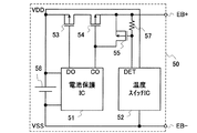
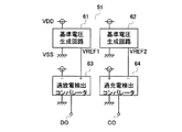
[電池58が過充電状態である時の動作]電池パック50に充電器(図示せず)が接続される。基準電圧生成回路62は、電池58が過充電状態であることを示す過充電電圧に対応した基準電圧VREF2を生成する。過充電検出コンパレータ64は、電池58の電圧の分圧電圧と基準電圧VREF2とを比較し、比較結果により、出力電圧を反転させる。具体的には、電池58の電圧の分圧電圧が基準電圧VREF2以上になると、過充電検出コンパレータ64の出力電圧は反転してハイレベルになる。すると、P型FET54はオフし、電池58への充電が停止する。
また、抵抗57やP型FET55などは、温度スイッチIC52によって内蔵されても良い。
31 電流源
50 電池パック
51 電池保護IC
52 温度スイッチIC
58 電池
61、62、71、72 基準電圧生成回路
63 過放電検出コンパレータ
64 過充電検出コンパレータ
73 高温検出コンパレータ
74 低温検出コンパレータ
75 温度電圧生成回路
Claims (5)
- オープンドレイン出力の出力回路であって、
前記出力回路の入力端子に接続されたインバータ回路と、
ゲートが前記インバータ回路の出力端子に接続され、ドレインが前記出力回路の出力端子に接続され、ソースが第1電源端子に接続された出力MOSトランジスタと、
前記インバータ回路と第2電源端子の間に設けられたスイッチ回路と、
前記出力MOSトランジスタのゲートと前記第1電源端子との間に設けられた電流源と、 を備え、
前記スイッチ回路は、電源電圧が前記出力回路の最低動作電圧よりも低いとオフすることを特徴とする出力回路。 - 前記スイッチ回路は、ゲートが第1電源端子に接続されたMOSトランジスタで構成され、
前記MOSトランジスタの閾値電圧の絶対値は前記最低動作電圧である、ことを特徴とする請求項1記載の出力回路。 - 前記スイッチ回路は、更に第1電源端子と第2電源端子の間に直列に接続さした第2の電流源と第2のMOSトランジスタとを備え、
前記第2の電流源と前記第2のMOSトランジスタとの接続ノードが前記MOSトランジスタのゲートに接続され、前記MOSトランジスタと前記第2のMOSトランジスタの閾値電圧の絶対値の合計電圧が前記最低動作電圧である、ことを特徴とする請求項2記載の出力回路。 - 温度に基づいた温度電圧を生成する温度電圧生成回路と、
異常温度に対応した基準電圧を生成する基準電圧生成回路と、
前記温度電圧と前記基準電圧とを比較し、比較結果により、出力電圧を反転させるコンパレータと、
前記コンパレータの出力端子に接続される、請求項1から3のいずれか記載の出力回路と、を備えることを特徴とする温度スイッチIC。 - 電池と前記電池の充放電を制御する電池保護ICを備えた電池パックであって、
前記電池の充放電経路に設けられる充電制御用FETと、
異常温度を検出する請求項4記載の温度スイッチICと、を備え
前記温度スイッチICが異常温度を検出すると、前記充電制御用FETをオフすることを特徴とする電池パック。
Priority Applications (5)
| Application Number | Priority Date | Filing Date | Title |
|---|---|---|---|
| JP2011013326A JP5588370B2 (ja) | 2011-01-25 | 2011-01-25 | 出力回路、温度スイッチic、及び、電池パック |
| TW101100929A TWI539747B (zh) | 2011-01-25 | 2012-01-10 | Output circuit, temperature switch IC and battery pack |
| CN201210015595.9A CN102624371B (zh) | 2011-01-25 | 2012-01-18 | 输出电路、温度开关ic以及电池组 |
| KR1020120006176A KR101751547B1 (ko) | 2011-01-25 | 2012-01-19 | 출력 회로, 온도 스위치 ic, 및 전지 팩 |
| US13/355,740 US9118326B2 (en) | 2011-01-25 | 2012-01-23 | Output circuit, temperature switch IC, and battery pack |
Applications Claiming Priority (1)
| Application Number | Priority Date | Filing Date | Title |
|---|---|---|---|
| JP2011013326A JP5588370B2 (ja) | 2011-01-25 | 2011-01-25 | 出力回路、温度スイッチic、及び、電池パック |
Publications (2)
| Publication Number | Publication Date |
|---|---|
| JP2012156718A true JP2012156718A (ja) | 2012-08-16 |
| JP5588370B2 JP5588370B2 (ja) | 2014-09-10 |
Family
ID=46543705
Family Applications (1)
| Application Number | Title | Priority Date | Filing Date |
|---|---|---|---|
| JP2011013326A Expired - Fee Related JP5588370B2 (ja) | 2011-01-25 | 2011-01-25 | 出力回路、温度スイッチic、及び、電池パック |
Country Status (5)
| Country | Link |
|---|---|
| US (1) | US9118326B2 (ja) |
| JP (1) | JP5588370B2 (ja) |
| KR (1) | KR101751547B1 (ja) |
| CN (1) | CN102624371B (ja) |
| TW (1) | TWI539747B (ja) |
Families Citing this family (7)
| Publication number | Priority date | Publication date | Assignee | Title |
|---|---|---|---|---|
| WO2014024337A1 (ja) * | 2012-08-10 | 2014-02-13 | パナソニック株式会社 | バッテリー装置およびバッテリー制御装置 |
| JP6719233B2 (ja) * | 2016-03-07 | 2020-07-08 | エイブリック株式会社 | 出力回路 |
| TWI583089B (zh) * | 2016-04-29 | 2017-05-11 | 盧昭正 | 電池放電保護裝置 |
| KR101944989B1 (ko) * | 2017-06-20 | 2019-02-01 | 장철호 | 장애인 및 비장애인용 비상 경고 장치 |
| DE102020104129A1 (de) * | 2019-05-03 | 2020-11-05 | Taiwan Semiconductor Manufacturing Co., Ltd. | Logikpufferschaltung und verfahren |
| US10979049B2 (en) * | 2019-05-03 | 2021-04-13 | Taiwan Semiconductor Manufacturing Company Ltd. | Logic buffer circuit and method |
| CN115800424B (zh) * | 2022-09-28 | 2025-03-21 | 深圳市创芯微微电子有限公司 | 一种正端充放电的电池保护芯片及系统 |
Citations (8)
| Publication number | Priority date | Publication date | Assignee | Title |
|---|---|---|---|---|
| JPS5323669A (en) * | 1976-08-17 | 1978-03-04 | Citizen Watch Co Ltd | Small electronic device |
| JPS592436A (ja) * | 1982-06-29 | 1984-01-09 | Fujitsu Ltd | Ttl回路 |
| US4912346A (en) * | 1988-07-18 | 1990-03-27 | Mitsubishi Denki Kabushiki Kaisha | Input/output circuit for IC card |
| JPH02210913A (ja) * | 1989-02-10 | 1990-08-22 | Matsushita Electric Ind Co Ltd | Mos集積回路 |
| JPH11201830A (ja) * | 1997-11-17 | 1999-07-30 | Fuji Electric Co Ltd | 温度検出機能内蔵ドライバic |
| JP2005260868A (ja) * | 2004-03-15 | 2005-09-22 | Nec Saitama Ltd | 移動通信機器 |
| JP2006112889A (ja) * | 2004-10-14 | 2006-04-27 | Kawasaki Microelectronics Kk | 電源電圧検出回路 |
| JP2009198476A (ja) * | 2008-01-24 | 2009-09-03 | Ricoh Co Ltd | 電圧検出回路 |
Family Cites Families (16)
| Publication number | Priority date | Publication date | Assignee | Title |
|---|---|---|---|---|
| JPS5750135A (en) * | 1980-09-09 | 1982-03-24 | Nec Corp | Inverter circuit |
| JPS5869115A (ja) * | 1981-10-20 | 1983-04-25 | Toshiba Corp | 半導体集積回路 |
| US4791323A (en) * | 1986-10-23 | 1988-12-13 | Silicon Systems, Inc. | Level translation circuit |
| JPH0334719A (ja) * | 1989-06-30 | 1991-02-14 | Toshiba Micro Electron Kk | 半導体集積回路 |
| JPH0675668A (ja) | 1992-08-25 | 1994-03-18 | Nec Corp | 出力回路 |
| US5406139A (en) * | 1993-03-19 | 1995-04-11 | Advanced Micro Devices, Inc. | Input buffer utilizing a cascode to provide a zero power TTL to CMOS input with high speed switching |
| US6069491A (en) * | 1997-02-17 | 2000-05-30 | Siemens Aktiengesellschaft | Integrated buffer circuit |
| US6362665B1 (en) * | 1999-11-19 | 2002-03-26 | Intersil Americas Inc. | Backwards drivable MOS output driver |
| US6362655B1 (en) * | 2000-11-15 | 2002-03-26 | Intel Corporation | Linear active resistor and driver circuit incorporating the same |
| US7598779B1 (en) * | 2004-10-08 | 2009-10-06 | Altera Corporation | Dual-mode LVDS/CML transmitter methods and apparatus |
| US8018268B1 (en) * | 2004-11-19 | 2011-09-13 | Cypress Semiconductor Corporation | Over-voltage tolerant input circuit |
| JP4764234B2 (ja) * | 2006-04-07 | 2011-08-31 | 株式会社東芝 | インピーダンス変換回路及び電子機器 |
| JP2008028442A (ja) * | 2006-07-18 | 2008-02-07 | Ricoh Co Ltd | 電流駆動型差動ドライバを備える半導体装置及び電流駆動差動ドライバの動作制御方法 |
| US7511534B1 (en) * | 2007-10-05 | 2009-03-31 | Micron Technology, Inc. | Circuits, devices, systems, and methods of operation for a linear output driver |
| JP5468882B2 (ja) * | 2009-07-03 | 2014-04-09 | セイコーインスツル株式会社 | Cmos入力バッファ回路 |
| JP5442558B2 (ja) * | 2010-08-06 | 2014-03-12 | ルネサスエレクトロニクス株式会社 | 出力回路及びデータドライバ及び表示装置 |
-
2011
- 2011-01-25 JP JP2011013326A patent/JP5588370B2/ja not_active Expired - Fee Related
-
2012
- 2012-01-10 TW TW101100929A patent/TWI539747B/zh not_active IP Right Cessation
- 2012-01-18 CN CN201210015595.9A patent/CN102624371B/zh not_active Expired - Fee Related
- 2012-01-19 KR KR1020120006176A patent/KR101751547B1/ko not_active Expired - Fee Related
- 2012-01-23 US US13/355,740 patent/US9118326B2/en not_active Expired - Fee Related
Patent Citations (8)
| Publication number | Priority date | Publication date | Assignee | Title |
|---|---|---|---|---|
| JPS5323669A (en) * | 1976-08-17 | 1978-03-04 | Citizen Watch Co Ltd | Small electronic device |
| JPS592436A (ja) * | 1982-06-29 | 1984-01-09 | Fujitsu Ltd | Ttl回路 |
| US4912346A (en) * | 1988-07-18 | 1990-03-27 | Mitsubishi Denki Kabushiki Kaisha | Input/output circuit for IC card |
| JPH02210913A (ja) * | 1989-02-10 | 1990-08-22 | Matsushita Electric Ind Co Ltd | Mos集積回路 |
| JPH11201830A (ja) * | 1997-11-17 | 1999-07-30 | Fuji Electric Co Ltd | 温度検出機能内蔵ドライバic |
| JP2005260868A (ja) * | 2004-03-15 | 2005-09-22 | Nec Saitama Ltd | 移動通信機器 |
| JP2006112889A (ja) * | 2004-10-14 | 2006-04-27 | Kawasaki Microelectronics Kk | 電源電圧検出回路 |
| JP2009198476A (ja) * | 2008-01-24 | 2009-09-03 | Ricoh Co Ltd | 電圧検出回路 |
Also Published As
| Publication number | Publication date |
|---|---|
| TW201304413A (zh) | 2013-01-16 |
| KR101751547B1 (ko) | 2017-06-27 |
| CN102624371A (zh) | 2012-08-01 |
| JP5588370B2 (ja) | 2014-09-10 |
| US20120187911A1 (en) | 2012-07-26 |
| CN102624371B (zh) | 2016-06-22 |
| TWI539747B (zh) | 2016-06-21 |
| KR20120086256A (ko) | 2012-08-02 |
| US9118326B2 (en) | 2015-08-25 |
Similar Documents
| Publication | Publication Date | Title |
|---|---|---|
| US11646569B2 (en) | Secondary battery protection circuit, secondary battery protection apparatus and battery pack | |
| JP5457206B2 (ja) | 電池パック | |
| CN101752619B (zh) | 二次电池保护集成电路装置、二次电池保护模块和电池组 | |
| US10199679B2 (en) | Battery protection integrated circuit, battery protection apparatus and battery pack | |
| US9214821B2 (en) | Charge/discharge control circuit and battery device | |
| US8896270B2 (en) | Semiconductor integrated circuit, protection circuit, and battery pack | |
| KR101784740B1 (ko) | 배터리 보호 회로 및 이를 포함하는 배터리 팩 | |
| JP5588370B2 (ja) | 出力回路、温度スイッチic、及び、電池パック | |
| JP6088289B2 (ja) | 充放電制御回路及びバッテリ装置 | |
| US11557963B2 (en) | Charge-pump control circuit and battery control circuit | |
| JP2012210137A (ja) | 充放電制御回路及びバッテリ装置 | |
| JP2011142789A (ja) | 電池パック | |
| JP4783220B2 (ja) | 過電圧保護回路、電子装置 | |
| US20180026438A1 (en) | Embedded battery protection system | |
| US8618774B2 (en) | Charge and discharge battery control circuit | |
| JP2009183050A (ja) | 電池パック | |
| JP2021158752A (ja) | 充放電制御装置及びバッテリ装置 | |
| JP3886501B2 (ja) | 電池の過電流保護回路 | |
| JP2012060733A (ja) | 充電装置 |
Legal Events
| Date | Code | Title | Description |
|---|---|---|---|
| A621 | Written request for application examination |
Free format text: JAPANESE INTERMEDIATE CODE: A621 Effective date: 20131112 |
|
| A977 | Report on retrieval |
Free format text: JAPANESE INTERMEDIATE CODE: A971007 Effective date: 20140418 |
|
| A131 | Notification of reasons for refusal |
Free format text: JAPANESE INTERMEDIATE CODE: A131 Effective date: 20140430 |
|
| A521 | Request for written amendment filed |
Free format text: JAPANESE INTERMEDIATE CODE: A523 Effective date: 20140619 |
|
| TRDD | Decision of grant or rejection written | ||
| A01 | Written decision to grant a patent or to grant a registration (utility model) |
Free format text: JAPANESE INTERMEDIATE CODE: A01 Effective date: 20140715 |
|
| A61 | First payment of annual fees (during grant procedure) |
Free format text: JAPANESE INTERMEDIATE CODE: A61 Effective date: 20140725 |
|
| R150 | Certificate of patent or registration of utility model |
Ref document number: 5588370 Country of ref document: JP Free format text: JAPANESE INTERMEDIATE CODE: R150 |
|
| S111 | Request for change of ownership or part of ownership |
Free format text: JAPANESE INTERMEDIATE CODE: R313113 |
|
| R350 | Written notification of registration of transfer |
Free format text: JAPANESE INTERMEDIATE CODE: R350 |
|
| R250 | Receipt of annual fees |
Free format text: JAPANESE INTERMEDIATE CODE: R250 |
|
| S533 | Written request for registration of change of name |
Free format text: JAPANESE INTERMEDIATE CODE: R313533 |
|
| R350 | Written notification of registration of transfer |
Free format text: JAPANESE INTERMEDIATE CODE: R350 |
|
| R250 | Receipt of annual fees |
Free format text: JAPANESE INTERMEDIATE CODE: R250 |
|
| R250 | Receipt of annual fees |
Free format text: JAPANESE INTERMEDIATE CODE: R250 |
|
| R250 | Receipt of annual fees |
Free format text: JAPANESE INTERMEDIATE CODE: R250 |
|
| LAPS | Cancellation because of no payment of annual fees |