JP2012178812A - 固体撮像素子の制御方法 - Google Patents
固体撮像素子の制御方法 Download PDFInfo
- Publication number
- JP2012178812A JP2012178812A JP2011123574A JP2011123574A JP2012178812A JP 2012178812 A JP2012178812 A JP 2012178812A JP 2011123574 A JP2011123574 A JP 2011123574A JP 2011123574 A JP2011123574 A JP 2011123574A JP 2012178812 A JP2012178812 A JP 2012178812A
- Authority
- JP
- Japan
- Prior art keywords
- rows
- row
- read target
- solid
- reset
- Prior art date
- Legal status (The legal status is an assumption and is not a legal conclusion. Google has not performed a legal analysis and makes no representation as to the accuracy of the status listed.)
- Granted
Links
Images








Classifications
-
- H—ELECTRICITY
- H04—ELECTRIC COMMUNICATION TECHNIQUE
- H04N—PICTORIAL COMMUNICATION, e.g. TELEVISION
- H04N25/00—Circuitry of solid-state image sensors [SSIS]; Control thereof
- H04N25/60—Noise processing, e.g. detecting, correcting, reducing or removing noise
- H04N25/65—Noise processing, e.g. detecting, correcting, reducing or removing noise applied to reset noise, e.g. KTC noise related to CMOS structures by techniques other than CDS
-
- H—ELECTRICITY
- H04—ELECTRIC COMMUNICATION TECHNIQUE
- H04N—PICTORIAL COMMUNICATION, e.g. TELEVISION
- H04N25/00—Circuitry of solid-state image sensors [SSIS]; Control thereof
- H04N25/40—Extracting pixel data from image sensors by controlling scanning circuits, e.g. by modifying the number of pixels sampled or to be sampled
- H04N25/46—Extracting pixel data from image sensors by controlling scanning circuits, e.g. by modifying the number of pixels sampled or to be sampled by combining or binning pixels
-
- H—ELECTRICITY
- H04—ELECTRIC COMMUNICATION TECHNIQUE
- H04N—PICTORIAL COMMUNICATION, e.g. TELEVISION
- H04N25/00—Circuitry of solid-state image sensors [SSIS]; Control thereof
-
- H—ELECTRICITY
- H04—ELECTRIC COMMUNICATION TECHNIQUE
- H04N—PICTORIAL COMMUNICATION, e.g. TELEVISION
- H04N25/00—Circuitry of solid-state image sensors [SSIS]; Control thereof
- H04N25/40—Extracting pixel data from image sensors by controlling scanning circuits, e.g. by modifying the number of pixels sampled or to be sampled
- H04N25/44—Extracting pixel data from image sensors by controlling scanning circuits, e.g. by modifying the number of pixels sampled or to be sampled by partially reading an SSIS array
-
- H—ELECTRICITY
- H04—ELECTRIC COMMUNICATION TECHNIQUE
- H04N—PICTORIAL COMMUNICATION, e.g. TELEVISION
- H04N25/00—Circuitry of solid-state image sensors [SSIS]; Control thereof
- H04N25/40—Extracting pixel data from image sensors by controlling scanning circuits, e.g. by modifying the number of pixels sampled or to be sampled
- H04N25/44—Extracting pixel data from image sensors by controlling scanning circuits, e.g. by modifying the number of pixels sampled or to be sampled by partially reading an SSIS array
- H04N25/445—Extracting pixel data from image sensors by controlling scanning circuits, e.g. by modifying the number of pixels sampled or to be sampled by partially reading an SSIS array by skipping some contiguous pixels within the read portion of the array
-
- H—ELECTRICITY
- H04—ELECTRIC COMMUNICATION TECHNIQUE
- H04N—PICTORIAL COMMUNICATION, e.g. TELEVISION
- H04N25/00—Circuitry of solid-state image sensors [SSIS]; Control thereof
- H04N25/60—Noise processing, e.g. detecting, correcting, reducing or removing noise
- H04N25/62—Detection or reduction of noise due to excess charges produced by the exposure, e.g. smear, blooming, ghost image, crosstalk or leakage between pixels
- H04N25/621—Detection or reduction of noise due to excess charges produced by the exposure, e.g. smear, blooming, ghost image, crosstalk or leakage between pixels for the control of blooming
- H04N25/623—Detection or reduction of noise due to excess charges produced by the exposure, e.g. smear, blooming, ghost image, crosstalk or leakage between pixels for the control of blooming by evacuation via the output or reset lines
-
- H—ELECTRICITY
- H04—ELECTRIC COMMUNICATION TECHNIQUE
- H04N—PICTORIAL COMMUNICATION, e.g. TELEVISION
- H04N25/00—Circuitry of solid-state image sensors [SSIS]; Control thereof
- H04N25/70—SSIS architectures; Circuits associated therewith
- H04N25/76—Addressed sensors, e.g. MOS or CMOS sensors
-
- H—ELECTRICITY
- H10—SEMICONDUCTOR DEVICES; ELECTRIC SOLID-STATE DEVICES NOT OTHERWISE PROVIDED FOR
- H10F—INORGANIC SEMICONDUCTOR DEVICES SENSITIVE TO INFRARED RADIATION, LIGHT, ELECTROMAGNETIC RADIATION OF SHORTER WAVELENGTH OR CORPUSCULAR RADIATION
- H10F39/00—Integrated devices, or assemblies of multiple devices, comprising at least one element covered by group H10F30/00, e.g. radiation detectors comprising photodiode arrays
- H10F39/011—Manufacture or treatment of image sensors covered by group H10F39/12
- H10F39/016—Manufacture or treatment of image sensors covered by group H10F39/12 of thin-film-based image sensors
-
- H—ELECTRICITY
- H10—SEMICONDUCTOR DEVICES; ELECTRIC SOLID-STATE DEVICES NOT OTHERWISE PROVIDED FOR
- H10F—INORGANIC SEMICONDUCTOR DEVICES SENSITIVE TO INFRARED RADIATION, LIGHT, ELECTROMAGNETIC RADIATION OF SHORTER WAVELENGTH OR CORPUSCULAR RADIATION
- H10F39/00—Integrated devices, or assemblies of multiple devices, comprising at least one element covered by group H10F30/00, e.g. radiation detectors comprising photodiode arrays
- H10F39/10—Integrated devices
- H10F39/12—Image sensors
-
- H—ELECTRICITY
- H10—SEMICONDUCTOR DEVICES; ELECTRIC SOLID-STATE DEVICES NOT OTHERWISE PROVIDED FOR
- H10F—INORGANIC SEMICONDUCTOR DEVICES SENSITIVE TO INFRARED RADIATION, LIGHT, ELECTROMAGNETIC RADIATION OF SHORTER WAVELENGTH OR CORPUSCULAR RADIATION
- H10F39/00—Integrated devices, or assemblies of multiple devices, comprising at least one element covered by group H10F30/00, e.g. radiation detectors comprising photodiode arrays
- H10F39/10—Integrated devices
- H10F39/12—Image sensors
- H10F39/18—Complementary metal-oxide-semiconductor [CMOS] image sensors; Photodiode array image sensors
- H10F39/186—Complementary metal-oxide-semiconductor [CMOS] image sensors; Photodiode array image sensors having arrangements for blooming suppression
- H10F39/1865—Overflow drain structures
-
- H—ELECTRICITY
- H10—SEMICONDUCTOR DEVICES; ELECTRIC SOLID-STATE DEVICES NOT OTHERWISE PROVIDED FOR
- H10F—INORGANIC SEMICONDUCTOR DEVICES SENSITIVE TO INFRARED RADIATION, LIGHT, ELECTROMAGNETIC RADIATION OF SHORTER WAVELENGTH OR CORPUSCULAR RADIATION
- H10F39/00—Integrated devices, or assemblies of multiple devices, comprising at least one element covered by group H10F30/00, e.g. radiation detectors comprising photodiode arrays
- H10F39/10—Integrated devices
- H10F39/12—Image sensors
- H10F39/18—Complementary metal-oxide-semiconductor [CMOS] image sensors; Photodiode array image sensors
- H10F39/189—X-ray, gamma-ray or corpuscular radiation imagers
-
- H—ELECTRICITY
- H04—ELECTRIC COMMUNICATION TECHNIQUE
- H04N—PICTORIAL COMMUNICATION, e.g. TELEVISION
- H04N25/00—Circuitry of solid-state image sensors [SSIS]; Control thereof
- H04N25/30—Circuitry of solid-state image sensors [SSIS]; Control thereof for transforming X-rays into image signals
Landscapes
- Engineering & Computer Science (AREA)
- Multimedia (AREA)
- Signal Processing (AREA)
- Transforming Light Signals Into Electric Signals (AREA)
- Solid State Image Pick-Up Elements (AREA)
- Health & Medical Sciences (AREA)
- Toxicology (AREA)
- Chemical & Material Sciences (AREA)
- Materials Engineering (AREA)
- Nanotechnology (AREA)
Abstract
【解決手段】受光領域のうち一部の領域を構成する一又は複数の読出対象行に含まれる画素に蓄積された電荷を、L回(Lは2以上の整数)の撮像フレームの各々において選択的に読み出すとともに、L回の撮像フレームのそれぞれにおいて、一部の非読出対象行のみに含まれる画素に蓄積された電荷のリセットを行い、且つ、二以上の非読出対象行の各々についてL回の撮像フレームの間に少なくとも一回、リセットを行う。
【選択図】図7
Description
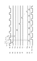
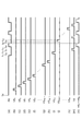
図6及び図7は、第1実施形態に係る固体撮像素子の制御方法において固体撮像素子11に付与される各信号のタイミングチャートである。図6は、受光領域20の全ての画素から電荷を読み出すモード(通常読み出しモード)を示している。また、図7は、受光領域20のうち一部の領域(関心領域)の画素のみから電荷を読み出すモード(部分読み出しモード)を示している。
第1の制御方法(通常読み出しモード)では、受光領域20の全ての画素P1,1〜PM,Nに蓄積された電荷を読み出す。図6に示されるように、まず、時刻t10から時刻t11までの期間、制御部6がリセット制御信号REをハイレベルとする。これにより、N個の積分回路42それぞれにおいて、放電用スイッチ42cが閉状態となり、容量素子42bが放電される。
第2の制御方法(部分読み出しモード)では、受光領域20の画素P1,1〜PM,Nのうち一部の画素、すなわち読出対象行である第mp行から第M行に含まれる画素Pmp,1〜PM,N(但し、ここではmpは3以上(M−1)以下の奇数とする)に蓄積された電荷を読み出し、非読出対象行である残りの第1行から第(mp−1)行に含まれる画素P1,1〜Pmp−1,Nに蓄積された電荷については排出処理(リセット)を行う。
続いて、本発明に係る固体撮像素子の制御方法に関する第2実施形態について説明する。なお、本実施形態において、第1の制御方法(通常読み出しモード)は前述した第1実施形態と同様なので、その説明を省略する。
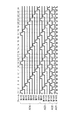
図10は、第2実施形態に係る固体撮像素子の制御方法において固体撮像素子11に付与される各信号のタイミングチャートであって、受光領域20のうち一部の領域(関心領域)の画素のみから電荷を読み出すモード(部分読み出しモード)を示している。図10の(a)〜(n)には、第1実施形態の図7の(a)〜(n)に相当する各信号が示されている。
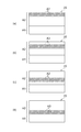
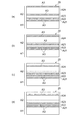
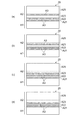
上述した各実施形態では、2回の撮像フレームの間に非読出対象行の画素を一回ずつリセットできるように、各撮像フレームにおいて奇数番目及び偶数番目の非読出対象行を交互にリセットする場合を例示した。図12は、このような制御方法における非読出対象行のリセットの様子を模式的に示す図である。図12(a)〜(d)それぞれは、4つの連続する撮像フレームそれぞれを示しており、各図には、一又は二以上の読出対象行からなる関心領域A1と、二以上の非読出対象行からなる非関心領域A2と、各撮像フレームにおいてリセット対象となる非読出対象行A3とが示されている。図12に示されるように、上述した各実施形態では、第1撮像フレーム(図12(a))及び第3撮像フレーム(図12(c))において奇数番目の非読出対象行A3がリセットされ、第2撮像フレーム(図12(b))及び第4撮像フレーム(図12(d))において偶数番目の非読出対象行A3がリセットされる。
Claims (7)
- フォトダイオード、及び該フォトダイオードに一端が接続された読出用スイッチを各々含むM×N個(Mは3以上の整数、Nは2以上の整数)の画素がM行N列に2次元配列されて成る受光領域を備える固体撮像素子の制御方法であって、
前記受光領域のうち一部の領域を構成する一又は複数の行(以下、読出対象行という)に含まれる前記画素に蓄積された電荷を、L回(Lは2以上の整数)の撮像フレームの各々において選択的に読み出すとともに、
前記L回の撮像フレームのそれぞれにおいて、前記読出対象行を除く他の二以上の行(以下、非読出対象行という)のうち一部の前記非読出対象行に含まれる前記画素に蓄積された電荷の排出処理を行い、且つ、前記二以上の非読出対象行の各々について前記L回の撮像フレームの間に少なくとも一回、前記排出処理を行うことを特徴とする、固体撮像素子の制御方法。 - 前記読出対象行に隣接する一又は複数の前記非読出対象行の前記排出処理の頻度が、他の前記非読出対象行の前記排出処理の頻度より多いことを特徴とする、請求項1に記載の固体撮像素子の制御方法。
- 前記一部の非読出対象行が複数行存在しており、
前記L回の撮像フレームのそれぞれにおいて、前記一部の非読出対象行に含まれる前記画素に蓄積された電荷の排出処理を同時に行うことを特徴とする、請求項1または2に記載の固体撮像素子の制御方法。 - 前記一部の非読出対象行が複数行存在しており、
前記L回の撮像フレームのそれぞれにおいて、前記一部の非読出対象行に含まれる前記画素に蓄積された電荷の排出処理を逐次に行うことを特徴とする、請求項1または2に記載の固体撮像素子の制御方法。 - 前記一部の非読出対象行が複数行存在しており、
前記L回の撮像フレームのそれぞれにおいて、前記一部の非読出対象行同士の間隔を1行以上あけることを特徴とする、請求項1〜4のいずれか一項に記載の固体撮像素子の制御方法。 - フォトダイオード、及び該フォトダイオードに一端が接続された読出用スイッチを各々含むM×N個(Mは3以上の整数、Nは2以上の整数)の画素がM行N列に2次元配列されて成る受光領域を備える固体撮像素子の制御方法であって、
前記受光領域のうち一部の領域を構成する一又は複数の行(以下、読出対象行という)に含まれる前記画素に蓄積された電荷を、L回(Lは2以上の整数)の撮像フレームの各々において選択的に読み出すとともに、
前記L回の撮像フレームのそれぞれにおいて、前記読出対象行を除く他の行(以下、非読出対象行という)に含まれる二以上の行のうち一部の行に含まれる前記画素に蓄積された電荷の排出処理を行い、且つ、前記二以上の行の各々について前記L回の撮像フレームの間に少なくとも一回、前記排出処理を行うことを特徴とする、固体撮像素子の制御方法。 - 前記L回の撮像フレームにおいて、前記非読出対象行のうち前記二以上の行を除く他の行に含まれる前記画素に蓄積された電荷の排出処理を行わないことを特徴とする、請求項6に記載の固体撮像素子の制御方法。
Priority Applications (7)
| Application Number | Priority Date | Filing Date | Title |
|---|---|---|---|
| JP2011123574A JP5714982B2 (ja) | 2011-02-01 | 2011-06-01 | 固体撮像素子の制御方法 |
| EP18174796.5A EP3386187B1 (en) | 2011-02-01 | 2011-12-14 | Method for controlling solid-state image pickup device |
| US13/982,527 US9197826B2 (en) | 2011-02-01 | 2011-12-14 | Method for controlling solid-state image pickup device |
| PCT/JP2011/078954 WO2012105129A1 (ja) | 2011-02-01 | 2011-12-14 | 固体撮像素子の制御方法 |
| KR1020137022308A KR101928115B1 (ko) | 2011-02-01 | 2011-12-14 | 고체 촬상 소자의 제어 방법 |
| CN201180066659.1A CN103339928B (zh) | 2011-02-01 | 2011-12-14 | 固体摄像元件的控制方法 |
| EP11857771.7A EP2672700B1 (en) | 2011-02-01 | 2011-12-14 | Method for controlling solid-state image pickup device |
Applications Claiming Priority (3)
| Application Number | Priority Date | Filing Date | Title |
|---|---|---|---|
| JP2011019988 | 2011-02-01 | ||
| JP2011019988 | 2011-02-01 | ||
| JP2011123574A JP5714982B2 (ja) | 2011-02-01 | 2011-06-01 | 固体撮像素子の制御方法 |
Related Child Applications (1)
| Application Number | Title | Priority Date | Filing Date |
|---|---|---|---|
| JP2015049629A Division JP5749873B1 (ja) | 2011-02-01 | 2015-03-12 | 固体撮像素子の制御方法 |
Publications (2)
| Publication Number | Publication Date |
|---|---|
| JP2012178812A true JP2012178812A (ja) | 2012-09-13 |
| JP5714982B2 JP5714982B2 (ja) | 2015-05-07 |
Family
ID=46602359
Family Applications (1)
| Application Number | Title | Priority Date | Filing Date |
|---|---|---|---|
| JP2011123574A Active JP5714982B2 (ja) | 2011-02-01 | 2011-06-01 | 固体撮像素子の制御方法 |
Country Status (6)
| Country | Link |
|---|---|
| US (1) | US9197826B2 (ja) |
| EP (2) | EP3386187B1 (ja) |
| JP (1) | JP5714982B2 (ja) |
| KR (1) | KR101928115B1 (ja) |
| CN (1) | CN103339928B (ja) |
| WO (1) | WO2012105129A1 (ja) |
Cited By (2)
| Publication number | Priority date | Publication date | Assignee | Title |
|---|---|---|---|---|
| KR101732301B1 (ko) | 2013-04-30 | 2017-05-02 | 후지필름 가부시키가이샤 | 고체 촬상 소자 및 촬상 장치 |
| KR101760200B1 (ko) * | 2013-06-04 | 2017-07-20 | 후지필름 가부시키가이샤 | 고체 촬상 소자 및 촬상 장치 |
Families Citing this family (9)
| Publication number | Priority date | Publication date | Assignee | Title |
|---|---|---|---|---|
| JPH062380B2 (ja) | 1988-05-20 | 1994-01-12 | 本州製紙株式会社 | 学習計測による段ボール生産プロセスのロット替え制御方法 |
| JP5730030B2 (ja) * | 2011-01-17 | 2015-06-03 | 浜松ホトニクス株式会社 | 固体撮像装置 |
| FR3006500B1 (fr) * | 2013-06-04 | 2016-10-28 | Centre Nat De La Rech Scient - Cnrs - | Capteur cmos a photosites standard |
| JP6184761B2 (ja) * | 2013-06-11 | 2017-08-23 | 浜松ホトニクス株式会社 | 固体撮像装置 |
| US9297998B2 (en) * | 2014-03-28 | 2016-03-29 | Amazon Technologies, Inc. | Electrode of an electrowetting device |
| JP6664122B2 (ja) * | 2014-08-20 | 2020-03-13 | パナソニックIpマネジメント株式会社 | 固体撮像装置及びカメラ |
| JP2017143092A (ja) * | 2016-02-08 | 2017-08-17 | ソニー株式会社 | ガラスインタポーザモジュール、撮像装置、および電子機器 |
| US10438332B2 (en) * | 2017-05-18 | 2019-10-08 | Semiconductor Components Industries, Llc | Methods and apparatus for selective pixel readout for image transformation |
| CN109037250B (zh) * | 2017-06-12 | 2021-11-05 | 上海耕岩智能科技有限公司 | 一种影像侦测显示装置、器件及其制备方法 |
Citations (3)
| Publication number | Priority date | Publication date | Assignee | Title |
|---|---|---|---|---|
| JPH09321267A (ja) * | 1996-02-22 | 1997-12-12 | Canon Inc | 光電変換装置の駆動方法及び光電変換装置 |
| JP2009165051A (ja) * | 2008-01-10 | 2009-07-23 | Canon Inc | 固体撮像装置、撮像システム、及び固体撮像装置の駆動方法 |
| JP2010518746A (ja) * | 2007-02-09 | 2010-05-27 | ジェンテックス コーポレイション | 改良型撮像装置 |
Family Cites Families (7)
| Publication number | Priority date | Publication date | Assignee | Title |
|---|---|---|---|---|
| JPH11318877A (ja) | 1998-01-29 | 1999-11-24 | Toshiba Corp | X線平面検出器を用いたx線診断装置及びx線診断装置の制御方法 |
| JP2005184777A (ja) * | 2003-11-28 | 2005-07-07 | Sanyo Electric Co Ltd | スミア演算回路、撮像装置、及び固体撮像素子の駆動方法 |
| JP2005184358A (ja) * | 2003-12-18 | 2005-07-07 | Sony Corp | 固体撮像装置、及び画素信号読み出し方法 |
| JP2007158741A (ja) * | 2005-12-06 | 2007-06-21 | Olympus Corp | 固体撮像装置 |
| JP5101946B2 (ja) * | 2007-08-03 | 2012-12-19 | キヤノン株式会社 | 撮像装置及び撮像システム |
| JP5272630B2 (ja) | 2008-10-03 | 2013-08-28 | ソニー株式会社 | 固体撮像素子およびその駆動方法、並びにカメラシステム |
| JP5284132B2 (ja) * | 2009-02-06 | 2013-09-11 | キヤノン株式会社 | 固体撮像装置、撮像システム、および撮像装置の駆動方法 |
-
2011
- 2011-06-01 JP JP2011123574A patent/JP5714982B2/ja active Active
- 2011-12-14 EP EP18174796.5A patent/EP3386187B1/en active Active
- 2011-12-14 CN CN201180066659.1A patent/CN103339928B/zh active Active
- 2011-12-14 KR KR1020137022308A patent/KR101928115B1/ko active Active
- 2011-12-14 US US13/982,527 patent/US9197826B2/en active Active
- 2011-12-14 WO PCT/JP2011/078954 patent/WO2012105129A1/ja not_active Ceased
- 2011-12-14 EP EP11857771.7A patent/EP2672700B1/en active Active
Patent Citations (3)
| Publication number | Priority date | Publication date | Assignee | Title |
|---|---|---|---|---|
| JPH09321267A (ja) * | 1996-02-22 | 1997-12-12 | Canon Inc | 光電変換装置の駆動方法及び光電変換装置 |
| JP2010518746A (ja) * | 2007-02-09 | 2010-05-27 | ジェンテックス コーポレイション | 改良型撮像装置 |
| JP2009165051A (ja) * | 2008-01-10 | 2009-07-23 | Canon Inc | 固体撮像装置、撮像システム、及び固体撮像装置の駆動方法 |
Cited By (2)
| Publication number | Priority date | Publication date | Assignee | Title |
|---|---|---|---|---|
| KR101732301B1 (ko) | 2013-04-30 | 2017-05-02 | 후지필름 가부시키가이샤 | 고체 촬상 소자 및 촬상 장치 |
| KR101760200B1 (ko) * | 2013-06-04 | 2017-07-20 | 후지필름 가부시키가이샤 | 고체 촬상 소자 및 촬상 장치 |
Also Published As
| Publication number | Publication date |
|---|---|
| CN103339928A (zh) | 2013-10-02 |
| EP2672700A4 (en) | 2017-01-18 |
| EP2672700B1 (en) | 2018-06-13 |
| EP3386187B1 (en) | 2021-01-20 |
| EP2672700A1 (en) | 2013-12-11 |
| EP3386187A1 (en) | 2018-10-10 |
| KR20140006912A (ko) | 2014-01-16 |
| KR101928115B1 (ko) | 2018-12-11 |
| JP5714982B2 (ja) | 2015-05-07 |
| WO2012105129A1 (ja) | 2012-08-09 |
| US20130308030A1 (en) | 2013-11-21 |
| CN103339928B (zh) | 2016-10-19 |
| US9197826B2 (en) | 2015-11-24 |
Similar Documents
| Publication | Publication Date | Title |
|---|---|---|
| JP5714982B2 (ja) | 固体撮像素子の制御方法 | |
| US9369643B2 (en) | Solid-state imaging device | |
| JP6184761B2 (ja) | 固体撮像装置 | |
| US9049394B2 (en) | Solid imaging device | |
| JP5749873B1 (ja) | 固体撮像素子の制御方法 | |
| KR101821444B1 (ko) | 고체 촬상 장치 및 고체 촬상 장치의 구동 방법 | |
| KR101916484B1 (ko) | 고체 촬상 장치 및 고체 촬상 장치의 구동 방법 |
Legal Events
| Date | Code | Title | Description |
|---|---|---|---|
| A621 | Written request for application examination |
Free format text: JAPANESE INTERMEDIATE CODE: A621 Effective date: 20140212 |
|
| TRDD | Decision of grant or rejection written | ||
| A01 | Written decision to grant a patent or to grant a registration (utility model) |
Free format text: JAPANESE INTERMEDIATE CODE: A01 Effective date: 20150210 |
|
| A61 | First payment of annual fees (during grant procedure) |
Free format text: JAPANESE INTERMEDIATE CODE: A61 Effective date: 20150312 |
|
| R150 | Certificate of patent or registration of utility model |
Ref document number: 5714982 Country of ref document: JP Free format text: JAPANESE INTERMEDIATE CODE: R150 |
|
| R250 | Receipt of annual fees |
Free format text: JAPANESE INTERMEDIATE CODE: R250 |
|
| R250 | Receipt of annual fees |
Free format text: JAPANESE INTERMEDIATE CODE: R250 |
|
| R250 | Receipt of annual fees |
Free format text: JAPANESE INTERMEDIATE CODE: R250 |