JP2012190903A - 気相成長装置、及び気相成長方法 - Google Patents
気相成長装置、及び気相成長方法 Download PDFInfo
- Publication number
- JP2012190903A JP2012190903A JP2011051550A JP2011051550A JP2012190903A JP 2012190903 A JP2012190903 A JP 2012190903A JP 2011051550 A JP2011051550 A JP 2011051550A JP 2011051550 A JP2011051550 A JP 2011051550A JP 2012190903 A JP2012190903 A JP 2012190903A
- Authority
- JP
- Japan
- Prior art keywords
- gas
- gas introduction
- reaction
- vapor phase
- reaction tube
- Prior art date
- Legal status (The legal status is an assumption and is not a legal conclusion. Google has not performed a legal analysis and makes no representation as to the accuracy of the status listed.)
- Granted
Links
Images


Classifications
-
- C—CHEMISTRY; METALLURGY
- C23—COATING METALLIC MATERIAL; COATING MATERIAL WITH METALLIC MATERIAL; CHEMICAL SURFACE TREATMENT; DIFFUSION TREATMENT OF METALLIC MATERIAL; COATING BY VACUUM EVAPORATION, BY SPUTTERING, BY ION IMPLANTATION OR BY CHEMICAL VAPOUR DEPOSITION, IN GENERAL; INHIBITING CORROSION OF METALLIC MATERIAL OR INCRUSTATION IN GENERAL
- C23C—COATING METALLIC MATERIAL; COATING MATERIAL WITH METALLIC MATERIAL; SURFACE TREATMENT OF METALLIC MATERIAL BY DIFFUSION INTO THE SURFACE, BY CHEMICAL CONVERSION OR SUBSTITUTION; COATING BY VACUUM EVAPORATION, BY SPUTTERING, BY ION IMPLANTATION OR BY CHEMICAL VAPOUR DEPOSITION, IN GENERAL
- C23C16/00—Chemical coating by decomposition of gaseous compounds, without leaving reaction products of surface material in the coating, i.e. chemical vapour deposition [CVD] processes
- C23C16/44—Chemical coating by decomposition of gaseous compounds, without leaving reaction products of surface material in the coating, i.e. chemical vapour deposition [CVD] processes characterised by the method of coating
- C23C16/455—Chemical coating by decomposition of gaseous compounds, without leaving reaction products of surface material in the coating, i.e. chemical vapour deposition [CVD] processes characterised by the method of coating characterised by the method used for introducing gases into reaction chamber or for modifying gas flows in reaction chamber
- C23C16/45563—Gas nozzles
- C23C16/45565—Shower nozzles
-
- C—CHEMISTRY; METALLURGY
- C23—COATING METALLIC MATERIAL; COATING MATERIAL WITH METALLIC MATERIAL; CHEMICAL SURFACE TREATMENT; DIFFUSION TREATMENT OF METALLIC MATERIAL; COATING BY VACUUM EVAPORATION, BY SPUTTERING, BY ION IMPLANTATION OR BY CHEMICAL VAPOUR DEPOSITION, IN GENERAL; INHIBITING CORROSION OF METALLIC MATERIAL OR INCRUSTATION IN GENERAL
- C23C—COATING METALLIC MATERIAL; COATING MATERIAL WITH METALLIC MATERIAL; SURFACE TREATMENT OF METALLIC MATERIAL BY DIFFUSION INTO THE SURFACE, BY CHEMICAL CONVERSION OR SUBSTITUTION; COATING BY VACUUM EVAPORATION, BY SPUTTERING, BY ION IMPLANTATION OR BY CHEMICAL VAPOUR DEPOSITION, IN GENERAL
- C23C16/00—Chemical coating by decomposition of gaseous compounds, without leaving reaction products of surface material in the coating, i.e. chemical vapour deposition [CVD] processes
- C23C16/22—Chemical coating by decomposition of gaseous compounds, without leaving reaction products of surface material in the coating, i.e. chemical vapour deposition [CVD] processes characterised by the deposition of inorganic material, other than metallic material
- C23C16/30—Deposition of compounds, mixtures or solid solutions, e.g. borides, carbides, nitrides
- C23C16/301—AIII BV compounds, where A is Al, Ga, In or Tl and B is N, P, As, Sb or Bi
- C23C16/303—Nitrides
-
- H—ELECTRICITY
- H10—SEMICONDUCTOR DEVICES; ELECTRIC SOLID-STATE DEVICES NOT OTHERWISE PROVIDED FOR
- H10P—GENERIC PROCESSES OR APPARATUS FOR THE MANUFACTURE OR TREATMENT OF DEVICES COVERED BY CLASS H10
- H10P14/00—Formation of materials, e.g. in the shape of layers or pillars
- H10P14/20—Formation of materials, e.g. in the shape of layers or pillars of semiconductor materials
- H10P14/24—Formation of materials, e.g. in the shape of layers or pillars of semiconductor materials using chemical vapour deposition [CVD]
-
- H—ELECTRICITY
- H10—SEMICONDUCTOR DEVICES; ELECTRIC SOLID-STATE DEVICES NOT OTHERWISE PROVIDED FOR
- H10P—GENERIC PROCESSES OR APPARATUS FOR THE MANUFACTURE OR TREATMENT OF DEVICES COVERED BY CLASS H10
- H10P14/00—Formation of materials, e.g. in the shape of layers or pillars
- H10P14/20—Formation of materials, e.g. in the shape of layers or pillars of semiconductor materials
- H10P14/32—Formation of materials, e.g. in the shape of layers or pillars of semiconductor materials characterised by intermediate layers between substrates and deposited layers
- H10P14/3202—Materials thereof
- H10P14/3214—Materials thereof being Group IIIA-VA semiconductors
- H10P14/3216—Nitrides
-
- H—ELECTRICITY
- H10—SEMICONDUCTOR DEVICES; ELECTRIC SOLID-STATE DEVICES NOT OTHERWISE PROVIDED FOR
- H10P—GENERIC PROCESSES OR APPARATUS FOR THE MANUFACTURE OR TREATMENT OF DEVICES COVERED BY CLASS H10
- H10P14/00—Formation of materials, e.g. in the shape of layers or pillars
- H10P14/20—Formation of materials, e.g. in the shape of layers or pillars of semiconductor materials
- H10P14/34—Deposited materials, e.g. layers
- H10P14/3402—Deposited materials, e.g. layers characterised by the chemical composition
- H10P14/3414—Deposited materials, e.g. layers characterised by the chemical composition being group IIIA-VIA materials
- H10P14/3416—Nitrides
-
- H—ELECTRICITY
- H10—SEMICONDUCTOR DEVICES; ELECTRIC SOLID-STATE DEVICES NOT OTHERWISE PROVIDED FOR
- H10P—GENERIC PROCESSES OR APPARATUS FOR THE MANUFACTURE OR TREATMENT OF DEVICES COVERED BY CLASS H10
- H10P14/00—Formation of materials, e.g. in the shape of layers or pillars
- H10P14/20—Formation of materials, e.g. in the shape of layers or pillars of semiconductor materials
- H10P14/34—Deposited materials, e.g. layers
- H10P14/3438—Doping during depositing
- H10P14/3441—Conductivity type
Landscapes
- Chemical & Material Sciences (AREA)
- General Chemical & Material Sciences (AREA)
- Chemical Kinetics & Catalysis (AREA)
- Engineering & Computer Science (AREA)
- Materials Engineering (AREA)
- Mechanical Engineering (AREA)
- Metallurgy (AREA)
- Organic Chemistry (AREA)
- Inorganic Chemistry (AREA)
- Chemical Vapour Deposition (AREA)
Abstract
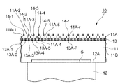
【解決手段】実施形態の気相成長装置は、複数のガス導入部、及びこれら複数のガス導入部の下方に位置するガス反応部を含む反応管と、前記反応管の、前記ガス反応部の内部に表面が露出し、前記表面に基板を載置及び固定するためのサセプタとを具える。また、前記反応管の、前記複数のガス導入部及び前記ガス反応部間に設けられた整流板と、前記反応管の、前記複数のガス導入部それぞれに接続されてなる複数のガス導入菅と、前記反応管の外部において、前記複数のガス導入管それぞれに供給すべきガスを切り替えるための切替装置と、を具える。
【選択図】図1
Description
11 反応管
11A(11A−1〜11A−r) ガス導入部
11B ガス反応部
12 サセプタ
13 整流板
13A−1〜13A−p ガス供給口
14−1〜14−r ガス導入管
20 切替装置
21 第1の切替素子
22 第2の切替素子
23 第3の切替素子
Claims (6)
- 複数のガス導入部、及びこれら複数のガス導入部の下方に位置するガス反応部を含む反応管と、
前記反応管の、前記ガス反応部の内部に表面が露出し、前記表面に基板を載置及び固定するためのサセプタと、
前記反応管の、前記複数のガス導入部及び前記ガス反応部間に設けられた整流板と、
前記反応管の、前記複数のガス導入部それぞれに接続されてなる複数のガス導入菅と、
前記反応管の外部において、前記複数のガス導入管それぞれに供給すべきガスを切り替えるための切替装置と、
を具えることを特徴とする、気相成長装置。 - 前記切替装置は、前記複数のガス導入菅それぞれに供給すべき原料ガス及びキャリアガスの切り替えを行い、前記反応管の前記ガス導入部に供給する前記原料ガスの流量を制御するように構成したことを特徴とする、請求項1に記載の気相成長装置。
- 前記複数のガス導入部は、前記整流板のガス供給口の配列方向に対して並列に配列されてなることを特徴とする、請求項1又は2に記載の気相成長装置。
- 前記原料ガスは、II族ガス、III族ガス、IV族ガス、V族ガス及びVI族ガスからなる群より選ばれる少なくとも一種であることを特徴とする、請求項1〜3のいずれか一に記載の気相成長装置。
- 前記キャリアガスは、窒素ガス、水素ガス及びアルゴンガスからなる群より選ばれる少なくとも一種であることを特徴とする、請求項1〜4のいずれか一に記載の気相成長装置。
- 複数のガス導入部、及びこれら複数のガス導入部の下方に位置するガス反応部を含む反応管の、前記ガス反応部の内部に表面が露出したサセプタ上に基板を載置及び固定する工程と、
前記反応管の、前記複数のガス導入部それぞれに接続されてなる複数のガス導入管から、前記反応管の、前記複数のガス導入部及び前記ガス反応部間に設けられた整流板を介して、前記ガス反応部における前記基板に対して原料ガス及びキャリアガスを第1の流量比で供給し、前記基板上において第1の膜体を形成する工程と、
前記反応管の外部に設けられた前記複数のガス導入管それぞれに供給すべきガスを切り替えるための切替装置によって、前記複数のガス導入管それぞれに供給すべき原料ガス及びキャリアガスの切り替えを行い、前記ガス反応部における前記基板に対して原料ガス及びキャリアガスを前記第1の流量比と異なる第2の流量比で供給し、前記基板の前記第1の膜体上に第2の膜体を形成する工程と、
を具えることを特徴とする、気相成長方法。
Priority Applications (2)
| Application Number | Priority Date | Filing Date | Title |
|---|---|---|---|
| JP2011051550A JP5481416B2 (ja) | 2011-03-09 | 2011-03-09 | 気相成長装置、及び気相成長方法 |
| US13/220,273 US8835331B2 (en) | 2011-03-09 | 2011-08-29 | Vapor-phase growing apparatus and vapor-phase growing method |
Applications Claiming Priority (1)
| Application Number | Priority Date | Filing Date | Title |
|---|---|---|---|
| JP2011051550A JP5481416B2 (ja) | 2011-03-09 | 2011-03-09 | 気相成長装置、及び気相成長方法 |
Publications (2)
| Publication Number | Publication Date |
|---|---|
| JP2012190903A true JP2012190903A (ja) | 2012-10-04 |
| JP5481416B2 JP5481416B2 (ja) | 2014-04-23 |
Family
ID=46795957
Family Applications (1)
| Application Number | Title | Priority Date | Filing Date |
|---|---|---|---|
| JP2011051550A Expired - Fee Related JP5481416B2 (ja) | 2011-03-09 | 2011-03-09 | 気相成長装置、及び気相成長方法 |
Country Status (2)
| Country | Link |
|---|---|
| US (1) | US8835331B2 (ja) |
| JP (1) | JP5481416B2 (ja) |
Cited By (1)
| Publication number | Priority date | Publication date | Assignee | Title |
|---|---|---|---|---|
| JP2015015430A (ja) * | 2013-07-08 | 2015-01-22 | 株式会社ニューフレアテクノロジー | 気相成長装置および気相成長方法 |
Families Citing this family (2)
| Publication number | Priority date | Publication date | Assignee | Title |
|---|---|---|---|---|
| CN103757606A (zh) * | 2013-12-31 | 2014-04-30 | 南昌黄绿照明有限公司 | 一种mocvd气路压差控制系统 |
| JP2016081945A (ja) * | 2014-10-09 | 2016-05-16 | 株式会社ニューフレアテクノロジー | 気相成長装置および気相成長方法 |
Citations (4)
| Publication number | Priority date | Publication date | Assignee | Title |
|---|---|---|---|---|
| JPH04337627A (ja) * | 1991-05-15 | 1992-11-25 | Fujitsu Ltd | 気相成長装置 |
| JP2002016008A (ja) * | 2000-06-30 | 2002-01-18 | Toshiba Ceramics Co Ltd | 薄膜気相成長方法及び薄膜気相成長装置 |
| JP2002075879A (ja) * | 2000-09-01 | 2002-03-15 | Inst Of Physical & Chemical Res | 半導体の不純物ドーピング方法、その装置および半導体材料 |
| JP2009302507A (ja) * | 2008-05-15 | 2009-12-24 | Stanley Electric Co Ltd | 成膜装置および半導体素子の製造方法 |
Family Cites Families (4)
| Publication number | Priority date | Publication date | Assignee | Title |
|---|---|---|---|---|
| JP2804959B2 (ja) | 1992-09-21 | 1998-09-30 | 株式会社ジャパンエナジー | Ш−v族化合物半導体のエピタキシャル成長方法 |
| US6645884B1 (en) * | 1999-07-09 | 2003-11-11 | Applied Materials, Inc. | Method of forming a silicon nitride layer on a substrate |
| US8231799B2 (en) * | 2006-04-28 | 2012-07-31 | Applied Materials, Inc. | Plasma reactor apparatus with multiple gas injection zones having time-changing separate configurable gas compositions for each zone |
| US8501600B2 (en) * | 2010-09-27 | 2013-08-06 | Applied Materials, Inc. | Methods for depositing germanium-containing layers |
-
2011
- 2011-03-09 JP JP2011051550A patent/JP5481416B2/ja not_active Expired - Fee Related
- 2011-08-29 US US13/220,273 patent/US8835331B2/en active Active
Patent Citations (4)
| Publication number | Priority date | Publication date | Assignee | Title |
|---|---|---|---|---|
| JPH04337627A (ja) * | 1991-05-15 | 1992-11-25 | Fujitsu Ltd | 気相成長装置 |
| JP2002016008A (ja) * | 2000-06-30 | 2002-01-18 | Toshiba Ceramics Co Ltd | 薄膜気相成長方法及び薄膜気相成長装置 |
| JP2002075879A (ja) * | 2000-09-01 | 2002-03-15 | Inst Of Physical & Chemical Res | 半導体の不純物ドーピング方法、その装置および半導体材料 |
| JP2009302507A (ja) * | 2008-05-15 | 2009-12-24 | Stanley Electric Co Ltd | 成膜装置および半導体素子の製造方法 |
Cited By (1)
| Publication number | Priority date | Publication date | Assignee | Title |
|---|---|---|---|---|
| JP2015015430A (ja) * | 2013-07-08 | 2015-01-22 | 株式会社ニューフレアテクノロジー | 気相成長装置および気相成長方法 |
Also Published As
| Publication number | Publication date |
|---|---|
| US8835331B2 (en) | 2014-09-16 |
| US20120231610A1 (en) | 2012-09-13 |
| JP5481416B2 (ja) | 2014-04-23 |
Similar Documents
| Publication | Publication Date | Title |
|---|---|---|
| US4659401A (en) | Growth of epitaxial films by plasma enchanced chemical vapor deposition (PE-CVD) | |
| JP4840832B2 (ja) | 気相成長装置、気相成長方法、および半導体素子の製造方法 | |
| US20080050889A1 (en) | Hotwall reactor and method for reducing particle formation in GaN MOCVD | |
| US8815717B2 (en) | Vapor deposition method and vapor deposition apparatus | |
| WO2020149083A1 (ja) | 半導体製造装置 | |
| US4773355A (en) | Growth of epitaxial films by chemical vapor deposition | |
| JP5042053B2 (ja) | 有機金属気相成長炉 | |
| JP5481416B2 (ja) | 気相成長装置、及び気相成長方法 | |
| JP5481415B2 (ja) | 気相成長装置、及び気相成長方法 | |
| JP2011222592A (ja) | 気相成長装置及び気相成長方法 | |
| CN101924023A (zh) | Iii族氮化物半导体的气相生长装置 | |
| JPH09102461A (ja) | 気相成長装置 | |
| JP6796172B2 (ja) | 気相成長装置及び気相成長方法 | |
| JP4663912B2 (ja) | 半導体製造装置 | |
| JP5546296B2 (ja) | 気相成長装置、材料ガス層流を基板上に水平に供給するノズル、及び気相成長方法 | |
| US11021789B2 (en) | MOCVD system injector for fast growth of AlInGaBN material | |
| JP5110074B2 (ja) | 結晶の製造方法および発光素子の製造方法 | |
| JP3472976B2 (ja) | Iii族窒化物半導体の成膜方法およびその装置 | |
| JP2007242875A (ja) | 有機金属気相成長装置およびそれを用いた気相成長方法 | |
| JP2012084581A (ja) | 気相成長装置 | |
| US20130295283A1 (en) | Chemical vapor deposition apparatus with multiple inlets for controlling film thickness and uniformity | |
| JP6030907B2 (ja) | Iii族窒化物の製造方法 | |
| JP5321395B2 (ja) | 窒化物薄膜成膜装置 | |
| JP5524280B2 (ja) | 気相成長装置 | |
| US10000845B2 (en) | MOCVD system for growth of III-nitride and other semiconductors |
Legal Events
| Date | Code | Title | Description |
|---|---|---|---|
| A131 | Notification of reasons for refusal |
Free format text: JAPANESE INTERMEDIATE CODE: A131 Effective date: 20121120 |
|
| A977 | Report on retrieval |
Free format text: JAPANESE INTERMEDIATE CODE: A971007 Effective date: 20121122 |
|
| A521 | Request for written amendment filed |
Free format text: JAPANESE INTERMEDIATE CODE: A523 Effective date: 20130115 |
|
| A02 | Decision of refusal |
Free format text: JAPANESE INTERMEDIATE CODE: A02 Effective date: 20130416 |
|
| A521 | Request for written amendment filed |
Free format text: JAPANESE INTERMEDIATE CODE: A523 Effective date: 20130704 |
|
| A911 | Transfer to examiner for re-examination before appeal (zenchi) |
Free format text: JAPANESE INTERMEDIATE CODE: A911 Effective date: 20130711 |
|
| A131 | Notification of reasons for refusal |
Free format text: JAPANESE INTERMEDIATE CODE: A131 Effective date: 20130910 |
|
| A521 | Request for written amendment filed |
Free format text: JAPANESE INTERMEDIATE CODE: A523 Effective date: 20131105 |
|
| TRDD | Decision of grant or rejection written | ||
| A01 | Written decision to grant a patent or to grant a registration (utility model) |
Free format text: JAPANESE INTERMEDIATE CODE: A01 Effective date: 20140121 |
|
| A61 | First payment of annual fees (during grant procedure) |
Free format text: JAPANESE INTERMEDIATE CODE: A61 Effective date: 20140217 |
|
| R151 | Written notification of patent or utility model registration |
Ref document number: 5481416 Country of ref document: JP Free format text: JAPANESE INTERMEDIATE CODE: R151 |
|
| LAPS | Cancellation because of no payment of annual fees |