JP2012204518A - Deposition apparatus - Google Patents
Deposition apparatus Download PDFInfo
- Publication number
- JP2012204518A JP2012204518A JP2011066461A JP2011066461A JP2012204518A JP 2012204518 A JP2012204518 A JP 2012204518A JP 2011066461 A JP2011066461 A JP 2011066461A JP 2011066461 A JP2011066461 A JP 2011066461A JP 2012204518 A JP2012204518 A JP 2012204518A
- Authority
- JP
- Japan
- Prior art keywords
- film
- substrate
- gas
- adhesion promoter
- film forming
- Prior art date
- Legal status (The legal status is an assumption and is not a legal conclusion. Google has not performed a legal analysis and makes no representation as to the accuracy of the status listed.)
- Granted
Links
Images








Classifications
-
- C—CHEMISTRY; METALLURGY
- C23—COATING METALLIC MATERIAL; COATING MATERIAL WITH METALLIC MATERIAL; CHEMICAL SURFACE TREATMENT; DIFFUSION TREATMENT OF METALLIC MATERIAL; COATING BY VACUUM EVAPORATION, BY SPUTTERING, BY ION IMPLANTATION OR BY CHEMICAL VAPOUR DEPOSITION, IN GENERAL; INHIBITING CORROSION OF METALLIC MATERIAL OR INCRUSTATION IN GENERAL
- C23C—COATING METALLIC MATERIAL; COATING MATERIAL WITH METALLIC MATERIAL; SURFACE TREATMENT OF METALLIC MATERIAL BY DIFFUSION INTO THE SURFACE, BY CHEMICAL CONVERSION OR SUBSTITUTION; COATING BY VACUUM EVAPORATION, BY SPUTTERING, BY ION IMPLANTATION OR BY CHEMICAL VAPOUR DEPOSITION, IN GENERAL
- C23C16/00—Chemical coating by decomposition of gaseous compounds, without leaving reaction products of surface material in the coating, i.e. chemical vapour deposition [CVD] processes
- C23C16/44—Chemical coating by decomposition of gaseous compounds, without leaving reaction products of surface material in the coating, i.e. chemical vapour deposition [CVD] processes characterised by the method of coating
- C23C16/455—Chemical coating by decomposition of gaseous compounds, without leaving reaction products of surface material in the coating, i.e. chemical vapour deposition [CVD] processes characterised by the method of coating characterised by the method used for introducing gases into reaction chamber or for modifying gas flows in reaction chamber
-
- H—ELECTRICITY
- H10—SEMICONDUCTOR DEVICES; ELECTRIC SOLID-STATE DEVICES NOT OTHERWISE PROVIDED FOR
- H10P—GENERIC PROCESSES OR APPARATUS FOR THE MANUFACTURE OR TREATMENT OF DEVICES COVERED BY CLASS H10
- H10P14/00—Formation of materials, e.g. in the shape of layers or pillars
- H10P14/60—Formation of materials, e.g. in the shape of layers or pillars of insulating materials
- H10P14/68—Organic materials, e.g. photoresists
- H10P14/683—Organic materials, e.g. photoresists carbon-based polymeric organic materials, e.g. polyimides, poly cyclobutene or PVC
-
- C—CHEMISTRY; METALLURGY
- C23—COATING METALLIC MATERIAL; COATING MATERIAL WITH METALLIC MATERIAL; CHEMICAL SURFACE TREATMENT; DIFFUSION TREATMENT OF METALLIC MATERIAL; COATING BY VACUUM EVAPORATION, BY SPUTTERING, BY ION IMPLANTATION OR BY CHEMICAL VAPOUR DEPOSITION, IN GENERAL; INHIBITING CORROSION OF METALLIC MATERIAL OR INCRUSTATION IN GENERAL
- C23C—COATING METALLIC MATERIAL; COATING MATERIAL WITH METALLIC MATERIAL; SURFACE TREATMENT OF METALLIC MATERIAL BY DIFFUSION INTO THE SURFACE, BY CHEMICAL CONVERSION OR SUBSTITUTION; COATING BY VACUUM EVAPORATION, BY SPUTTERING, BY ION IMPLANTATION OR BY CHEMICAL VAPOUR DEPOSITION, IN GENERAL
- C23C16/00—Chemical coating by decomposition of gaseous compounds, without leaving reaction products of surface material in the coating, i.e. chemical vapour deposition [CVD] processes
- C23C16/44—Chemical coating by decomposition of gaseous compounds, without leaving reaction products of surface material in the coating, i.e. chemical vapour deposition [CVD] processes characterised by the method of coating
- C23C16/46—Chemical coating by decomposition of gaseous compounds, without leaving reaction products of surface material in the coating, i.e. chemical vapour deposition [CVD] processes characterised by the method of coating characterised by the method used for heating the substrate
- C23C16/463—Cooling of the substrate
- C23C16/466—Cooling of the substrate using thermal contact gas
-
- H—ELECTRICITY
- H10—SEMICONDUCTOR DEVICES; ELECTRIC SOLID-STATE DEVICES NOT OTHERWISE PROVIDED FOR
- H10P—GENERIC PROCESSES OR APPARATUS FOR THE MANUFACTURE OR TREATMENT OF DEVICES COVERED BY CLASS H10
- H10P14/00—Formation of materials, e.g. in the shape of layers or pillars
- H10P14/60—Formation of materials, e.g. in the shape of layers or pillars of insulating materials
- H10P14/63—Formation of materials, e.g. in the shape of layers or pillars of insulating materials characterised by the formation processes
- H10P14/6326—Deposition processes
- H10P14/6328—Deposition from the gas or vapour phase
- H10P14/6334—Deposition from the gas or vapour phase using decomposition or reaction of gaseous or vapour phase compounds, i.e. chemical vapour deposition
-
- H—ELECTRICITY
- H10—SEMICONDUCTOR DEVICES; ELECTRIC SOLID-STATE DEVICES NOT OTHERWISE PROVIDED FOR
- H10P—GENERIC PROCESSES OR APPARATUS FOR THE MANUFACTURE OR TREATMENT OF DEVICES COVERED BY CLASS H10
- H10P14/00—Formation of materials, e.g. in the shape of layers or pillars
- H10P14/60—Formation of materials, e.g. in the shape of layers or pillars of insulating materials
- H10P14/65—Formation of materials, e.g. in the shape of layers or pillars of insulating materials characterised by treatments performed before or after the formation of the materials
- H10P14/6502—Formation of materials, e.g. in the shape of layers or pillars of insulating materials characterised by treatments performed before or after the formation of the materials of treatments performed before formation of the materials
- H10P14/6512—Formation of materials, e.g. in the shape of layers or pillars of insulating materials characterised by treatments performed before or after the formation of the materials of treatments performed before formation of the materials by exposure to a gas or vapour
-
- H—ELECTRICITY
- H10—SEMICONDUCTOR DEVICES; ELECTRIC SOLID-STATE DEVICES NOT OTHERWISE PROVIDED FOR
- H10P—GENERIC PROCESSES OR APPARATUS FOR THE MANUFACTURE OR TREATMENT OF DEVICES COVERED BY CLASS H10
- H10P72/00—Handling or holding of wafers, substrates or devices during manufacture or treatment thereof
- H10P72/04—Apparatus for manufacture or treatment
- H10P72/0402—Apparatus for fluid treatment
-
- H—ELECTRICITY
- H10—SEMICONDUCTOR DEVICES; ELECTRIC SOLID-STATE DEVICES NOT OTHERWISE PROVIDED FOR
- H10P—GENERIC PROCESSES OR APPARATUS FOR THE MANUFACTURE OR TREATMENT OF DEVICES COVERED BY CLASS H10
- H10P72/00—Handling or holding of wafers, substrates or devices during manufacture or treatment thereof
- H10P72/04—Apparatus for manufacture or treatment
- H10P72/0431—Apparatus for thermal treatment
-
- H—ELECTRICITY
- H10—SEMICONDUCTOR DEVICES; ELECTRIC SOLID-STATE DEVICES NOT OTHERWISE PROVIDED FOR
- H10P—GENERIC PROCESSES OR APPARATUS FOR THE MANUFACTURE OR TREATMENT OF DEVICES COVERED BY CLASS H10
- H10P72/00—Handling or holding of wafers, substrates or devices during manufacture or treatment thereof
- H10P72/04—Apparatus for manufacture or treatment
- H10P72/0431—Apparatus for thermal treatment
- H10P72/0434—Apparatus for thermal treatment mainly by convection
-
- H—ELECTRICITY
- H10—SEMICONDUCTOR DEVICES; ELECTRIC SOLID-STATE DEVICES NOT OTHERWISE PROVIDED FOR
- H10P—GENERIC PROCESSES OR APPARATUS FOR THE MANUFACTURE OR TREATMENT OF DEVICES COVERED BY CLASS H10
- H10P72/00—Handling or holding of wafers, substrates or devices during manufacture or treatment thereof
- H10P72/06—Apparatus for monitoring, sorting, marking, testing or measuring
- H10P72/0602—Temperature monitoring
-
- H—ELECTRICITY
- H10—SEMICONDUCTOR DEVICES; ELECTRIC SOLID-STATE DEVICES NOT OTHERWISE PROVIDED FOR
- H10P—GENERIC PROCESSES OR APPARATUS FOR THE MANUFACTURE OR TREATMENT OF DEVICES COVERED BY CLASS H10
- H10P72/00—Handling or holding of wafers, substrates or devices during manufacture or treatment thereof
- H10P72/10—Handling or holding of wafers, substrates or devices during manufacture or treatment thereof using carriers specially adapted therefor, e.g. front opening unified pods [FOUP]
- H10P72/12—Vertical boat type carrier whereby the substrates are horizontally supported, e.g. comprising rod-shaped elements
-
- H—ELECTRICITY
- H10—SEMICONDUCTOR DEVICES; ELECTRIC SOLID-STATE DEVICES NOT OTHERWISE PROVIDED FOR
- H10P—GENERIC PROCESSES OR APPARATUS FOR THE MANUFACTURE OR TREATMENT OF DEVICES COVERED BY CLASS H10
- H10P72/00—Handling or holding of wafers, substrates or devices during manufacture or treatment thereof
- H10P72/30—Handling or holding of wafers, substrates or devices during manufacture or treatment thereof for conveying, e.g. between different workstations
- H10P72/33—Handling or holding of wafers, substrates or devices during manufacture or treatment thereof for conveying, e.g. between different workstations into and out of processing chamber
- H10P72/3312—Vertical transfer of a batch of workpieces
-
- B—PERFORMING OPERATIONS; TRANSPORTING
- B05—SPRAYING OR ATOMISING IN GENERAL; APPLYING FLUENT MATERIALS TO SURFACES, IN GENERAL
- B05D—PROCESSES FOR APPLYING FLUENT MATERIALS TO SURFACES, IN GENERAL
- B05D1/00—Processes for applying liquids or other fluent materials
- B05D1/36—Successively applying liquids or other fluent materials, e.g. without intermediate treatment
-
- B—PERFORMING OPERATIONS; TRANSPORTING
- B05—SPRAYING OR ATOMISING IN GENERAL; APPLYING FLUENT MATERIALS TO SURFACES, IN GENERAL
- B05D—PROCESSES FOR APPLYING FLUENT MATERIALS TO SURFACES, IN GENERAL
- B05D1/00—Processes for applying liquids or other fluent materials
- B05D1/60—Deposition of organic layers from vapour phase
-
- B—PERFORMING OPERATIONS; TRANSPORTING
- B05—SPRAYING OR ATOMISING IN GENERAL; APPLYING FLUENT MATERIALS TO SURFACES, IN GENERAL
- B05D—PROCESSES FOR APPLYING FLUENT MATERIALS TO SURFACES, IN GENERAL
- B05D3/00—Pretreatment of surfaces to which liquids or other fluent materials are to be applied; After-treatment of applied coatings, e.g. intermediate treating of an applied coating preparatory to subsequent applications of liquids or other fluent materials
- B05D3/10—Pretreatment of surfaces to which liquids or other fluent materials are to be applied; After-treatment of applied coatings, e.g. intermediate treating of an applied coating preparatory to subsequent applications of liquids or other fluent materials by other chemical means
- B05D3/104—Pretreatment of other substrates
Landscapes
- Chemical & Material Sciences (AREA)
- General Chemical & Material Sciences (AREA)
- Chemical Kinetics & Catalysis (AREA)
- Engineering & Computer Science (AREA)
- Materials Engineering (AREA)
- Mechanical Engineering (AREA)
- Metallurgy (AREA)
- Organic Chemistry (AREA)
- Chemical Vapour Deposition (AREA)
- Formation Of Insulating Films (AREA)
- Physical Vapour Deposition (AREA)
Abstract
【課題】成膜されたポリイミド膜の膜質を向上させるとともに、単位時間当たりに成膜処理される基板の枚数を増やすことができる成膜装置を提供する。
【解決手段】基板にポリイミド膜を成膜する成膜装置において、成膜容器60内に搬入されている基板を加熱する加熱機構62と、成膜容器60内に密着促進剤を気化させた密着促進剤ガスを供給する密着促進剤供給機構80と、加熱機構62と密着促進剤供給機構80とを制御する制御部100とを有する。制御部100は、基板を成膜容器60内に搬入した後、加熱機構62により、基板の温度を、基板にポリイミド膜を成膜するときの所定温度まで上昇させる間に、密着促進剤供給機構80により密着促進剤ガスを成膜容器60内に供給し、基板の表面を密着促進剤ガスにより処理するように、制御する。
【選択図】図4There is provided a film forming apparatus capable of improving the film quality of a formed polyimide film and increasing the number of substrates subjected to film forming processing per unit time.
In a film forming apparatus for forming a polyimide film on a substrate, a heating mechanism 62 for heating the substrate carried in the film forming container 60 and an adhesion in which an adhesion promoter is vaporized in the film forming container 60. It has an adhesion promoter supply mechanism 80 that supplies an accelerator gas, and a controller 100 that controls the heating mechanism 62 and the adhesion promoter supply mechanism 80. After the substrate is carried into the film forming container 60, the control unit 100 uses the heating mechanism 62 to raise the temperature of the substrate to a predetermined temperature when the polyimide film is formed on the substrate. The adhesion promoter gas is supplied into the film forming container 60 by 80, and the surface of the substrate is controlled to be treated with the adhesion promoter gas.
[Selection] Figure 4
Description
本発明は、基板に膜を成膜する成膜装置に関する。 The present invention relates to a film forming apparatus for forming a film on a substrate.
半導体デバイスに用いられる材料は、近年無機材料から有機材料へと幅を広げつつあり、無機材料にはない有機材料の特質等から半導体デバイスの特性や製造プロセスをより最適なものとすることができる。 In recent years, the materials used for semiconductor devices are expanding from inorganic materials to organic materials, and the characteristics and manufacturing processes of semiconductor devices can be optimized due to the characteristics of organic materials not found in inorganic materials. .
このような有機材料の1つとして、ポリイミドが挙げられる。ポリイミドは、絶縁性が高い。従って、基板の表面にポリイミドを成膜して得られるポリイミド膜は、絶縁膜として用いることができ、半導体デバイスにおける絶縁膜として用いることも可能である。 One such organic material is polyimide. Polyimide is highly insulating. Therefore, a polyimide film obtained by forming polyimide on the surface of a substrate can be used as an insulating film, and can also be used as an insulating film in a semiconductor device.
このようなポリイミド膜を成膜する方法としては、原料モノマーとして例えばピロメリット酸二無水物(PMDA)と、例えば4,4'−オキシジアニリン(ODA)を含む4,4'−ジアミノジフェニルエーテルを用いた蒸着重合による成膜方法が知られている。蒸着重合は、原料モノマーとして用いられるPMDA及びODAを基板の表面で熱重合反応させる方法である(例えば特許文献1参照)。特許文献1では、PMDA及びODAのモノマーを気化器で蒸発させ、蒸発させたそれぞれの蒸気を蒸着重合室に供給し、基板上で蒸着重合させてポリイミド膜を成膜する成膜方法が開示されている。
As a method for forming such a polyimide film, for example, pyromellitic dianhydride (PMDA) as a raw material monomer and 4,4′-diaminodiphenyl ether containing, for example, 4,4′-oxydianiline (ODA) are used. A film forming method by vapor deposition polymerization used is known. Vapor deposition polymerization is a method in which PMDA and ODA used as raw material monomers are subjected to a thermal polymerization reaction on the surface of a substrate (see, for example, Patent Document 1).
しかしながら、このようなPMDAガスとODAガスを基板に供給してポリイミド膜を成膜する成膜装置には、以下のような問題がある。 However, a film forming apparatus for forming a polyimide film by supplying such PMDA gas and ODA gas to the substrate has the following problems.
基板に成膜されたポリイミド膜の膜質を向上させるために、成膜前の密着促進剤による表面処理、成膜後の熱処理によるイミド化処理が必要である。 In order to improve the film quality of the polyimide film formed on the substrate, surface treatment with an adhesion promoter before film formation and imidization treatment by heat treatment after film formation are necessary.
密着促進剤による表面処理は、ポリイミド膜の成膜前に、基板表面を、例えばシランカップリング剤等の密着促進剤により処理するものである。これにより、成膜したポリイミド膜の密着力を向上させることができる。しかし、ポリイミド膜の成膜前に、ポリイミド膜の成膜を行う成膜容器とは別の処理容器内で、密着促進剤による表面処理を行う場合、工程数が増えて処理時間が増大し、単位時間当たりの処理枚数が低下する。 In the surface treatment with an adhesion promoter, the surface of the substrate is treated with an adhesion promoter such as a silane coupling agent before the polyimide film is formed. Thereby, the adhesive force of the formed polyimide film can be improved. However, when the surface treatment with the adhesion promoter is performed in a processing container different from the film forming container for forming the polyimide film before forming the polyimide film, the number of steps increases and the processing time increases. The number of processed sheets per unit time decreases.
また、成膜後の熱処理によるイミド化処理は、ポリイミド膜を成膜した後、更に熱処理し、膜中のポリイミドの割合であるイミド化率を上昇させるためのものである。これにより、成膜したポリイミド膜の絶縁性を向上させることができる。しかし、成膜後、成膜容器から搬出した基板を、例えばバッチ処理可能な縦型炉等の熱処理装置を用いて熱処理する場合、ボートに保持されている基板を加熱して温度を上昇させるために時間を要する。 The imidation treatment by heat treatment after film formation is for further heat treatment after film formation of the polyimide film to increase the imidation ratio, which is the ratio of polyimide in the film. Thereby, the insulation of the formed polyimide film can be improved. However, when the substrate unloaded from the deposition container after film formation is heat-treated using a heat treatment apparatus such as a vertical furnace capable of batch processing, the substrate held in the boat is heated to raise the temperature. Takes time.
一方、例えば枚葉処理可能なホットプレート等の熱処理装置により熱処理する場合には、バッチ処理可能な熱処理装置により熱処理する場合に比べ、熱処理に要する時間は短くなる。しかし、枚葉処理であるため、ロット全体を処理するのに非常に長い時間がかかり、単位時間当たりに成膜処理される基板の枚数(スループット)が低下する。 On the other hand, when heat treatment is performed by a heat treatment apparatus such as a hot plate capable of performing single wafer processing, the time required for the heat treatment is shorter than when heat treatment is performed by a heat treatment apparatus capable of batch processing. However, since it is a single wafer process, it takes a very long time to process the entire lot, and the number of substrates (throughput) on which film formation is performed per unit time is reduced.
本発明は上記の点に鑑みてなされたものであり、成膜されたポリイミド膜の膜質を向上させるとともに、単位時間当たりに成膜処理される基板の枚数を増やすことができる成膜装置を提供する。 The present invention has been made in view of the above points, and provides a film forming apparatus capable of improving the film quality of a formed polyimide film and increasing the number of substrates to be formed per unit time. To do.
上記の課題を解決するために本発明では、次に述べる各手段を講じたことを特徴とするものである。 In order to solve the above-described problems, the present invention is characterized by the following measures.
本発明の一実施例によれば、酸二無水物よりなる第1の原料を気化させた第1の原料ガスと、ジアミンよりなる第2の原料を気化させた第2の原料ガスとを、成膜容器内に搬入されている基板に供給することによって、前記基板にポリイミド膜を成膜する成膜装置において、前記成膜容器内に搬入されている基板を加熱する加熱機構と、前記成膜容器内に密着促進剤を気化させた密着促進剤ガスを供給する密着促進剤供給機構と、前記加熱機構と前記密着促進剤供給機構とを制御する制御部とを有し、前記制御部は、基板を前記成膜容器内に搬入した後、前記加熱機構により、前記基板の温度を、前記基板にポリイミド膜を成膜するときの所定温度まで上昇させる間に、前記密着促進剤供給機構により前記密着促進剤ガスを前記成膜容器内に供給し、前記基板の表面を前記密着促進剤ガスにより処理するように、制御するものである、成膜装置が提供される。 According to one embodiment of the present invention, a first raw material gas obtained by vaporizing a first raw material made of acid dianhydride, and a second raw material gas obtained by vaporizing a second raw material made of diamine, In the film forming apparatus for forming a polyimide film on the substrate by supplying the substrate carried into the film forming container, a heating mechanism for heating the substrate carried into the film forming container; An adhesion promoter supply mechanism for supplying an adhesion promoter gas obtained by vaporizing the adhesion promoter in the membrane container; and a control unit for controlling the heating mechanism and the adhesion promoter supply mechanism. Then, after the substrate is carried into the film formation container, the heating mechanism causes the adhesion promoter supply mechanism to increase the temperature of the substrate to a predetermined temperature when the polyimide film is formed on the substrate. The adhesion promoter gas in the film formation container Feeding to the surface of the substrate to process by the adhesion promoter gas, it is to control film forming apparatus is provided.
本発明によれば、成膜されたポリイミド膜の膜質を向上させるとともに、単位時間当たりに成膜処理される基板の枚数を増やすことができる。 ADVANTAGE OF THE INVENTION According to this invention, while improving the film quality of the formed polyimide film, the number of the board | substrates formed into a film per unit time can be increased.
次に、本発明を実施するための形態について図面と共に説明する。
(第1の実施の形態)
最初に、図1から図15を参照し、本発明の第1の実施の形態に係る成膜装置について説明する。本実施の形態に係る成膜装置は、例えばピロメリット酸二無水物(Pyromellitic Dianhydride、以下「PMDA」と略す。)を気化させた第1の原料ガスと、例えば4,4'−3オキシジアニリン(4,4'-Oxydianiline、以下「ODA」と略す。)を気化させた第2の原料ガスとを、成膜容器内に搬入されている基板に供給することによって、基板にポリイミド膜を成膜する成膜装置に適用することができる。
Next, a mode for carrying out the present invention will be described with reference to the drawings.
(First embodiment)
First, a film forming apparatus according to the first embodiment of the present invention will be described with reference to FIGS. The film forming apparatus according to the present embodiment includes, for example, a first source gas obtained by vaporizing pyromellitic dianhydride (hereinafter abbreviated as “PMDA”), for example, 4,4′-3 oxygen By supplying a second source gas vaporized from aniline (4,4′-Oxydianiline, hereinafter abbreviated as “ODA”) to the substrate carried in the deposition container, a polyimide film is formed on the substrate. The present invention can be applied to a film forming apparatus for forming a film.
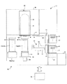
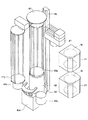
図1は、本実施の形態に係る成膜装置10を概略的に示す縦断面図である。図2は、ローディングエリア40を概略的に示す斜視図である。図3は、ボート44の一例を概略的に示す斜視図である。
FIG. 1 is a longitudinal sectional view schematically showing a
成膜装置10は、載置台(ロードポート)20、筐体30、及び制御部100を有する。
The
載置台(ロードポート)20は、筐体30の前部に設けられている。筐体30は、ローディングエリア(作業領域)40及び成膜容器60を有する。ローディングエリア40は、筐体30内の下方に設けられており、成膜容器60は、筐体30内であってローディングエリア40の上方に設けられている。また、ローディングエリア40と成膜容器60との間には、ベースプレート31が設けられている。なお、後述する供給機構70は、成膜容器60に接続されるように設けられている。
The mounting table (load port) 20 is provided in the front part of the
ベースプレート31は、成膜容器60の後述する反応管61を設置するための例えばSUS製のベースプレートであり、反応管61を下方から上方に挿入するための図示しない開口部が形成されている。
The
載置台(ロードポート)20は、筐体30内へのウェハWの搬入搬出を行うためのものである。載置台(ロードポート)20には、収納容器21、22が載置されている。収納容器21、22は、前面に図示しない蓋を着脱可能に備えた、複数枚例えば50枚程度のウェハWを所定の間隔で収納可能な密閉型収納容器(フープ)である。
The mounting table (load port) 20 is for carrying the wafer W into and out of the
また、載置台20の下方には、後述する移載機構47により移載されたウェハWの外周に設けられた切欠部(例えばノッチ)を一方向に揃えるための整列装置(アライナ)23が設けられていてもよい。
An alignment device (aligner) 23 for aligning notches (for example, notches) provided on the outer periphery of the wafer W transferred by the
ローディングエリア(作業領域)40は、収納容器21、22と後述するボート44との間でウェハWの移載を行い、ボート44を成膜容器60内に搬入(ロード)し、ボート44を成膜容器60から搬出(アンロード)するためのものである。ローディングエリア40には、ドア機構41、シャッター機構42、蓋体43、ボート44、基台45a、45b、昇降機構46、及び移載機構47が設けられている。
The loading area (working area) 40 transfers the wafer W between the
なお、蓋体43及びボート44は、本発明における基板保持部に相当する。
The
ドア機構41は、収納容器21、22の蓋を取外して収納容器21、22内をローディングエリア40内に連通開放するためのものである。
The
シャッター機構42は、ローディングエリア40の上方に設けられている。シャッター機構42は、蓋体43を開けているときに、後述する成膜容器60の開口63から高温の炉内の熱がローディングエリア40に放出されるのを抑制ないし防止するために開口63を覆う(又は塞ぐ)ように設けられている。
The
蓋体43は、保温筒48及び回転機構49を有する。保温筒48は、蓋体43上に設けられている。保温筒48は、ボート44が蓋体43側との伝熱により冷却されることを防止し、ボート44を保温するためのものである。回転機構49は、蓋体43の下部に取り付けられている。回転機構49は、ボート44を回転するためのものである。回転機構49の回転軸は蓋体43を気密に貫通し、蓋体43上に配置された図示しない回転テーブルを回転するように設けられている。
The
昇降機構46は、ボート44のローディングエリア40から成膜容器60に対する搬入、搬出に際し、蓋体43を昇降駆動する。そして、昇降機構46により上昇させられた蓋体43が成膜容器60内に搬入されているときに、蓋体43は、後述する開口63に当接して開口63を密閉するように設けられている。そして、蓋体43に載置されているボート44は、成膜容器60内でウェハWを水平面内で回転可能に保持することができる。
The elevating
なお、成膜装置10は、ボート44を複数有していてもよい。以下、本実施の形態では、図2を参照し、ボート44を2つ有する例について説明する。
The
ローディングエリア40には、ボート44a、44bが設けられている。そして、ローディングエリア40には、基台45a、45b及びボート搬送機構45cが設けられている。基台45a、45bは、それぞれボート44a、44bが蓋体43から移載される載置台である。ボート搬送機構45cは、ボート44a、44bを、蓋体43から基台45a、45bに移載するためのものである。
In the
ボート44a、44bは、例えば石英製であり、大口径例えば直径300mmのウェハWを水平状態で上下方向に所定の間隔(ピッチ幅)で搭載するようになっている。ボート44a、44bは、例えば図3に示すように、天板50と底板51の間に複数本例えば3本の支柱52を介設してなる。支柱52には、ウェハWを保持するための爪部53が設けられている。また、支柱52と共に補助柱54が適宜設けられていてもよい。
The
移載機構47は、収納容器21、22とボート44a、44bの間でウェハWの移載を行うためのものである。移載機構47は、基台57、昇降アーム58、及び、複数のフォーク(移載板)59を有する。基台57は、昇降及び旋回可能に設けられている。昇降アーム58は、ボールネジ等により上下方向に移動可能(昇降可能)に設けられ、基台57は、昇降アーム58に水平旋回可能に設けられている。
The
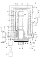
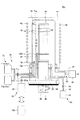
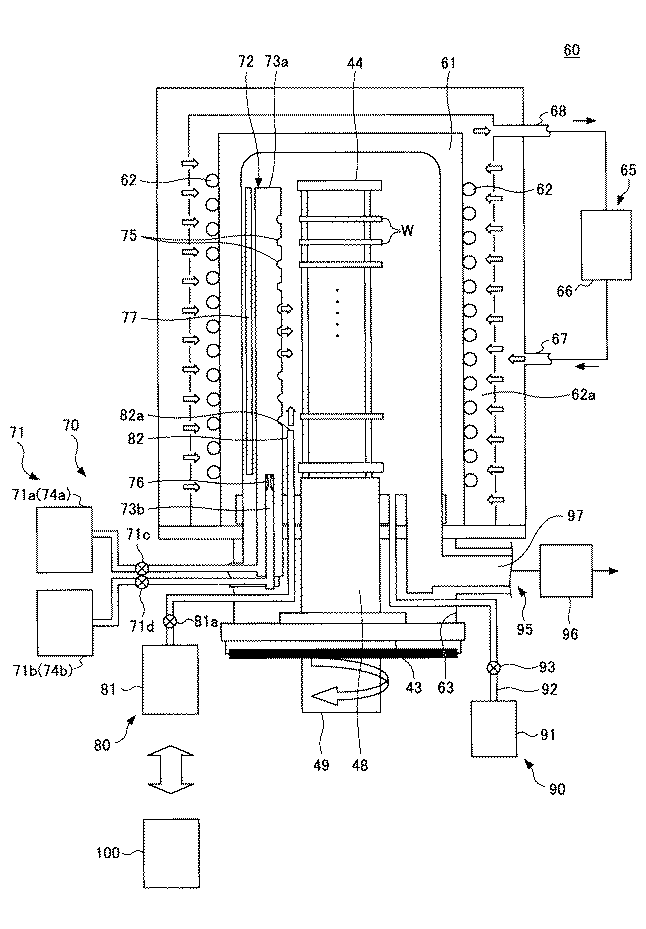
図4は、成膜容器60の構成の概略を示す断面図である。
FIG. 4 is a cross-sectional view schematically showing the configuration of the
成膜容器60は、例えば、複数枚の被処理基板例えば薄板円板状のウェハWを収容して所定の処理例えばCVD処理等を施すための縦型炉とすることができる。成膜容器60は、反応管61、ヒータ62、冷却機構65、供給機構70、密着促進剤供給機構80、パージガス供給機構90及び排気機構95を有する。
The
なお、ヒータ62は、本発明における加熱機構に相当する。
The
反応管61は、例えば石英製であり、縦長の形状を有しており、下端に開口63が形成されている。ヒータ(加熱装置)62は、反応管61の周囲を覆うように設けられており、反応管61内を所定の温度例えば50〜1200℃に加熱制御可能である。なお、反応管61内のウェハWの温度は、反応管61の周囲を覆うように設けられているヒータ62と、後述するインジェクタ72の近傍に設けられ、インジェクタ72の内部の温度を制御するインジェクタヒータ77とにより制御されてもよい。
The
図5は、冷却機構65の構成を模式的に示す図である。
FIG. 5 is a diagram schematically showing the configuration of the
冷却機構65は、送風機(ブロワ)66、送風管67、排気管68を有する。送風機(ブロワ)66は、ヒータ62が設けられている空間62a内に空気を送風して成膜容器60を冷却するためのものである。送風管67は、送風機66からの空気をヒータ62に送るためのものであり、空間62aに接続されている。排気管68は、ヒータ62内の空気を排出するためのものであり、空間62aに接続されている。
The
なお、空間62a内の空気は排気管68から熱交換器69を介して工場排気系に排出されるようになってもよい。あるいは、図5に示すように、熱交換器69を設け、工場排気系に排出せずに、熱交換器69での熱交換後に送風機66の吸引側に戻し、循環使用するようにしてもよい。また、その場合、エアフィルタ69aを介して循環させるとなおよい。エアフィルタ69aは、送風機66の吸い込み側に設けられていてもよいが、送風機66の吹き出し側に設けられている方がより好ましい。熱交換器69はヒータ62からの廃熱を利用するためのものでもある。
The air in the
このとき、成膜装置には、後述する制御部100の一部として、温度センサ101及び温度コントローラ102が設けられていてもよい。
At this time, the film forming apparatus may be provided with a
温度センサ101は、成膜容器60内の温度(ウェハWの温度)を検出するためのものである。温度コントローラ102は、温度センサ101が検出した検出温度をフィードバックさせながらヒータ62に供給する電力と送風機66に供給する電力とを制御するための制御装置である。温度コントローラ102には温度センサ101からの信号が入力されている。また、温度コントローラ102には、成膜容器60内の温度が効率よく設定温度(所定温度)に収束するように、ヒータ62に供給する電力と送風機66に供給する電力とを制御するためのプログラム(シーケンス)が組み込まれている。ヒータ62は、温度コントローラ102からの制御信号により、供給される電力が、電力コントローラ例えばサイリスタ103を介して制御される。また、送風機66は、温度コントローラ102からの信号により、供給される電力が、電力コントローラ例えばインバータ104を介して制御されるようになっている。
The
なお、インジェクタヒータ77が設けられているときは、温度コントローラ102は、温度センサ101が検出した検出温度をフィードバックさせながらヒータ62及びインジェクタヒータ77に供給する電力と送風機66に供給する電力とを制御する。また、温度コントローラ102には、成膜容器60内の温度が効率よく設定温度(所定温度)に収束するように、ヒータ62及びインジェクタヒータ77に供給する電力と送風機66に供給する電力とを制御するためのプログラム(シーケンス)が組み込まれている。インジェクタヒータ77も、温度コントローラ102からの制御信号により、供給される電力が、電力コントローラ例えばサイリスタ103を介して制御される。
When the
本実施の形態では、温度コントローラ102が、ウェハWの温度を、ウェハWにポリイミド膜を成膜するときの所定温度(成膜温度)まで上昇させる際に、温度センサ101からの信号を受け取り、受け取った信号に基づいて、ヒータ62に供給する電力と、冷却機構65に供給する電力とを制御する。そして、制御部100は、ヒータ62の加熱量と送風機66の冷却量とを制御する。これにより、成膜温度が例えば200℃程度の低温領域にあるときに、ウェハWの温度を上昇させる昇温過程において、成膜温度に収束させる収束時間、すなわち後述するリカバリ工程の所要時間を短縮化することができるとともに、収束した後、ウェハWの温度の安定性を向上させることができる。
In the present embodiment, the
供給機構70は、原料ガス供給部71、及び、成膜容器60内に設けられたインジェクタ72を含む。インジェクタ72は、供給管73aを含む。原料ガス供給部71は、インジェクタ72の供給管73aに接続されている。
The
本実施の形態では、供給機構70は、第1の原料ガス供給部71a及び第2の原料ガス供給部71bを有していてもよい。このとき、第1の原料ガス供給部71a及び第2の原料ガス供給部71bは、それぞれバルブ71c、71dを介し、インジェクタ72(供給管73a)に接続されている。第1の原料ガス供給部71aは、例えばPMDA原料を気化するための第1の気化器74aを有し、PMDAガスを供給することができる。また、第2の原料ガス供給部71bは、例えばODA原料を気化するための第2の気化器74bを有し、ODAガスを供給することができる。
In the present embodiment, the
供給管73aには成膜容器60内に開口する供給孔75が形成されている。インジェクタ72は、原料ガス供給部71から供給管73aを流れる第1の原料ガス及び第2の原料ガスを、供給孔75を介して成膜容器60内に供給する。
A
また、供給管73aは、上下方向に延在するように設けられていてもよい。そして、供給管73aには、複数の供給孔75が形成されていてもよい。なお、供給孔75の形状は、円形、楕円形、矩形等各種の形状であってもよい。
The
インジェクタ72は、内側供給管73bを含むことが好ましい。内側供給管73bは、供給管73aの供給孔75が形成されている部分よりも上流側の部分に収容されていてもよい。そして、内側供給管73bの下流側の端部付近には、供給管73aの内部空間に第1の原料ガス及び第2の原料ガスのいずれか一方の原料ガスを供給するための開口76が形成されていてもよい。このような構造を有する内側供給管73bを含むことによって、第1の原料ガスと第2の原料ガスとを供給孔75から成膜容器60内に供給する前に、予め供給管73aの内部空間において第1の原料ガスと第2の原料ガスとを十分混合させることができる。
The
なお、以下では、供給管73aに第1の原料ガスを供給し、内側供給管73bに第2の原料ガスを供給する場合を例示して、説明する。しかし、内側供給管73bに第1の原料ガスを供給し、供給管73aに第2の原料ガスを供給してもよい。
In the following, a case where the first source gas is supplied to the
また、開口76の形状は、円形、楕円形、矩形等各種の形状であってもよい。
The shape of the
本実施の形態は、ボート44が複数のウェハWを上下方向に所定の間隔で保持する例について説明するものである。このとき、供給管73aとともに、内側供給管73bも、上下方向に延在するように設けられていてもよい。更に、下方側を上流側、上方側を下流側とするときは、内側供給管73bは、供給管73aの供給孔75が形成されている部分よりも下方側の部分において、供給管73aの内部に収容されるように設けられていてもよい。そして、内側供給管73bの上端部付近には、供給管73aの内部空間と連通するための開口76が設けられていてもよい。
In the present embodiment, an example in which the
供給機構70は、例えば供給管73aに第1の原料ガスを流すとともに、内側供給管73bに第2の原料ガスを流す。そして、内側供給管73bを流れる第2の原料ガスを、開口76を介して供給管73aに合流させ、第1の原料ガスと第2の原料ガスとを混合させた状態で、供給孔75を介して成膜容器60内に供給する。
For example, the
また、供給管73aの近傍には、供給管73aの内部の温度を制御するインジェクタヒータ77が設けられていてもよい。また、前述したように、反応管61内のウェハWの温度は、インジェクタヒータ77とヒータ72とにより制御されてもよい。
An
図6は、密着促進剤供給機構80の構成を模式的に示す図である。なお、図6では、成膜容器60、ボート44及び密着促進剤供給機構80以外の図示を省略している。
FIG. 6 is a diagram schematically showing the configuration of the adhesion
図6に示すように、密着促進剤供給機構80は、密着促進剤供給部81及び成膜容器60内に設けられた供給管82を含む。密着促進剤供給部81は、バルブ81aを介し、供給管82に接続されている。密着促進剤供給機構80は、密着促進剤を気化させた密着促進剤ガスを成膜容器60内に供給し、ウェハWの表面を密着促進剤ガスにより処理するためのものである。
As shown in FIG. 6, the adhesion
密着促進剤供給部81は、保持容器83、ガス導入部84及びガス導出部85を有する。
The adhesion
保持容器83の内部には、例えばシランカップリング剤等の密着促進剤SCが充填可能に設けられている。保持容器83の内部には、加熱機構86が設けられており、保持容器83の内部に充填された密着促進剤SCを、加熱機構86により加熱して気化することができる。なお、加熱機構86としてヒータ等を用いることができる。また、保持容器83を加熱することができればよく、加熱機構86は、保持容器83の任意の場所に設けることができる。
In the holding
ガス導入部84は、保持容器83に、保持容器83で気化した密着促進剤ガスを搬送するための例えば窒素(N2)ガス等の不活性ガスよりなる密着促進剤キャリアガスを、密着促進剤キャリアガス供給部87から導入する。ガス導入部84は、ガス導入管84a及びガス導入口84bを有する。ガス導入管84aは、密着促進剤ガスを搬送する密着促進剤キャリアガスを保持容器83の外部から保持容器83の内部へ導入するための配管である。ガス導入管84aは、保持容器83の上面を貫通するように保持容器83の上面に取り付けられるとともに、保持容器83の内部を上方から下方に延在するように設けられている。また、ガス導入管84aは、一端が保持容器83の底部において開口するとともに、他端が保持容器83の外部で密着促進剤キャリアガス供給部87に接続されている。ガス導入口84bは、ガス導入管84aの下端に形成された開口である。
The
図6では、ガス導入口84bが密着促進剤SCの液面よりも下方にあり、ガス導入口84bから供給された密着促進剤キャリアガスが密着促進剤をバブリングする場合を例示している。しかし、ガス導入口84bは、密着促進剤SCの液面よりも上方にあってもよく、ガス導入口84bから供給された密着促進剤キャリアガスが密着促進剤SCをバブリングしなくてもよい。
FIG. 6 illustrates a case where the
ガス導出部85は、保持容器83から、密着促進剤キャリアガスとともに気化した密着促進剤ガスを導出する。ガス導出部85は、ガス導出管85a及びガス導出口85bを有する。ガス導出管85aは、密着促進剤ガスおよび密着促進剤キャリアガスを保持容器83の内部から保持容器83の外部へ導出するための配管である。ガス導出管85aは、保持容器83の上面を貫通するように保持容器83の上面に取り付けられている。また、ガス導出管85aは、一端が保持容器83の内部上方で開口されるように設けられており、他端が成膜容器60の内部に設けられた供給管82に接続されている。ガス導出口85bは、ガス導出管85aの下端に形成された開口である。
The
供給管82は、反応管61の側壁を内側へ貫通して上方向へ屈曲されて延びる石英管よりなる。供給管82の先端には、成膜容器60内に開口する供給孔82aが形成されている。供給管82は、密着促進剤供給部81から供給管82を流れる気化した密着促進剤ガスを、供給孔82aを介して成膜容器60内に供給する。供給孔82aは、ボート44に搭載されたウェハWの近傍に、1箇所設けられているのが好ましい。これにより、供給孔82aより吐出された密着促進剤ガスを、成膜容器60内に一様に拡散させることができる。
The
パージガス供給機構90は、パージガス供給部91、及びパージガス供給管92を含む。パージガス供給部91は、パージガス供給管92を介して成膜容器60に接続されており、成膜容器60内にパージガスを供給する。また、パージガス供給管92の途中には、パージガス供給部91と成膜容器60の内部とを連通又は遮断するためのバルブ93が設けられている。
The purge
排気機構95は、排気装置96及び排気管97を含む。排気機構95は、成膜容器60内から排気管97を介してガスを排気するためのものである。
The
制御部100は、例えば、図示しない演算処理部、記憶部及び表示部を有する。演算処理部は、例えばCPU(Central Processing Unit)を有するコンピュータである。記憶部は、演算処理部に、各種の処理を実行させるためのプログラムを記録した、例えばハードディスクにより構成されるコンピュータ読み取り可能な記録媒体である。表示部は、例えばコンピュータの画面よりなる。演算処理部は、記憶部に記録されたプログラムを読み取り、そのプログラムに従って、ボート44(基板保持部)、ヒータ62、冷却機構65、供給機構70、密着促進剤供給機構80、パージガス供給機構90、及び、排気機構95を構成する各部に制御信号を送り、後述するような成膜処理を実行する。
The
また、前述したように、制御部100は、温度センサ101、温度コントローラ102、サイリスタ103及びインバータ104を有していてもよい。
Further, as described above, the
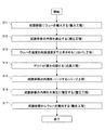
次に、本実施の形態に係る成膜装置を用いた成膜処理について説明する。図7は、本実施の形態に係る成膜装置を用いた成膜処理における各工程の手順を説明するためのフローチャートである。 Next, a film forming process using the film forming apparatus according to this embodiment will be described. FIG. 7 is a flowchart for explaining the procedure of each step in the film forming process using the film forming apparatus according to the present embodiment.
実施の形態(実施例)では、成膜処理開始後、ステップS11として、成膜容器60内にウェハWを搬入する(搬入工程)。図1に示した成膜装置10の例では、例えばローディングエリア40において、移載機構47により収納容器21からボート44aへウェハWを搭載し、ウェハWを搭載したボート44aをボート搬送機構45cにより蓋体43に載置することができる。そして、ボート44aを載置した蓋体43を昇降機構46により上昇させて成膜容器60内に挿入することにより、ウェハWを搬入することができる。
In the embodiment (example), after starting the film forming process, the wafer W is loaded into the
次に、ステップS12では、成膜容器60の内部を減圧する(減圧工程)。排気装置96の排気能力又は排気装置96と排気管97との間に設けられている図示しない流量調整バルブを調整することにより、排気管97を介して成膜容器60を排気する排気量を増大させる。そして、成膜容器60の内部を所定圧力例えば大気圧(760Torr)から例えば0.3Torrに減圧する。
Next, in step S12, the inside of the
次に、ステップS13では、ウェハWの温度を、ウェハWにポリイミド膜を成膜するときの所定温度(成膜温度)まで上昇させる(リカバリ工程)。 Next, in step S13, the temperature of the wafer W is raised to a predetermined temperature (deposition temperature) when a polyimide film is formed on the wafer W (recovery step).
ボート44aを成膜容器60の内部に搬入した直後は、成膜容器60に設けられた温度センサ101の温度は、室温に近いため、ヒータ62に電力を供給することによって、ボート44aに搭載されているウェハWの温度を成膜温度まで上昇させる。
Immediately after the
本実施の形態では、ヒータ62と冷却機構65とにより、ウェハWの温度が成膜温度に収束するように、制御する。例えば、送風機66の風量(冷却量)を一定に保った状態で、ヒータ62に供給する電力(加熱量)を制御することができる(第1の制御方法)。第1の制御方法では、送風機66の風量を一定にした状態で、ウェハWの温度が成膜温度に到達する直前まで、ヒータ62に供給する電力を増加させる。そして、ウェハWの温度が成膜温度に安定する直前に、ヒータ62に供給する電力を減少させ、ウェハWの温度を所定の温度に収束させる。これにより、ウェハWの温度を成膜温度に収束する収束時間を短縮することができるとともに、成膜温度に収束した後、ウェハWの温度を安定に制御することができる。
In the present embodiment, control is performed by the
あるいは、ウェハWの温度が成膜温度に到達する直前に、ヒータ62に供給する電力を減少させるとともに、送風機66の風量を増加させて成膜容器60を強制的に冷却し、ウェハWの温度を成膜温度に収束させてもよい(第2の制御方法)。
Alternatively, immediately before the temperature of the wafer W reaches the film formation temperature, the power supplied to the
図8は、ヒータ62と冷却機構65を制御する制御方法の一例(第2の制御方法)を説明するための図である。図8(a)は、ウェハWの温度の時間依存性を、冷却機構65を用いて本実施の形態(実施例)に係る制御方法(第2の制御方法)を行った場合と、冷却機構65を用いない場合(比較例1)とで比較して示すグラフである。また、図8(b)は、本実施の形態(実施例)における、ヒータ62の加熱量と送風機66の冷却量の時間依存性と示すグラフである。
FIG. 8 is a diagram for explaining an example of a control method (second control method) for controlling the
第2の制御方法では、ウェハWの温度が成膜温度に到達する直前に、ヒータ62に供給する電力(加熱量)を0に減少させるのと同時に、送風機66の風量(冷却量)を増加させる。これにより、図8(a)に示すように、ウェハWの温度を成膜温度に収束する収束時間を、比較例1に比べ、時間T1短縮することができる。
In the second control method, immediately before the temperature of the wafer W reaches the film formation temperature, the power (heating amount) supplied to the
更に、本実施の形態では、リカバリ工程において、ウェハWの表面を密着促進剤により処理する。すなわち、ヒータ62によりウェハWを加熱するとともに、密着促進剤供給機構80により成膜容器60内に密着促進剤ガスを供給し、供給された密着促進剤ガスによりウェハWの表面を処理する。
Furthermore, in the present embodiment, the surface of the wafer W is treated with an adhesion promoter in the recovery process. That is, the wafer W is heated by the
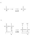
図9は、密着促進剤としてシランカップリング剤を用いたときのウェハWの表面における反応を示す図である。図10及び図11は、比較例2としてシランカップリング剤及び水蒸気を用いたときのウェハWの表面における反応を示す図である。 FIG. 9 is a diagram showing a reaction on the surface of the wafer W when a silane coupling agent is used as the adhesion promoter. 10 and 11 are diagrams showing the reaction on the surface of the wafer W when a silane coupling agent and water vapor are used as Comparative Example 2. FIG.
シランカップリング剤として、分子中に例えばアルコキシ基(RO−(R;アルキル基))を有するオルガノシランを用いることが好ましい。図9では、分子中に例えばメトキシ基(CH3O−)を有するオルガノシランを用いた例を示す。そして、図9(a)に示すように、表面が水酸基すなわちヒドロキシ基(−OH)で終端されたSiウェハを用いるときは、シランカップリング剤のメトキシ基が、ウェハ表面のヒドロキシ基と熱反応してメタノール(CH3OH)が生成することによって、ウェハ表面に吸着する。また、図9(b)に示すように、表面が水素原子(H)で終端されたSiウェハを用いるときは、シランカップリング剤のメトキシ基が、ウェハ表面の水素原子と熱反応してメタン(CH4)が生成することによって、ウェハ表面に吸着する。 As the silane coupling agent, for example, organosilane having an alkoxy group (RO- (R; alkyl group)) in the molecule is preferably used. FIG. 9 shows an example using an organosilane having, for example, a methoxy group (CH 3 O—) in the molecule. Then, as shown in FIG. 9A, when using a Si wafer whose surface is terminated with a hydroxyl group, that is, a hydroxy group (—OH), the methoxy group of the silane coupling agent reacts with the hydroxyl group on the wafer surface in a thermal reaction. Then, methanol (CH 3 OH) is generated and adsorbed on the wafer surface. As shown in FIG. 9B, when a Si wafer having a surface terminated with hydrogen atoms (H) is used, the methoxy group of the silane coupling agent reacts with the hydrogen atoms on the wafer surface to react with methane. When (CH 4 ) is generated, it is adsorbed on the wafer surface.
一方、比較例2として、分子中に例えばアルコキシ基を有するシランカップリング剤と、水蒸気とを用いた場合を考える。すると、図10(a)に示すように、シランカップリング剤のアルコキシ基が、雰囲気中の水蒸気により加水分解することによって、水酸基すなわちヒドロキシ基(−OH)になる。そして、ウェハWとして、表面がヒドロキシ基(−OH)で終端されたSiウェハを用いるときは、図10(b)に示すように、シランカップリング剤のアルコキシ基が、ウェハ表面のヒドロキシ基と脱水縮合することによって、ウェハ表面に吸着する。 On the other hand, as Comparative Example 2, a case where a silane coupling agent having, for example, an alkoxy group in the molecule and water vapor are used will be considered. Then, as shown to Fig.10 (a), the alkoxy group of a silane coupling agent hydrolyzes with the water vapor | steam in atmosphere, It becomes a hydroxyl group, ie, a hydroxy group (-OH). When a Si wafer whose surface is terminated with a hydroxy group (—OH) is used as the wafer W, as shown in FIG. 10B, the alkoxy group of the silane coupling agent is different from the hydroxy group on the wafer surface. It is adsorbed on the wafer surface by dehydration condensation.
あるいは、図11に示すように、シランカップリング剤のアルコキシ基が水蒸気により加水分解してヒドロキシ基になり、更に重合反応してオリゴマー化することがある。また、オリゴマー化したシランカップリング剤は、表面がヒドロキシ基(−OH)で終端されたSiウェハに近づくと、中間体を経て、更に加熱脱水することによって、ウェハ表面に吸着することがある。このように、比較例2では、シランカップリング剤が重合することによって、パーティクルが発生するおそれがある。 Alternatively, as shown in FIG. 11, the alkoxy group of the silane coupling agent may be hydrolyzed with water vapor to become a hydroxy group, and further polymerized to be oligomerized. Further, when the oligomerized silane coupling agent approaches the Si wafer terminated with a hydroxy group (—OH), the oligomerized silane coupling agent may be adsorbed on the wafer surface by further heating and dehydrating through an intermediate. Thus, in Comparative Example 2, particles may be generated due to polymerization of the silane coupling agent.
一方、本実施の形態では、シランカップリング剤が重合しないため、パーティクルの発生を防止できる。 On the other hand, in this Embodiment, since a silane coupling agent does not superpose | polymerize, generation | occurrence | production of a particle can be prevented.
また、比較例2では、水蒸気を用いるため、後述する成膜工程以降において、成膜容器内に残留する水蒸気によって、下記式(1) Moreover, in Comparative Example 2, since water vapor is used, the water vapor remaining in the film formation container after the film formation step described later is used to reduce the following formula (1).
また、比較例2では、表面がヒドロキシ基で終端されたSiウェハを用いるため、図12に示すように、予めSiウェハよりなるウェハWをDHF(希フッ酸)洗浄して表面を水素原子で終端した後、SC1(アンモニア過水)洗浄して表面をヒドロキシ基で終端しなければならない。そのため、ウェハ表面の終端状態を調整する工程数が多い。一方、本実施の形態では、表面がヒドロキシ基で終端されたウェハW、及び、表面が水素原子で終端されたウェハWのいずれを用いてもよい。そのため、ウェハ表面の終端状態を調整する工程数を削減できる。 Further, in Comparative Example 2, since the Si wafer whose surface is terminated with a hydroxy group is used, as shown in FIG. 12, the wafer W made of Si wafer is previously washed with DHF (dilute hydrofluoric acid) and the surface is made of hydrogen atoms. After termination, the surface must be terminated with hydroxy groups by SC1 (ammonia peroxide) cleaning. Therefore, the number of processes for adjusting the termination state of the wafer surface is large. On the other hand, in this embodiment, either a wafer W whose surface is terminated with a hydroxy group or a wafer W whose surface is terminated with a hydrogen atom may be used. Therefore, the number of steps for adjusting the termination state of the wafer surface can be reduced.
また、比較例3に係る成膜処理として、密着促進剤ガスによる表面処理を、成膜装置と別に設けられた表面処理装置を用いて行う場合を考える。 Further, as a film forming process according to Comparative Example 3, a case is considered in which a surface treatment using an adhesion promoter gas is performed using a surface treatment apparatus provided separately from the film forming apparatus.
図13は、本実施の形態に係る成膜処理を実施例とし、実施例に係る成膜処理と比較例3に係る成膜処理とを比較して示すタイムチャートである。比較例3に係る成膜処理では、搬入工程(ステップS11)の前に、成膜容器60と別に設けられた例えば表面処理装置により、ウェハWの表面処理工程(ステップS10)を行わなければならない。従って、図13の右側に示す実施の形態(実施例)に係る成膜処理は、図13の左側に示す比較例3に係る成膜処理に比べ、成膜容器60と別に設けられた表面処理装置により表面処理工程を行う時間T2の分だけ処理時間を短縮することができる。その結果、単位時間当たりに成膜処理されるウェハの枚数を増やすことができる。
FIG. 13 is a time chart showing the film forming process according to the present embodiment as an example and comparing the film forming process according to the example with the film forming process according to comparative example 3. In the film forming process according to the comparative example 3, the surface processing process (step S10) of the wafer W must be performed by, for example, a surface processing apparatus provided separately from the
次に、ステップS14では、ポリイミド膜を成膜する(成膜工程)。 Next, in step S14, a polyimide film is formed (film formation process).
制御部100により、供給管73aに第1の原料ガスを流す第1の流量F1と、内側供給管73bに第2の原料ガスを流す第2の流量F2とを予め設定しておく。そして、回転機構49によりウェハWを回転させた状態で、設定した第1の流量F1で第1の原料ガス供給部71aから第1の原料ガスを供給管73aに流し、設定した第2の流量F2で第2の原料ガス供給部71bから第2の原料ガスを内側供給管73bに流すことによって、第1の原料ガスと第2の原料ガスとを所定の混合比で混合させた状態で成膜容器60内に供給する。そして、ウェハWの表面でPMDAとODAを重合反応させ、ポリイミド膜を成膜する。具体的には、例えば第1の流量F1を900sccmとし、第2の流量F2を900sccmとすることができる。
The
このときの、PMDAとODAとの重合反応は、次の式(2)に従う。 The polymerization reaction between PMDA and ODA at this time follows the following formula (2).
また、ウェハWの表面全面が密着促進剤により処理されていないと、原料ガスがウェハWの表面に到達しても、成膜速度が異なることがある。本実施の形態(実施例)では、成膜工程の直前のリカバリ工程において、ウェハWの表面全面を密着促進剤により均一に処理することができる。これにより、ウェハWの全面において成膜速度を均一にすることができ、ウェハWの面内における膜厚を均一にすることができる。 Further, if the entire surface of the wafer W is not treated with the adhesion promoter, the film formation rate may be different even if the source gas reaches the surface of the wafer W. In the present embodiment (example), the entire surface of the wafer W can be uniformly treated with the adhesion promoter in the recovery step immediately before the film forming step. Thereby, the film formation rate can be made uniform over the entire surface of the wafer W, and the film thickness in the surface of the wafer W can be made uniform.
比較例3に係る成膜処理を行ったとき、すなわち密着促進剤ガスによる表面処理を、成膜容器60と別の表面処理装置により行ったとき、成膜されたポリイミド膜の膜厚の面内均一性(1σ)は、3.5%であった。一方、実施の形態(実施例)に係る成膜処理を行ったとき、すなわち、密着促進剤ガスによる表面処理を、成膜容器60内で行ったとき、成膜されたポリイミド膜の膜厚の面内均一性(1σ)は、2.1%であった。このように、本実施の形態により、ウェハWの面内における膜厚を均一にすることができる。
When the film formation process according to Comparative Example 3 is performed, that is, when the surface treatment with the adhesion promoter gas is performed by a surface treatment apparatus different from the
次に、ステップS15では、第1の原料ガス供給部71aからのPMDAガスの供給及び第2の原料ガス供給部71bからのODAガスの供給を停止し、成膜容器60の内部をパージガスによりパージする(パージ工程)。
Next, in step S15, the supply of PMDA gas from the first source
バルブ71cを閉じ、第1の原料ガス供給部71aからの第1の原料ガスの供給を停止する。また、バルブ71dを閉じ、第2の原料ガス供給部71bからの第2の原料ガスの供給を停止する。そして、パージガス供給機構90と排気機構95とを制御することにより、成膜容器60の内部の原料ガスをパージガスに置換する。
The
例えば、排気装置96の排気能力又は排気装置96と排気管97との間に設けられている図示しない流量調整バルブを調整して排気量を増やすことにより、成膜容器60の内部を例えば0.3Torrに減圧する。その後、排気量を減少させるか、又は排気量を0にして排気を停止した状態で、成膜容器60内の内部の圧力が例えば5.0Torrになるまで、バルブ93を開いてパージガス供給機構90によりパージガスを成膜容器60内に供給する。これにより、成膜容器60内の原料ガスをパージガスに置換できる。また、排気機構95による減圧と、パージガス供給機構90によるパージガスの供給とを1回行った後、更に減圧とパージガスの供給を複数回繰り返してもよい。これにより、成膜容器60内の原料ガスを、更に確実にパージガスに置換できる。
For example, by adjusting the exhaust capacity of the
本実施の形態では、パージ工程において、ウェハ上に成膜されたポリイミド膜をヒータにより熱処理してもよい。熱処理は、成膜後、膜中のイミド化していない部分をイミド化するために行う。ポリイミドは高い絶縁性を有するため、膜中のポリイミドの割合であるイミド化率を上昇させることによって、成膜したポリイミド膜の絶縁性を向上させることができる。 In the present embodiment, the polyimide film formed on the wafer may be heat-treated with a heater in the purge process. The heat treatment is carried out after the film formation in order to imidize a portion of the film that has not been imidized. Since polyimide has high insulating properties, it is possible to improve the insulating properties of the formed polyimide film by increasing the imidization ratio, which is the ratio of the polyimide in the film.
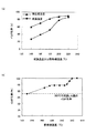
図14は、ポリイミド膜のイミド化率の成膜温度依存性及び熱処理温度依存性を示すグラフである。図14(a)は、イミド化率の成膜温度依存性及び熱処理温度依存性を示す。図14(b)は、イミド化率の熱処理温度依存性を示す。図14におけるイミド化率は、成膜後のポリイミド膜をFT−IR法により分析して得たデータである。 FIG. 14 is a graph showing the film formation temperature dependency and the heat treatment temperature dependency of the imidization ratio of the polyimide film. FIG. 14A shows the film formation temperature dependence and heat treatment temperature dependence of the imidization rate. FIG. 14B shows the heat treatment temperature dependence of the imidization rate. The imidation ratio in FIG. 14 is data obtained by analyzing the polyimide film after film formation by the FT-IR method.
図14(a)に示すように、成膜温度が200℃未満であって、熱処理温度が200℃未満の場合、イミド化率が低下する。従って、成膜温度及び熱処理温度は、200℃以上であることが好ましい。これにより、絶縁性に優れたポリイミド膜を得ることができる。 As shown in FIG. 14 (a), when the film formation temperature is less than 200 ° C. and the heat treatment temperature is less than 200 ° C., the imidization rate decreases. Accordingly, the film formation temperature and the heat treatment temperature are preferably 200 ° C. or higher. Thereby, the polyimide film excellent in insulation can be obtained.
また、図14(b)に示すように、熱処理温度が200〜300℃では、熱処理温度の増加に伴って、イミド化率が上昇する。熱処理温度が300〜350℃では、350℃付近にあるガラス遷移温度の影響を受け、イミド化率はほとんど変化しない。熱処理温度が350〜380℃では、熱処理温度の増加に伴って、イミド化率が急激に上昇し、380℃でイミド化率が略100%に達する。従って、380℃以上の温度、例えば400℃以上の温度で熱処理を行うことがより好ましい。これにより、ポリイミド膜を略完全にイミド化することができ、更に絶縁性に優れたポリイミド膜を得ることができる。 Moreover, as shown in FIG.14 (b), when the heat processing temperature is 200-300 degreeC, the imidation rate rises with the increase in heat processing temperature. When the heat treatment temperature is 300 to 350 ° C., the imidization rate hardly changes under the influence of the glass transition temperature in the vicinity of 350 ° C. When the heat treatment temperature is 350 to 380 ° C., the imidization rate rapidly increases as the heat treatment temperature increases, and at 380 ° C., the imidization rate reaches approximately 100%. Therefore, it is more preferable to perform the heat treatment at a temperature of 380 ° C. or higher, for example, 400 ° C. or higher. Thereby, a polyimide film can be imidized almost completely and a polyimide film excellent in insulation can be obtained.
また、200℃の成膜温度で成膜したポリイミド膜を200℃の熱処理温度で熱処理する際の熱処理時間を10分、20分、40分、70分と変えた場合における、リーク電流及びイミド化率を調べた結果を表1に示す。表1では、1.0MV/cmの電界を印加したときのリーク電流を示す。 In addition, the leakage current and imidization when the heat treatment time when the polyimide film formed at the film formation temperature of 200 ° C. is heat-treated at the heat treatment temperature of 200 ° C. is changed to 10 minutes, 20 minutes, 40 minutes, and 70 minutes. The results of examining the rates are shown in Table 1. Table 1 shows the leakage current when an electric field of 1.0 MV / cm is applied.
また、パージ工程における熱処理を行う際も、ヒータ62と冷却機構65とを制御することによって、ウェハ温度を制御することが好ましい。
Also, when performing the heat treatment in the purge process, it is preferable to control the wafer temperature by controlling the
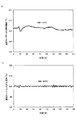
図15は、ボート44aを成膜容器60内に搬入した時から搬出する時までの間の成膜容器60に設けられた温度センサ101の測定結果の一例を、冷却機構65を用いた場合と冷却機構65を用いない場合との間で比較して示すグラフである。図15(a)は、冷却機構65を用いていない場合を示し、図15(b)は、冷却機構65を用いた場合を示す。
FIG. 15 shows a case where the
図15(a)に示すように、冷却機構65を用いていないとき、目標温度を200℃とすると、温度センサが測定する温度は目標温度を中心に±4.0℃の範囲で変動する。一方、図15(b)に示すように、冷却機構65を用いたときは、温度センサが測定する温度は目標温度を中心に±0.5℃の範囲でしか変動しない。従って、ヒータ62と冷却機構65とを制御することによって、200℃の温度領域でも、高精度で温度を制御できる。
As shown in FIG. 15A, when the
また、前述した比較例3に係る成膜処理として、イミド化のための熱処理を、成膜装置と別に設けられた熱処理装置を用いて行うものとする。すると、比較例3では、一連の成膜処理の後、すなわち搬出工程(ステップS17)の後、改めて成膜容器60により、又は、成膜容器60と別に設けられた熱処理装置により、イミド化のための熱処理工程(ステップS18)を行わなければならない。従って、図13の右側に示す実施の形態(実施例)に係る成膜処理は、図13の左側に示す比較例3に係る成膜処理に比べ、成膜容器60と別に設けられた熱処理装置により熱処理工程を行う時間T3の分だけ処理時間を短縮することができる。その結果、単位時間当たりに成膜処理されるウェハの枚数を増やすことができる。
In addition, as the film formation process according to Comparative Example 3 described above, heat treatment for imidization is performed using a heat treatment apparatus provided separately from the film formation apparatus. Then, in Comparative Example 3, after a series of film forming processes, that is, after the unloading step (step S17), imidization is performed again by the
次に、ステップS16では、成膜容器60の内部を大気圧に復圧する(復圧工程)。排気装置96の排気能力又は排気装置96と排気管97との間に設けられている図示しない流量調整バルブを調整することにより、成膜容器60を排気する排気量を減少させ、成膜容器60の内部を例えば0.3Torrから例えば大気圧(760Torr)に復圧する。
Next, in step S16, the inside of the
なお、ポリイミド膜の熱処理は、ポリイミド膜を成膜した後、後述する搬出工程の前に、成膜容器の内部で行えばよく、復圧工程の際、又は、復圧工程の後に行ってもよい。 In addition, the heat treatment of the polyimide film may be performed inside the film formation container after the polyimide film is formed and before the unloading process described later, and may be performed during the decompression process or after the decompression process. Good.
次に、ステップS17では、成膜容器60からウェハWを搬出する(搬出工程)。図1に示した成膜装置10の例では、例えばボート44aを載置した蓋体43を昇降機構46により下降させて成膜容器60内からローディングエリア40に搬出することができる。そして、移載機構47により、搬出した蓋体43に載置されているボート44aから収納容器21へウェハWを移載することによって、ウェハWを成膜容器60から搬出することができる。その後、成膜処理を終了する。
Next, in step S17, the wafer W is unloaded from the film forming container 60 (unloading step). In the example of the
なお、複数のバッチについて連続して成膜処理を行うときは、更に、ローディングエリア40において、移載機構47により収納容器21からウェハWをボート44へ移載し、再びステップS11に戻り、次のバッチの成膜処理を行う。
(第1の実施の形態の変形例)
次に、図16を参照し、本発明の第1の実施の形態の変形例に係る成膜装置について説明する。
In addition, when the film forming process is continuously performed for a plurality of batches, the wafer W is transferred from the
(Modification of the first embodiment)
Next, a film forming apparatus according to a modification of the first embodiment of the present invention will be described with reference to FIG.
本変形例に係る成膜装置は、基板の表面を密着促進剤により処理した後、ポリイミド膜を成膜する前に、第1の原料ガスにより処理する点で、第1の実施の形態に係る成膜装置と相違する。なお、本変形例に係る成膜装置として、第1の実施の形態に係る成膜装置と同一の成膜装置を用いることができ、成膜装置についての説明を省略する。 The film forming apparatus according to this modification relates to the first embodiment in that the substrate surface is treated with the adhesion promoter and then treated with the first source gas before the polyimide film is formed. It is different from the film forming apparatus. As the film forming apparatus according to this modification, the same film forming apparatus as the film forming apparatus according to the first embodiment can be used, and the description of the film forming apparatus is omitted.
図16は、本変形例に係る成膜装置を用いた成膜処理における各工程の手順を説明するためのフローチャートである。 FIG. 16 is a flowchart for explaining the procedure of each step in the film forming process using the film forming apparatus according to this modification.
本変形例では、リカバリ工程(ステップS13)の後、成膜工程(ステップS14)の前に、第1の原料ガス供給部71aにより第1の原料ガスを供給し、ウェハ表面を第1の原料ガスにより処理する(第1の原料ガス供給工程(ステップS13−2))。
In this modification, after the recovery process (step S13) and before the film formation process (step S14), the first source gas is supplied by the first source
例えば、第1の実施の形態において、成膜したポリイミド膜の膜厚の面内均一性(1σ)が14.3%であるようなプロセス条件と同じ条件であって、第1の原料ガス供給工程を追加した場合、面内均一性(1σ)を2.3%まで低減できた。これは、例えば、シランカップリング剤のSiウェハに吸着している側と反対側の官能基とPMDAとが反応し、ウェハ表面の全面にPMDAが吸着した状態になったためと考えられる。そのため、成膜工程において、ウェハ表面の全面にポリイミド膜を均一に成膜することができる。
(第2の実施の形態)
次に、図17を参照し、本発明の第2の実施の形態に係る成膜装置について説明する。
For example, in the first embodiment, the first raw material gas supply is the same as the process condition in which the in-plane uniformity (1σ) of the film thickness of the formed polyimide film is 14.3%. When the process was added, the in-plane uniformity (1σ) could be reduced to 2.3%. This is considered to be because, for example, the functional group on the side opposite to the side adsorbed on the Si wafer of the silane coupling agent reacts with PMDA, and PMDA is adsorbed on the entire surface of the wafer. Therefore, in the film forming process, the polyimide film can be uniformly formed on the entire surface of the wafer surface.
(Second Embodiment)
Next, a film forming apparatus according to a second embodiment of the present invention will be described with reference to FIG.
本実施の形態に係る成膜装置は、成膜容器が冷却機構を有していない点で、第1の実施の形態に係る成膜装置と相違する。なお、本実施の形態に係る成膜装置は、成膜容器60a以外の部分は、第1の実施の形態に係る成膜装置と同一であり、成膜容器60a以外の部分についての説明を省略する。
The film forming apparatus according to the present embodiment is different from the film forming apparatus according to the first embodiment in that the film forming container does not have a cooling mechanism. The film forming apparatus according to the present embodiment is the same as the film forming apparatus according to the first embodiment except for the
図17は、成膜容器60aの構成の概略を示す断面図である。第1の実施の形態と同様に、成膜容器60aは、例えば、複数枚の被処理基板例えば薄板円板状のウェハWを収容して所定の処理例えばCVD処理等を施すための縦型炉とすることができる。また、成膜容器60aは、反応管61、ヒータ62、供給機構70、密着促進剤供給機構80、パージガス供給機構90及び排気機構95を有する。反応管61、ヒータ62、供給機構70、密着促進剤供給機構80、パージガス供給機構90及び排気機構95については、それぞれ第1の実施の形態における反応管61、ヒータ62、密着促進剤供給機構80、パージガス供給機構90及び排気機構95と同一の構成とすることができる。ただし、成膜容器60aは、冷却機構を有していない。
FIG. 17 is a cross-sectional view schematically illustrating the configuration of the
本実施の形態に係る成膜装置による成膜処理でも、第1の実施の形態と同様に、リカバリ工程において、密着促進剤供給機構により密着促進剤を供給し、表面処理を行うことができる。これにより、成膜されたポリイミド膜の膜質を向上させるとともに、単位時間当たりに成膜処理されるウェハの枚数を増やすことができる。 Also in the film forming process by the film forming apparatus according to the present embodiment, the surface treatment can be performed by supplying the adhesion promoter by the adhesion promoter supply mechanism in the recovery process, as in the first embodiment. As a result, the film quality of the formed polyimide film can be improved and the number of wafers to be processed per unit time can be increased.
また、本実施の形態に係る成膜装置による成膜処理でも、第1の実施の形態と同様に、パージ工程において、成膜されたポリイミド膜の熱処理を行うことができる。これにより、成膜されたポリイミド膜の膜質を向上させるとともに、単位時間当たりに成膜処理されるウェハの枚数を増やすことができる。 Also, in the film forming process by the film forming apparatus according to the present embodiment, as in the first embodiment, the formed polyimide film can be heat-treated in the purge process. As a result, the film quality of the formed polyimide film can be improved and the number of wafers to be processed per unit time can be increased.
以上、本発明の好ましい実施の形態について記述したが、本発明はかかる特定の実施の形態に限定されるものではなく、特許請求の範囲内に記載された本発明の要旨の範囲内において、種々の変形・変更が可能である。 The preferred embodiments of the present invention have been described above, but the present invention is not limited to such specific embodiments, and various modifications can be made within the scope of the gist of the present invention described in the claims. Can be modified or changed.
10 成膜装置
43 蓋体(基板保持部)
44、44a、44b ボート(基板保持部)
60 成膜容器
65 冷却機構
70 供給機構
71 原料ガス供給部
80 密着促進剤供給機構
90 パージガス供給機構
95 排気機構
100 制御部
W ウェハ
10
44, 44a, 44b Boat (substrate holding part)
60
Claims (7)
前記成膜容器内に搬入されている基板を加熱する加熱機構と、
前記成膜容器内に密着促進剤を気化させた密着促進剤ガスを供給する密着促進剤供給機構と、
前記加熱機構と前記密着促進剤供給機構とを制御する制御部と
を有し、
前記制御部は、基板を前記成膜容器内に搬入した後、前記加熱機構により、前記基板の温度を、前記基板にポリイミド膜を成膜するときの所定温度まで上昇させる間に、前記密着促進剤供給機構により前記密着促進剤ガスを前記成膜容器内に供給し、前記基板の表面を前記密着促進剤ガスにより処理するように、制御するものである、成膜装置。 A substrate in which a first raw material gas obtained by vaporizing a first raw material made of acid dianhydride and a second raw material gas obtained by vaporizing a second raw material made of diamine are carried into a film formation container. In a film forming apparatus for forming a polyimide film on the substrate by supplying to
A heating mechanism for heating the substrate carried into the film formation container;
An adhesion promoter supply mechanism for supplying an adhesion promoter gas obtained by vaporizing the adhesion promoter in the film formation container;
A controller that controls the heating mechanism and the adhesion promoter supply mechanism;
After the controller carries the substrate into the film formation container, the heating mechanism raises the adhesion while the temperature of the substrate is raised to a predetermined temperature when the polyimide film is formed on the substrate. A film forming apparatus for controlling the surface of the substrate to be treated with the adhesion promoter gas by supplying the adhesion promoter gas into the film formation container by an agent supply mechanism.
前記供給孔は、前記基板保持部に保持されている基板の近傍に配置されている、請求項2に記載の成膜装置。 A substrate holding unit for holding the substrate in the film formation container;
The film forming apparatus according to claim 2, wherein the supply hole is disposed in the vicinity of the substrate held by the substrate holding unit.
前記制御部は、前記基板の表面を前記密着促進剤ガスにより処理した後、前記基板にポリイミド膜を成膜する前に、前記第1の原料ガス供給部により前記第1の原料ガスを供給し、前記基板の表面を前記第1の原料ガスにより処理するように、制御するものである、請求項1から請求項3のいずれかに記載の成膜装置。 A first source gas supply unit configured to supply the first source gas into the film formation container;
The control unit supplies the first source gas from the first source gas supply unit after the surface of the substrate is treated with the adhesion promoter gas and before forming a polyimide film on the substrate. The film forming apparatus according to claim 1, wherein the surface of the substrate is controlled so as to be treated with the first source gas.
前記制御部は、前記基板の温度を前記所定温度まで上昇させる際に、前記加熱機構の加熱量と前記冷却機構の冷却量とを制御するものである、請求項1から請求項4のいずれかに記載の成膜装置。 A cooling mechanism for cooling the film formation container by blowing air to the film formation container;
5. The control unit according to claim 1, wherein the controller controls a heating amount of the heating mechanism and a cooling amount of the cooling mechanism when the temperature of the substrate is raised to the predetermined temperature. 6. 2. The film forming apparatus according to 1.
前記成膜容器内にパージガスを供給するパージガス供給機構と
を有し、
前記制御部は、前記基板にポリイミド膜を成膜した後、前記排気機構と前記パージガス供給機構とにより前記成膜容器内のガスをパージガスに置換する際に、前記基板に成膜されたポリイミド膜を前記加熱機構により熱処理するように、制御するものである、請求項6に記載の成膜装置。 An exhaust mechanism for exhausting gas from within the film formation container;
A purge gas supply mechanism for supplying a purge gas into the film formation container;
The controller forms a polyimide film formed on the substrate when the exhaust film and the purge gas supply mechanism replace the gas in the film formation container with the purge gas after forming the polyimide film on the substrate. The film forming apparatus according to claim 6, wherein the film is controlled to be heat-treated by the heating mechanism.
Priority Applications (4)
| Application Number | Priority Date | Filing Date | Title |
|---|---|---|---|
| JP2011066461A JP5296132B2 (en) | 2011-03-24 | 2011-03-24 | Deposition equipment |
| TW101108336A TWI550128B (en) | 2011-03-24 | 2012-03-12 | Membrane deposition device |
| US13/425,483 US20130068163A1 (en) | 2011-03-24 | 2012-03-21 | Film deposition apparatus |
| KR1020120029162A KR101571019B1 (en) | 2011-03-24 | 2012-03-22 | Film deposition apparatus |
Applications Claiming Priority (1)
| Application Number | Priority Date | Filing Date | Title |
|---|---|---|---|
| JP2011066461A JP5296132B2 (en) | 2011-03-24 | 2011-03-24 | Deposition equipment |
Publications (2)
| Publication Number | Publication Date |
|---|---|
| JP2012204518A true JP2012204518A (en) | 2012-10-22 |
| JP5296132B2 JP5296132B2 (en) | 2013-09-25 |
Family
ID=47185198
Family Applications (1)
| Application Number | Title | Priority Date | Filing Date |
|---|---|---|---|
| JP2011066461A Active JP5296132B2 (en) | 2011-03-24 | 2011-03-24 | Deposition equipment |
Country Status (4)
| Country | Link |
|---|---|
| US (1) | US20130068163A1 (en) |
| JP (1) | JP5296132B2 (en) |
| KR (1) | KR101571019B1 (en) |
| TW (1) | TWI550128B (en) |
Cited By (1)
| Publication number | Priority date | Publication date | Assignee | Title |
|---|---|---|---|---|
| JP2015156460A (en) * | 2014-02-21 | 2015-08-27 | 東京エレクトロン株式会社 | Polymerization film forming method and film forming apparatus |
Families Citing this family (6)
| Publication number | Priority date | Publication date | Assignee | Title |
|---|---|---|---|---|
| JP2012080080A (en) * | 2010-09-07 | 2012-04-19 | Tokyo Electron Ltd | Vertical heat treatment apparatus and control method therefor |
| JP5779957B2 (en) * | 2011-04-20 | 2015-09-16 | 東京エレクトロン株式会社 | Loading unit and processing system |
| JP6111171B2 (en) * | 2013-09-02 | 2017-04-05 | 東京エレクトロン株式会社 | Film forming method and film forming apparatus |
| FR3019159A1 (en) * | 2014-04-01 | 2015-10-02 | Vincent Ind | SILICON PLATE PACKAGING NACELLE, AN ASSEMBLY COMPRISING SUCH A NACELLE AND A METHOD OF PACKAGING |
| US10593572B2 (en) * | 2018-03-15 | 2020-03-17 | Kokusai Electric Corporation | Substrate processing apparatus and method of manufacturing semiconductor device |
| CN112575312B (en) * | 2019-09-30 | 2023-08-29 | 长鑫存储技术有限公司 | Thin film production equipment and film production method |
Citations (8)
| Publication number | Priority date | Publication date | Assignee | Title |
|---|---|---|---|---|
| JPS60197730A (en) * | 1984-03-21 | 1985-10-07 | Ulvac Corp | Formation of polyimide film |
| JPH036363A (en) * | 1989-05-31 | 1991-01-11 | Ulvac Corp | Formation of polyimide resin coating film |
| JPH0313561A (en) * | 1989-06-09 | 1991-01-22 | Ulvac Corp | Formation of polyimide resin coating film |
| JPH11172418A (en) * | 1997-12-12 | 1999-06-29 | Ulvac Corp | Film forming device |
| JP2000003910A (en) * | 1998-06-16 | 2000-01-07 | Ulvac Corp | Formation of low specific inductive capacity insulating film and interlayer insulating film |
| JP2006231134A (en) * | 2005-02-22 | 2006-09-07 | Ulvac Japan Ltd | Formation method of organic material film |
| JP2009158968A (en) * | 2006-03-07 | 2009-07-16 | Hitachi Kokusai Electric Inc | Substrate processing method and film forming method |
| WO2009119343A1 (en) * | 2008-03-25 | 2009-10-01 | 東京エレクトロン株式会社 | Apparatus for treating surface and method of treating surface |
Family Cites Families (11)
| Publication number | Priority date | Publication date | Assignee | Title |
|---|---|---|---|---|
| JPS63289813A (en) * | 1987-05-21 | 1988-11-28 | Yamaha Corp | Heat treatment of semiconductor wafer |
| JP4283910B2 (en) * | 1998-07-07 | 2009-06-24 | 株式会社アルバック | Semiconductor manufacturing apparatus and method for forming polyimide film |
| JP4493192B2 (en) * | 2000-09-13 | 2010-06-30 | 東京エレクトロン株式会社 | Batch heat treatment apparatus and control method thereof |
| US6656313B2 (en) * | 2001-06-11 | 2003-12-02 | International Business Machines Corporation | Structure and method for improved adhesion between two polymer films |
| DE10259728B4 (en) * | 2002-12-19 | 2008-01-17 | Advanced Micro Devices, Inc., Sunnyvale | A method of fabricating a trench isolation structure and method of controlling a degree of edge rounding of a trench isolation structure in a semiconductor device |
| US7727780B2 (en) * | 2007-01-26 | 2010-06-01 | Hitachi Kokusai Electric Inc. | Substrate processing method and semiconductor manufacturing apparatus |
| JP2009119343A (en) * | 2007-11-13 | 2009-06-04 | Seiko Epson Corp | Tank storage device |
| TWI364126B (en) * | 2007-11-23 | 2012-05-11 | Ind Tech Res Inst | Plasma assisted apparatus for forming organic film |
| JP5322468B2 (en) * | 2008-03-25 | 2013-10-23 | 富士フイルム株式会社 | Radiation detector manufacturing method and film forming apparatus |
| JP2010024484A (en) | 2008-07-17 | 2010-02-04 | Seiko Epson Corp | Surface treatment apparatus and surface treatment method |
| JP2010219147A (en) | 2009-03-13 | 2010-09-30 | Tokyo Electron Ltd | Film forming device, vaporizer, control program and computer readable storage medium |
-
2011
- 2011-03-24 JP JP2011066461A patent/JP5296132B2/en active Active
-
2012
- 2012-03-12 TW TW101108336A patent/TWI550128B/en active
- 2012-03-21 US US13/425,483 patent/US20130068163A1/en not_active Abandoned
- 2012-03-22 KR KR1020120029162A patent/KR101571019B1/en active Active
Patent Citations (8)
| Publication number | Priority date | Publication date | Assignee | Title |
|---|---|---|---|---|
| JPS60197730A (en) * | 1984-03-21 | 1985-10-07 | Ulvac Corp | Formation of polyimide film |
| JPH036363A (en) * | 1989-05-31 | 1991-01-11 | Ulvac Corp | Formation of polyimide resin coating film |
| JPH0313561A (en) * | 1989-06-09 | 1991-01-22 | Ulvac Corp | Formation of polyimide resin coating film |
| JPH11172418A (en) * | 1997-12-12 | 1999-06-29 | Ulvac Corp | Film forming device |
| JP2000003910A (en) * | 1998-06-16 | 2000-01-07 | Ulvac Corp | Formation of low specific inductive capacity insulating film and interlayer insulating film |
| JP2006231134A (en) * | 2005-02-22 | 2006-09-07 | Ulvac Japan Ltd | Formation method of organic material film |
| JP2009158968A (en) * | 2006-03-07 | 2009-07-16 | Hitachi Kokusai Electric Inc | Substrate processing method and film forming method |
| WO2009119343A1 (en) * | 2008-03-25 | 2009-10-01 | 東京エレクトロン株式会社 | Apparatus for treating surface and method of treating surface |
Cited By (2)
| Publication number | Priority date | Publication date | Assignee | Title |
|---|---|---|---|---|
| JP2015156460A (en) * | 2014-02-21 | 2015-08-27 | 東京エレクトロン株式会社 | Polymerization film forming method and film forming apparatus |
| US9683128B2 (en) | 2014-02-21 | 2017-06-20 | Tokyo Electron Limited | Polymerized film forming method |
Also Published As
| Publication number | Publication date |
|---|---|
| JP5296132B2 (en) | 2013-09-25 |
| TWI550128B (en) | 2016-09-21 |
| TW201305384A (en) | 2013-02-01 |
| US20130068163A1 (en) | 2013-03-21 |
| KR101571019B1 (en) | 2015-11-23 |
| KR20120109344A (en) | 2012-10-08 |
Similar Documents
| Publication | Publication Date | Title |
|---|---|---|
| JP5296132B2 (en) | Deposition equipment | |
| JP2012209393A (en) | Cleaning method and deposition method | |
| TWI532867B (en) | Film forming device (1) | |
| US20140235068A1 (en) | Method of manufacturing semiconductor device, apparatus for manufacturing semiconductor device, and non-transitory computer-readable recording medium | |
| US20120108080A1 (en) | Substrate processing apparatus and method of manufacturing a semiconductor device | |
| US8691338B2 (en) | Polymerized film forming method and polymerized film forming apparatus | |
| US20160153085A1 (en) | Substrate processing apparatus | |
| CN102468158A (en) | Substrate processing apparatus and method of manufacturing semiconductor device | |
| JP5350424B2 (en) | Surface treatment method | |
| JP5195640B2 (en) | Heat treatment equipment | |
| CN113597666B (en) | Semiconductor device manufacturing method, substrate processing device and storage medium | |
| CN115917712A (en) | Substrate processing apparatus, semiconductor device manufacturing method, and plasma generating apparatus | |
| JP6276428B2 (en) | Substrate processing apparatus, semiconductor device manufacturing method, and susceptor | |
| JP2012204519A (en) | Surface treatment method and deposition method | |
| US9683128B2 (en) | Polymerized film forming method | |
| JP2010171347A (en) | Film deposition method | |
| US9422452B2 (en) | Polymerized film forming method | |
| JPH1092754A (en) | Single wafer heat treatment apparatus and heat treatment method | |
| JP2005236283A (en) | Method for forming a film on a wafer | |
| WO2016052333A1 (en) | Board processing device, semiconductor device making method, and recording medium | |
| CN118086867A (en) | Film forming method and film forming device | |
| JP2013089833A (en) | Manufacturing method of semiconductor device | |
| JP2014187258A (en) | Substrate processing apparatus, and method for manufacturing semiconductor device |
Legal Events
| Date | Code | Title | Description |
|---|---|---|---|
| A977 | Report on retrieval |
Free format text: JAPANESE INTERMEDIATE CODE: A971007 Effective date: 20130314 |
|
| A131 | Notification of reasons for refusal |
Free format text: JAPANESE INTERMEDIATE CODE: A131 Effective date: 20130326 |
|
| A521 | Request for written amendment filed |
Free format text: JAPANESE INTERMEDIATE CODE: A523 Effective date: 20130515 |
|
| TRDD | Decision of grant or rejection written | ||
| A01 | Written decision to grant a patent or to grant a registration (utility model) |
Free format text: JAPANESE INTERMEDIATE CODE: A01 Effective date: 20130604 |
|
| A61 | First payment of annual fees (during grant procedure) |
Free format text: JAPANESE INTERMEDIATE CODE: A61 Effective date: 20130612 |
|
| R150 | Certificate of patent or registration of utility model |
Ref document number: 5296132 Country of ref document: JP Free format text: JAPANESE INTERMEDIATE CODE: R150 Free format text: JAPANESE INTERMEDIATE CODE: R150 |
|
| R250 | Receipt of annual fees |
Free format text: JAPANESE INTERMEDIATE CODE: R250 |
|
| R250 | Receipt of annual fees |
Free format text: JAPANESE INTERMEDIATE CODE: R250 |
|
| R250 | Receipt of annual fees |
Free format text: JAPANESE INTERMEDIATE CODE: R250 |
|
| R250 | Receipt of annual fees |
Free format text: JAPANESE INTERMEDIATE CODE: R250 |
|
| R250 | Receipt of annual fees |
Free format text: JAPANESE INTERMEDIATE CODE: R250 |
|
| R250 | Receipt of annual fees |
Free format text: JAPANESE INTERMEDIATE CODE: R250 |
|
| R250 | Receipt of annual fees |
Free format text: JAPANESE INTERMEDIATE CODE: R250 |
|
| R250 | Receipt of annual fees |
Free format text: JAPANESE INTERMEDIATE CODE: R250 |