JP2012204518A - 成膜装置 - Google Patents
成膜装置 Download PDFInfo
- Publication number
- JP2012204518A JP2012204518A JP2011066461A JP2011066461A JP2012204518A JP 2012204518 A JP2012204518 A JP 2012204518A JP 2011066461 A JP2011066461 A JP 2011066461A JP 2011066461 A JP2011066461 A JP 2011066461A JP 2012204518 A JP2012204518 A JP 2012204518A
- Authority
- JP
- Japan
- Prior art keywords
- film
- substrate
- gas
- adhesion promoter
- film forming
- Prior art date
- Legal status (The legal status is an assumption and is not a legal conclusion. Google has not performed a legal analysis and makes no representation as to the accuracy of the status listed.)
- Granted
Links
Images


Classifications
-
- C—CHEMISTRY; METALLURGY
- C23—COATING METALLIC MATERIAL; COATING MATERIAL WITH METALLIC MATERIAL; CHEMICAL SURFACE TREATMENT; DIFFUSION TREATMENT OF METALLIC MATERIAL; COATING BY VACUUM EVAPORATION, BY SPUTTERING, BY ION IMPLANTATION OR BY CHEMICAL VAPOUR DEPOSITION, IN GENERAL; INHIBITING CORROSION OF METALLIC MATERIAL OR INCRUSTATION IN GENERAL
- C23C—COATING METALLIC MATERIAL; COATING MATERIAL WITH METALLIC MATERIAL; SURFACE TREATMENT OF METALLIC MATERIAL BY DIFFUSION INTO THE SURFACE, BY CHEMICAL CONVERSION OR SUBSTITUTION; COATING BY VACUUM EVAPORATION, BY SPUTTERING, BY ION IMPLANTATION OR BY CHEMICAL VAPOUR DEPOSITION, IN GENERAL
- C23C16/00—Chemical coating by decomposition of gaseous compounds, without leaving reaction products of surface material in the coating, i.e. chemical vapour deposition [CVD] processes
- C23C16/44—Chemical coating by decomposition of gaseous compounds, without leaving reaction products of surface material in the coating, i.e. chemical vapour deposition [CVD] processes characterised by the method of coating
- C23C16/455—Chemical coating by decomposition of gaseous compounds, without leaving reaction products of surface material in the coating, i.e. chemical vapour deposition [CVD] processes characterised by the method of coating characterised by the method used for introducing gases into reaction chamber or for modifying gas flows in reaction chamber
-
- H—ELECTRICITY
- H10—SEMICONDUCTOR DEVICES; ELECTRIC SOLID-STATE DEVICES NOT OTHERWISE PROVIDED FOR
- H10P—GENERIC PROCESSES OR APPARATUS FOR THE MANUFACTURE OR TREATMENT OF DEVICES COVERED BY CLASS H10
- H10P14/00—Formation of materials, e.g. in the shape of layers or pillars
- H10P14/60—Formation of materials, e.g. in the shape of layers or pillars of insulating materials
- H10P14/68—Organic materials, e.g. photoresists
- H10P14/683—Organic materials, e.g. photoresists carbon-based polymeric organic materials, e.g. polyimides, poly cyclobutene or PVC
-
- C—CHEMISTRY; METALLURGY
- C23—COATING METALLIC MATERIAL; COATING MATERIAL WITH METALLIC MATERIAL; CHEMICAL SURFACE TREATMENT; DIFFUSION TREATMENT OF METALLIC MATERIAL; COATING BY VACUUM EVAPORATION, BY SPUTTERING, BY ION IMPLANTATION OR BY CHEMICAL VAPOUR DEPOSITION, IN GENERAL; INHIBITING CORROSION OF METALLIC MATERIAL OR INCRUSTATION IN GENERAL
- C23C—COATING METALLIC MATERIAL; COATING MATERIAL WITH METALLIC MATERIAL; SURFACE TREATMENT OF METALLIC MATERIAL BY DIFFUSION INTO THE SURFACE, BY CHEMICAL CONVERSION OR SUBSTITUTION; COATING BY VACUUM EVAPORATION, BY SPUTTERING, BY ION IMPLANTATION OR BY CHEMICAL VAPOUR DEPOSITION, IN GENERAL
- C23C16/00—Chemical coating by decomposition of gaseous compounds, without leaving reaction products of surface material in the coating, i.e. chemical vapour deposition [CVD] processes
- C23C16/44—Chemical coating by decomposition of gaseous compounds, without leaving reaction products of surface material in the coating, i.e. chemical vapour deposition [CVD] processes characterised by the method of coating
- C23C16/46—Chemical coating by decomposition of gaseous compounds, without leaving reaction products of surface material in the coating, i.e. chemical vapour deposition [CVD] processes characterised by the method of coating characterised by the method used for heating the substrate
- C23C16/463—Cooling of the substrate
- C23C16/466—Cooling of the substrate using thermal contact gas
-
- H—ELECTRICITY
- H10—SEMICONDUCTOR DEVICES; ELECTRIC SOLID-STATE DEVICES NOT OTHERWISE PROVIDED FOR
- H10P—GENERIC PROCESSES OR APPARATUS FOR THE MANUFACTURE OR TREATMENT OF DEVICES COVERED BY CLASS H10
- H10P14/00—Formation of materials, e.g. in the shape of layers or pillars
- H10P14/60—Formation of materials, e.g. in the shape of layers or pillars of insulating materials
- H10P14/63—Formation of materials, e.g. in the shape of layers or pillars of insulating materials characterised by the formation processes
- H10P14/6326—Deposition processes
- H10P14/6328—Deposition from the gas or vapour phase
- H10P14/6334—Deposition from the gas or vapour phase using decomposition or reaction of gaseous or vapour phase compounds, i.e. chemical vapour deposition
-
- H—ELECTRICITY
- H10—SEMICONDUCTOR DEVICES; ELECTRIC SOLID-STATE DEVICES NOT OTHERWISE PROVIDED FOR
- H10P—GENERIC PROCESSES OR APPARATUS FOR THE MANUFACTURE OR TREATMENT OF DEVICES COVERED BY CLASS H10
- H10P14/00—Formation of materials, e.g. in the shape of layers or pillars
- H10P14/60—Formation of materials, e.g. in the shape of layers or pillars of insulating materials
- H10P14/65—Formation of materials, e.g. in the shape of layers or pillars of insulating materials characterised by treatments performed before or after the formation of the materials
- H10P14/6502—Formation of materials, e.g. in the shape of layers or pillars of insulating materials characterised by treatments performed before or after the formation of the materials of treatments performed before formation of the materials
- H10P14/6512—Formation of materials, e.g. in the shape of layers or pillars of insulating materials characterised by treatments performed before or after the formation of the materials of treatments performed before formation of the materials by exposure to a gas or vapour
-
- H—ELECTRICITY
- H10—SEMICONDUCTOR DEVICES; ELECTRIC SOLID-STATE DEVICES NOT OTHERWISE PROVIDED FOR
- H10P—GENERIC PROCESSES OR APPARATUS FOR THE MANUFACTURE OR TREATMENT OF DEVICES COVERED BY CLASS H10
- H10P72/00—Handling or holding of wafers, substrates or devices during manufacture or treatment thereof
- H10P72/04—Apparatus for manufacture or treatment
- H10P72/0402—Apparatus for fluid treatment
-
- H—ELECTRICITY
- H10—SEMICONDUCTOR DEVICES; ELECTRIC SOLID-STATE DEVICES NOT OTHERWISE PROVIDED FOR
- H10P—GENERIC PROCESSES OR APPARATUS FOR THE MANUFACTURE OR TREATMENT OF DEVICES COVERED BY CLASS H10
- H10P72/00—Handling or holding of wafers, substrates or devices during manufacture or treatment thereof
- H10P72/04—Apparatus for manufacture or treatment
- H10P72/0431—Apparatus for thermal treatment
- H10P72/0434—Apparatus for thermal treatment mainly by convection
-
- H—ELECTRICITY
- H10—SEMICONDUCTOR DEVICES; ELECTRIC SOLID-STATE DEVICES NOT OTHERWISE PROVIDED FOR
- H10P—GENERIC PROCESSES OR APPARATUS FOR THE MANUFACTURE OR TREATMENT OF DEVICES COVERED BY CLASS H10
- H10P72/00—Handling or holding of wafers, substrates or devices during manufacture or treatment thereof
- H10P72/06—Apparatus for monitoring, sorting, marking, testing or measuring
- H10P72/0602—Temperature monitoring
-
- H—ELECTRICITY
- H10—SEMICONDUCTOR DEVICES; ELECTRIC SOLID-STATE DEVICES NOT OTHERWISE PROVIDED FOR
- H10P—GENERIC PROCESSES OR APPARATUS FOR THE MANUFACTURE OR TREATMENT OF DEVICES COVERED BY CLASS H10
- H10P72/00—Handling or holding of wafers, substrates or devices during manufacture or treatment thereof
- H10P72/10—Handling or holding of wafers, substrates or devices during manufacture or treatment thereof using carriers specially adapted therefor, e.g. front opening unified pods [FOUP]
- H10P72/12—Vertical boat type carrier whereby the substrates are horizontally supported, e.g. comprising rod-shaped elements
-
- H—ELECTRICITY
- H10—SEMICONDUCTOR DEVICES; ELECTRIC SOLID-STATE DEVICES NOT OTHERWISE PROVIDED FOR
- H10P—GENERIC PROCESSES OR APPARATUS FOR THE MANUFACTURE OR TREATMENT OF DEVICES COVERED BY CLASS H10
- H10P72/00—Handling or holding of wafers, substrates or devices during manufacture or treatment thereof
- H10P72/30—Handling or holding of wafers, substrates or devices during manufacture or treatment thereof for conveying, e.g. between different workstations
- H10P72/33—Handling or holding of wafers, substrates or devices during manufacture or treatment thereof for conveying, e.g. between different workstations into and out of processing chamber
- H10P72/3312—Vertical transfer of a batch of workpieces
-
- B—PERFORMING OPERATIONS; TRANSPORTING
- B05—SPRAYING OR ATOMISING IN GENERAL; APPLYING FLUENT MATERIALS TO SURFACES, IN GENERAL
- B05D—PROCESSES FOR APPLYING FLUENT MATERIALS TO SURFACES, IN GENERAL
- B05D1/00—Processes for applying liquids or other fluent materials
- B05D1/36—Successively applying liquids or other fluent materials, e.g. without intermediate treatment
-
- B—PERFORMING OPERATIONS; TRANSPORTING
- B05—SPRAYING OR ATOMISING IN GENERAL; APPLYING FLUENT MATERIALS TO SURFACES, IN GENERAL
- B05D—PROCESSES FOR APPLYING FLUENT MATERIALS TO SURFACES, IN GENERAL
- B05D1/00—Processes for applying liquids or other fluent materials
- B05D1/60—Deposition of organic layers from vapour phase
-
- B—PERFORMING OPERATIONS; TRANSPORTING
- B05—SPRAYING OR ATOMISING IN GENERAL; APPLYING FLUENT MATERIALS TO SURFACES, IN GENERAL
- B05D—PROCESSES FOR APPLYING FLUENT MATERIALS TO SURFACES, IN GENERAL
- B05D3/00—Pretreatment of surfaces to which liquids or other fluent materials are to be applied; After-treatment of applied coatings, e.g. intermediate treating of an applied coating preparatory to subsequent applications of liquids or other fluent materials
- B05D3/10—Pretreatment of surfaces to which liquids or other fluent materials are to be applied; After-treatment of applied coatings, e.g. intermediate treating of an applied coating preparatory to subsequent applications of liquids or other fluent materials by other chemical means
- B05D3/104—Pretreatment of other substrates
Landscapes
- Chemical & Material Sciences (AREA)
- General Chemical & Material Sciences (AREA)
- Chemical Kinetics & Catalysis (AREA)
- Engineering & Computer Science (AREA)
- Materials Engineering (AREA)
- Mechanical Engineering (AREA)
- Metallurgy (AREA)
- Organic Chemistry (AREA)
- Chemical Vapour Deposition (AREA)
- Formation Of Insulating Films (AREA)
- Physical Vapour Deposition (AREA)
Abstract
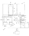
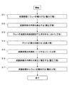
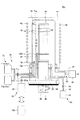
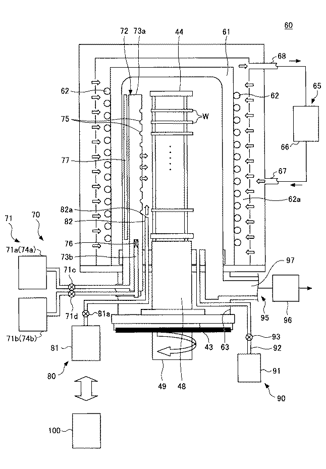
【解決手段】基板にポリイミド膜を成膜する成膜装置において、成膜容器60内に搬入されている基板を加熱する加熱機構62と、成膜容器60内に密着促進剤を気化させた密着促進剤ガスを供給する密着促進剤供給機構80と、加熱機構62と密着促進剤供給機構80とを制御する制御部100とを有する。制御部100は、基板を成膜容器60内に搬入した後、加熱機構62により、基板の温度を、基板にポリイミド膜を成膜するときの所定温度まで上昇させる間に、密着促進剤供給機構80により密着促進剤ガスを成膜容器60内に供給し、基板の表面を密着促進剤ガスにより処理するように、制御する。
【選択図】図4
Description
(第1の実施の形態)
最初に、図1から図15を参照し、本発明の第1の実施の形態に係る成膜装置について説明する。本実施の形態に係る成膜装置は、例えばピロメリット酸二無水物(Pyromellitic Dianhydride、以下「PMDA」と略す。)を気化させた第1の原料ガスと、例えば4,4'−3オキシジアニリン(4,4'-Oxydianiline、以下「ODA」と略す。)を気化させた第2の原料ガスとを、成膜容器内に搬入されている基板に供給することによって、基板にポリイミド膜を成膜する成膜装置に適用することができる。
(第1の実施の形態の変形例)
次に、図16を参照し、本発明の第1の実施の形態の変形例に係る成膜装置について説明する。
(第2の実施の形態)
次に、図17を参照し、本発明の第2の実施の形態に係る成膜装置について説明する。
43 蓋体(基板保持部)
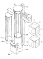
44、44a、44b ボート(基板保持部)
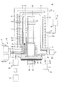
60 成膜容器
65 冷却機構
70 供給機構
71 原料ガス供給部
80 密着促進剤供給機構
90 パージガス供給機構
95 排気機構
100 制御部
W ウェハ
Claims (7)
- 酸二無水物よりなる第1の原料を気化させた第1の原料ガスと、ジアミンよりなる第2の原料を気化させた第2の原料ガスとを、成膜容器内に搬入されている基板に供給することによって、前記基板にポリイミド膜を成膜する成膜装置において、
前記成膜容器内に搬入されている基板を加熱する加熱機構と、
前記成膜容器内に密着促進剤を気化させた密着促進剤ガスを供給する密着促進剤供給機構と、
前記加熱機構と前記密着促進剤供給機構とを制御する制御部と
を有し、
前記制御部は、基板を前記成膜容器内に搬入した後、前記加熱機構により、前記基板の温度を、前記基板にポリイミド膜を成膜するときの所定温度まで上昇させる間に、前記密着促進剤供給機構により前記密着促進剤ガスを前記成膜容器内に供給し、前記基板の表面を前記密着促進剤ガスにより処理するように、制御するものである、成膜装置。 - 前記密着促進剤供給機構は、前記成膜容器内に設けられるとともに、前記密着促進剤ガスを供給するための供給孔が形成された、供給管を含み、前記供給孔を介して前記成膜容器内に前記密着促進剤ガスを供給するものである、請求項1に記載の成膜装置。
- 前記成膜容器内で基板を保持する基板保持部を有し、
前記供給孔は、前記基板保持部に保持されている基板の近傍に配置されている、請求項2に記載の成膜装置。 - 前記成膜容器内に前記第1の原料ガスを供給する第1の原料ガス供給部を有し、
前記制御部は、前記基板の表面を前記密着促進剤ガスにより処理した後、前記基板にポリイミド膜を成膜する前に、前記第1の原料ガス供給部により前記第1の原料ガスを供給し、前記基板の表面を前記第1の原料ガスにより処理するように、制御するものである、請求項1から請求項3のいずれかに記載の成膜装置。 - 前記成膜容器に空気を送風することによって前記成膜容器を冷却する冷却機構を有し、
前記制御部は、前記基板の温度を前記所定温度まで上昇させる際に、前記加熱機構の加熱量と前記冷却機構の冷却量とを制御するものである、請求項1から請求項4のいずれかに記載の成膜装置。 - 前記制御部は、前記基板にポリイミド膜を成膜した後、前記成膜容器内で、前記基板に成膜されたポリイミド膜を前記加熱機構により熱処理するように、制御するものである、請求項1から請求項5のいずれかに記載の成膜装置。
- 前記成膜容器内からガスを排気する排気機構と、
前記成膜容器内にパージガスを供給するパージガス供給機構と
を有し、
前記制御部は、前記基板にポリイミド膜を成膜した後、前記排気機構と前記パージガス供給機構とにより前記成膜容器内のガスをパージガスに置換する際に、前記基板に成膜されたポリイミド膜を前記加熱機構により熱処理するように、制御するものである、請求項6に記載の成膜装置。
Priority Applications (4)
| Application Number | Priority Date | Filing Date | Title |
|---|---|---|---|
| JP2011066461A JP5296132B2 (ja) | 2011-03-24 | 2011-03-24 | 成膜装置 |
| TW101108336A TWI550128B (zh) | 2011-03-24 | 2012-03-12 | 膜沉積裝置 |
| US13/425,483 US20130068163A1 (en) | 2011-03-24 | 2012-03-21 | Film deposition apparatus |
| KR1020120029162A KR101571019B1 (ko) | 2011-03-24 | 2012-03-22 | 성막 장치 |
Applications Claiming Priority (1)
| Application Number | Priority Date | Filing Date | Title |
|---|---|---|---|
| JP2011066461A JP5296132B2 (ja) | 2011-03-24 | 2011-03-24 | 成膜装置 |
Publications (2)
| Publication Number | Publication Date |
|---|---|
| JP2012204518A true JP2012204518A (ja) | 2012-10-22 |
| JP5296132B2 JP5296132B2 (ja) | 2013-09-25 |
Family
ID=47185198
Family Applications (1)
| Application Number | Title | Priority Date | Filing Date |
|---|---|---|---|
| JP2011066461A Active JP5296132B2 (ja) | 2011-03-24 | 2011-03-24 | 成膜装置 |
Country Status (4)
| Country | Link |
|---|---|
| US (1) | US20130068163A1 (ja) |
| JP (1) | JP5296132B2 (ja) |
| KR (1) | KR101571019B1 (ja) |
| TW (1) | TWI550128B (ja) |
Cited By (1)
| Publication number | Priority date | Publication date | Assignee | Title |
|---|---|---|---|---|
| JP2015156460A (ja) * | 2014-02-21 | 2015-08-27 | 東京エレクトロン株式会社 | 重合膜の成膜方法および成膜装置 |
Families Citing this family (6)
| Publication number | Priority date | Publication date | Assignee | Title |
|---|---|---|---|---|
| JP2012080080A (ja) * | 2010-09-07 | 2012-04-19 | Tokyo Electron Ltd | 縦型熱処理装置及びその制御方法 |
| JP5779957B2 (ja) * | 2011-04-20 | 2015-09-16 | 東京エレクトロン株式会社 | ローディングユニット及び処理システム |
| JP6111171B2 (ja) * | 2013-09-02 | 2017-04-05 | 東京エレクトロン株式会社 | 成膜方法及び成膜装置 |
| FR3019159A1 (fr) * | 2014-04-01 | 2015-10-02 | Vincent Ind | Nacelle d'empaquetage de plaquette de silicium, ensemble comprenant une telle nacelle et methode d'empaquetage |
| US10593572B2 (en) * | 2018-03-15 | 2020-03-17 | Kokusai Electric Corporation | Substrate processing apparatus and method of manufacturing semiconductor device |
| CN112575312B (zh) * | 2019-09-30 | 2023-08-29 | 长鑫存储技术有限公司 | 薄膜制备设备以及薄膜制备方法 |
Citations (8)
| Publication number | Priority date | Publication date | Assignee | Title |
|---|---|---|---|---|
| JPS60197730A (ja) * | 1984-03-21 | 1985-10-07 | Ulvac Corp | ポリイミド膜の形成方法 |
| JPH036363A (ja) * | 1989-05-31 | 1991-01-11 | Ulvac Corp | 低比誘電性ポリイミド被膜の形成方法 |
| JPH0313561A (ja) * | 1989-06-09 | 1991-01-22 | Ulvac Corp | ポリイミド樹脂被膜の形成方法 |
| JPH11172418A (ja) * | 1997-12-12 | 1999-06-29 | Ulvac Corp | 成膜装置 |
| JP2000003910A (ja) * | 1998-06-16 | 2000-01-07 | Ulvac Corp | 低比誘電性絶縁膜の形成方法及び層間絶縁膜 |
| JP2006231134A (ja) * | 2005-02-22 | 2006-09-07 | Ulvac Japan Ltd | 有機材料膜の形成方法 |
| JP2009158968A (ja) * | 2006-03-07 | 2009-07-16 | Hitachi Kokusai Electric Inc | 基板処理方法および膜形成方法 |
| WO2009119343A1 (ja) * | 2008-03-25 | 2009-10-01 | 東京エレクトロン株式会社 | 表面処理装置、及び表面処理方法 |
Family Cites Families (11)
| Publication number | Priority date | Publication date | Assignee | Title |
|---|---|---|---|---|
| JPS63289813A (ja) * | 1987-05-21 | 1988-11-28 | Yamaha Corp | 半導体ウエハ熱処理法 |
| JP4283910B2 (ja) * | 1998-07-07 | 2009-06-24 | 株式会社アルバック | 半導体製造装置およびポリイミド膜の形成方法 |
| JP4493192B2 (ja) * | 2000-09-13 | 2010-06-30 | 東京エレクトロン株式会社 | バッチ式熱処理装置及びその制御方法 |
| US6656313B2 (en) * | 2001-06-11 | 2003-12-02 | International Business Machines Corporation | Structure and method for improved adhesion between two polymer films |
| DE10259728B4 (de) * | 2002-12-19 | 2008-01-17 | Advanced Micro Devices, Inc., Sunnyvale | Verfahren zur Herstellung einer Grabenisolationsstruktur und Verfahren zum Steuern eines Grades an Kantenrundung einer Grabenisolationsstruktur in einem Halbleiterbauelement |
| US7727780B2 (en) * | 2007-01-26 | 2010-06-01 | Hitachi Kokusai Electric Inc. | Substrate processing method and semiconductor manufacturing apparatus |
| JP2009119343A (ja) * | 2007-11-13 | 2009-06-04 | Seiko Epson Corp | タンク収納装置 |
| TWI364126B (en) * | 2007-11-23 | 2012-05-11 | Ind Tech Res Inst | Plasma assisted apparatus for forming organic film |
| JP5322468B2 (ja) * | 2008-03-25 | 2013-10-23 | 富士フイルム株式会社 | 放射線検出器の製造方法及び成膜装置 |
| JP2010024484A (ja) | 2008-07-17 | 2010-02-04 | Seiko Epson Corp | 表面処理装置および表面処理方法 |
| JP2010219147A (ja) | 2009-03-13 | 2010-09-30 | Tokyo Electron Ltd | 成膜装置、気化器、制御プログラム及びコンピュータ読取可能な記憶媒体 |
-
2011
- 2011-03-24 JP JP2011066461A patent/JP5296132B2/ja active Active
-
2012
- 2012-03-12 TW TW101108336A patent/TWI550128B/zh active
- 2012-03-21 US US13/425,483 patent/US20130068163A1/en not_active Abandoned
- 2012-03-22 KR KR1020120029162A patent/KR101571019B1/ko active Active
Patent Citations (8)
| Publication number | Priority date | Publication date | Assignee | Title |
|---|---|---|---|---|
| JPS60197730A (ja) * | 1984-03-21 | 1985-10-07 | Ulvac Corp | ポリイミド膜の形成方法 |
| JPH036363A (ja) * | 1989-05-31 | 1991-01-11 | Ulvac Corp | 低比誘電性ポリイミド被膜の形成方法 |
| JPH0313561A (ja) * | 1989-06-09 | 1991-01-22 | Ulvac Corp | ポリイミド樹脂被膜の形成方法 |
| JPH11172418A (ja) * | 1997-12-12 | 1999-06-29 | Ulvac Corp | 成膜装置 |
| JP2000003910A (ja) * | 1998-06-16 | 2000-01-07 | Ulvac Corp | 低比誘電性絶縁膜の形成方法及び層間絶縁膜 |
| JP2006231134A (ja) * | 2005-02-22 | 2006-09-07 | Ulvac Japan Ltd | 有機材料膜の形成方法 |
| JP2009158968A (ja) * | 2006-03-07 | 2009-07-16 | Hitachi Kokusai Electric Inc | 基板処理方法および膜形成方法 |
| WO2009119343A1 (ja) * | 2008-03-25 | 2009-10-01 | 東京エレクトロン株式会社 | 表面処理装置、及び表面処理方法 |
Cited By (2)
| Publication number | Priority date | Publication date | Assignee | Title |
|---|---|---|---|---|
| JP2015156460A (ja) * | 2014-02-21 | 2015-08-27 | 東京エレクトロン株式会社 | 重合膜の成膜方法および成膜装置 |
| US9683128B2 (en) | 2014-02-21 | 2017-06-20 | Tokyo Electron Limited | Polymerized film forming method |
Also Published As
| Publication number | Publication date |
|---|---|
| KR101571019B1 (ko) | 2015-11-23 |
| TWI550128B (zh) | 2016-09-21 |
| JP5296132B2 (ja) | 2013-09-25 |
| US20130068163A1 (en) | 2013-03-21 |
| TW201305384A (zh) | 2013-02-01 |
| KR20120109344A (ko) | 2012-10-08 |
Similar Documents
| Publication | Publication Date | Title |
|---|---|---|
| JP5296132B2 (ja) | 成膜装置 | |
| JP2012209393A (ja) | クリーニング方法及び成膜方法 | |
| TWI532867B (zh) | 成膜裝置(一) | |
| US20140235068A1 (en) | Method of manufacturing semiconductor device, apparatus for manufacturing semiconductor device, and non-transitory computer-readable recording medium | |
| US8691338B2 (en) | Polymerized film forming method and polymerized film forming apparatus | |
| CN102468158A (zh) | 衬底处理设备和制造半导体器件的方法 | |
| JP5350424B2 (ja) | 表面処理方法 | |
| JP5195640B2 (ja) | 熱処理装置 | |
| CN113597666B (zh) | 半导体装置的制造方法、基板处理装置和存储介质 | |
| CN115917712A (zh) | 基板处理装置、半导体装置的制造方法以及等离子体生成装置 | |
| JP6276428B2 (ja) | 基板処理装置、半導体装置の製造方法、及びサセプタ | |
| JP2012204519A (ja) | 表面処理方法及び成膜方法 | |
| US9683128B2 (en) | Polymerized film forming method | |
| JP2010171347A (ja) | 成膜方法 | |
| JPH1092754A (ja) | 枚葉式の熱処理装置及び熱処理方法 | |
| US20150232702A1 (en) | Polymerized film forming method and polymerized film forming apparatus | |
| JP2005236283A (ja) | ウェーハ上に膜を形成する方法 | |
| WO2016052333A1 (ja) | 基板処理装置、半導体装置の製造方法及び記録媒体 | |
| JPS6381933A (ja) | 枚葉式薄膜形成方法 | |
| CN118086867A (zh) | 成膜方法和成膜装置 | |
| JP2013089833A (ja) | 半導体装置の製造方法 | |
| JP2014187258A (ja) | 基板処理装置及び半導体装置の製造方法 |
Legal Events
| Date | Code | Title | Description |
|---|---|---|---|
| A977 | Report on retrieval |
Free format text: JAPANESE INTERMEDIATE CODE: A971007 Effective date: 20130314 |
|
| A131 | Notification of reasons for refusal |
Free format text: JAPANESE INTERMEDIATE CODE: A131 Effective date: 20130326 |
|
| A521 | Request for written amendment filed |
Free format text: JAPANESE INTERMEDIATE CODE: A523 Effective date: 20130515 |
|
| TRDD | Decision of grant or rejection written | ||
| A01 | Written decision to grant a patent or to grant a registration (utility model) |
Free format text: JAPANESE INTERMEDIATE CODE: A01 Effective date: 20130604 |
|
| A61 | First payment of annual fees (during grant procedure) |
Free format text: JAPANESE INTERMEDIATE CODE: A61 Effective date: 20130612 |
|
| R150 | Certificate of patent or registration of utility model |
Ref document number: 5296132 Country of ref document: JP Free format text: JAPANESE INTERMEDIATE CODE: R150 Free format text: JAPANESE INTERMEDIATE CODE: R150 |
|
| R250 | Receipt of annual fees |
Free format text: JAPANESE INTERMEDIATE CODE: R250 |
|
| R250 | Receipt of annual fees |
Free format text: JAPANESE INTERMEDIATE CODE: R250 |
|
| R250 | Receipt of annual fees |
Free format text: JAPANESE INTERMEDIATE CODE: R250 |
|
| R250 | Receipt of annual fees |
Free format text: JAPANESE INTERMEDIATE CODE: R250 |
|
| R250 | Receipt of annual fees |
Free format text: JAPANESE INTERMEDIATE CODE: R250 |
|
| R250 | Receipt of annual fees |
Free format text: JAPANESE INTERMEDIATE CODE: R250 |
|
| R250 | Receipt of annual fees |
Free format text: JAPANESE INTERMEDIATE CODE: R250 |
|
| R250 | Receipt of annual fees |
Free format text: JAPANESE INTERMEDIATE CODE: R250 |