JP2012244122A - 半導体レーザ素子破壊防止回路、及びそれを備える光ディスク装置 - Google Patents
半導体レーザ素子破壊防止回路、及びそれを備える光ディスク装置 Download PDFInfo
- Publication number
- JP2012244122A JP2012244122A JP2011116148A JP2011116148A JP2012244122A JP 2012244122 A JP2012244122 A JP 2012244122A JP 2011116148 A JP2011116148 A JP 2011116148A JP 2011116148 A JP2011116148 A JP 2011116148A JP 2012244122 A JP2012244122 A JP 2012244122A
- Authority
- JP
- Japan
- Prior art keywords
- light emission
- semiconductor laser
- voltage
- laser element
- circuit unit
- Prior art date
- Legal status (The legal status is an assumption and is not a legal conclusion. Google has not performed a legal analysis and makes no representation as to the accuracy of the status listed.)
- Pending
Links
- 230000003287 optical effect Effects 0.000 title claims abstract description 84
- 239000004065 semiconductor Substances 0.000 title claims abstract description 73
- 230000002265 prevention Effects 0.000 title claims abstract description 28
- 230000015556 catabolic process Effects 0.000 title abstract description 11
- 238000012544 monitoring process Methods 0.000 claims abstract description 42
- 230000005856 abnormality Effects 0.000 claims abstract description 10
- 230000006378 damage Effects 0.000 claims description 20
- 238000006243 chemical reaction Methods 0.000 description 12
- 238000012545 processing Methods 0.000 description 8
- 238000010586 diagram Methods 0.000 description 6
- 230000002159 abnormal effect Effects 0.000 description 5
- 230000004044 response Effects 0.000 description 5
- 230000005236 sound signal Effects 0.000 description 4
- 238000004519 manufacturing process Methods 0.000 description 3
- 230000004048 modification Effects 0.000 description 2
- 238000012986 modification Methods 0.000 description 2
- 238000013459 approach Methods 0.000 description 1
- 239000003990 capacitor Substances 0.000 description 1
- 230000008859 change Effects 0.000 description 1
- 239000000470 constituent Substances 0.000 description 1
- 230000000994 depressogenic effect Effects 0.000 description 1
- 238000001514 detection method Methods 0.000 description 1
- 230000004069 differentiation Effects 0.000 description 1
- 239000000284 extract Substances 0.000 description 1
- 238000000034 method Methods 0.000 description 1
- 230000008569 process Effects 0.000 description 1
Images
Classifications
-
- H—ELECTRICITY
- H01—ELECTRIC ELEMENTS
- H01S—DEVICES USING THE PROCESS OF LIGHT AMPLIFICATION BY STIMULATED EMISSION OF RADIATION [LASER] TO AMPLIFY OR GENERATE LIGHT; DEVICES USING STIMULATED EMISSION OF ELECTROMAGNETIC RADIATION IN WAVE RANGES OTHER THAN OPTICAL
- H01S5/00—Semiconductor lasers
- H01S5/04—Processes or apparatus for excitation, e.g. pumping, e.g. by electron beams
- H01S5/042—Electrical excitation ; Circuits therefor
-
- G—PHYSICS
- G11—INFORMATION STORAGE
- G11B—INFORMATION STORAGE BASED ON RELATIVE MOVEMENT BETWEEN RECORD CARRIER AND TRANSDUCER
- G11B7/00—Recording or reproducing by optical means, e.g. recording using a thermal beam of optical radiation by modifying optical properties or the physical structure, reproducing using an optical beam at lower power by sensing optical properties; Record carriers therefor
- G11B7/12—Heads, e.g. forming of the optical beam spot or modulation of the optical beam
- G11B7/125—Optical beam sources therefor, e.g. laser control circuitry specially adapted for optical storage devices; Modulators, e.g. means for controlling the size or intensity of optical spots or optical traces
- G11B7/126—Circuits, methods or arrangements for laser control or stabilisation
- G11B7/1263—Power control during transducing, e.g. by monitoring
-
- H—ELECTRICITY
- H01—ELECTRIC ELEMENTS
- H01S—DEVICES USING THE PROCESS OF LIGHT AMPLIFICATION BY STIMULATED EMISSION OF RADIATION [LASER] TO AMPLIFY OR GENERATE LIGHT; DEVICES USING STIMULATED EMISSION OF ELECTROMAGNETIC RADIATION IN WAVE RANGES OTHER THAN OPTICAL
- H01S5/00—Semiconductor lasers
- H01S5/06—Arrangements for controlling the laser output parameters, e.g. by operating on the active medium
- H01S5/068—Stabilisation of laser output parameters
- H01S5/06825—Protecting the laser, e.g. during switch-on/off, detection of malfunctioning or degradation
Landscapes
- Physics & Mathematics (AREA)
- Optics & Photonics (AREA)
- Condensed Matter Physics & Semiconductors (AREA)
- General Physics & Mathematics (AREA)
- Electromagnetism (AREA)
- Optical Head (AREA)
- Semiconductor Lasers (AREA)
Abstract
【解決手段】
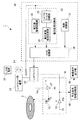
光ディスク装置の半導体レーザ素子破壊防止回路が、半導体レーザ素子の発光を指示する旨の発光指示信号を出力する発光指示回路部と、半導体レーザ素子を発光させるために半導体レーザ素子用電源から光出力制御回路部に供給される発光電圧を監視し、発光電圧に異常がないと判断するとき、半導体レーザ素子の発光を許可する旨の発光許可信号を出力する電圧監視回路部と、発光指示信号及び発光許可信号が入力されるときのみ、光出力制御回路部に半導体レーザ素子を発光させる発光許可回路部と、を備える。
【選択図】図1
Description
2 光学ディスク
10 光ピックアップ部
11 レーザダイオード、LD(半導体レーザ素子)
12 ビームスプリッタ
13 フォトダイオード、PD
21 LDドライバ(光出力制御回路部)
22 LD用電源(半導体レーザ素子用電源)
23 LDドライバ用電源
24 スイッチ回路部
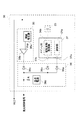
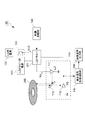
30 LD破壊防止回路(半導体レーザ素子破壊防止回路)
31 制御回路部(発光指示回路部)
31a 制御部(発光指示部)
32 電圧監視回路部
33 ハイパスフィルタ回路部(フィルタ回路部)
34 電圧変動監視回路部
34a 電圧変動監視部
35 電圧値監視回路部
35a 閾値電圧源
35b コンパレータ(比較回路部)
36 AND回路部(発光許可回路部)
36a 第1ダイオード(第1整流素子)
36b 第2ダイオード(第2整流素子の1つ)
36c 第3ダイオード(第2整流素子の1つ)
36d 基準電源
37 メインLSI
37a 第1出力端子部
37b 第2出力端子部
40 再生信号処理回路部
50 映像音声出力部
Claims (6)
- 半導体レーザ素子の発光を指示する旨の発光指示信号を出力する発光指示回路部と、
前記半導体レーザ素子を発光させるために半導体レーザ素子用電源から光出力制御回路部に供給される発光電圧を監視し、発光電圧に異常がないと判断するとき、前記半導体レーザ素子の発光を許可する旨の発光許可信号を出力する電圧監視回路部と、
前記発光指示信号及び前記発光許可信号が入力されるときのみ、前記光出力制御回路部に前記半導体レーザ素子を発光させる発光許可回路部と、
を備えることを特徴とする半導体レーザ素子破壊防止回路。 - 前記電圧監視回路部は、前記発光電圧の電圧値、及び前記電圧値の変動成分の大きさのうちの少なくとも一方に異常がないと判断するとき、前記発光許可信号を出力することを特徴とする請求項1に記載の半導体レーザ素子破壊防止回路。
- 前記発光許可回路部が、
前記発光指示回路部の出力側にカソードが接続される第1整流素子と、
前記電圧監視回路部の出力側にカソードが接続される少なくとも1つの第2整流素子と、
第1及び第2整流素子のアノードにプルアップ抵抗素子を介して基準電位を与える基準電源と、
を有し、
第1及び第2整流素子のアノードが前記光出力制御回路部に接続され、
前記発光指示回路部は、前記半導体レーザ素子の発光停止を指示するとき、第1整流素子を導通させ、
前記電圧監視回路部は、前記発光電圧の電圧値及び前記変動成分の大きさのうちの少なくとも一方に異常があると判断するとき、第2整流素子を導通させることを特徴とする請求項1又は請求項2に記載の半導体レーザ素子破壊防止回路。 - 前記発光指示回路部と、前記電圧監視回路部の少なくとも一部とが、1つのマイクロコンピュータに設けられることを特徴とする請求項1〜請求項3のいずれかに記載の半導体レーザ素子破壊防止回路。
- 前記電圧監視回路部は、前記発光電圧の電圧値が前記半導体レーザ素子を発光させるために必要な最小の動作電圧値以上であるとき、前記発光電圧の電圧値に異常がないと判断することを特徴とする請求項1〜請求項4のいずれかに記載の半導体レーザ素子破壊防止回路。
- 半導体レーザ素子を有する光ピックアップ部と、
前記半導体レーザ素子の光出力制御を行う光出力制御回路部と、
前記半導体レーザ素子を発光させるための発光電圧を前記光出力制御回路部に供給する半導体レーザ素子用電源と、
請求項1〜請求項5のいずれかに記載の半導体レーザ素子破壊防止回路と、
を備えることを特徴とする光ディスク装置。
Priority Applications (2)
| Application Number | Priority Date | Filing Date | Title |
|---|---|---|---|
| JP2011116148A JP2012244122A (ja) | 2011-05-24 | 2011-05-24 | 半導体レーザ素子破壊防止回路、及びそれを備える光ディスク装置 |
| US13/449,740 US8411549B2 (en) | 2011-05-24 | 2012-04-18 | Circuit for preventing destruction of semiconductor laser element, and optical disc device provided with the circuit |
Applications Claiming Priority (1)
| Application Number | Priority Date | Filing Date | Title |
|---|---|---|---|
| JP2011116148A JP2012244122A (ja) | 2011-05-24 | 2011-05-24 | 半導体レーザ素子破壊防止回路、及びそれを備える光ディスク装置 |
Publications (1)
| Publication Number | Publication Date |
|---|---|
| JP2012244122A true JP2012244122A (ja) | 2012-12-10 |
Family
ID=47219158
Family Applications (1)
| Application Number | Title | Priority Date | Filing Date |
|---|---|---|---|
| JP2011116148A Pending JP2012244122A (ja) | 2011-05-24 | 2011-05-24 | 半導体レーザ素子破壊防止回路、及びそれを備える光ディスク装置 |
Country Status (2)
| Country | Link |
|---|---|
| US (1) | US8411549B2 (ja) |
| JP (1) | JP2012244122A (ja) |
Citations (4)
| Publication number | Priority date | Publication date | Assignee | Title |
|---|---|---|---|---|
| JPH04241485A (ja) * | 1991-01-16 | 1992-08-28 | Ricoh Co Ltd | レーザダイオード保護装置 |
| JPH04255284A (ja) * | 1991-02-07 | 1992-09-10 | Pioneer Electron Corp | レーザダイオードの駆動制御装置 |
| JPH04291776A (ja) * | 1991-03-20 | 1992-10-15 | Hitachi Ltd | 半導体レーザ駆動回路 |
| JP2004229275A (ja) * | 2003-01-21 | 2004-08-12 | Hewlett-Packard Development Co Lp | 論理ゲート |
Family Cites Families (4)
| Publication number | Priority date | Publication date | Assignee | Title |
|---|---|---|---|---|
| US5666045A (en) * | 1994-12-09 | 1997-09-09 | Psc Inc. | Laser drive and control systems useful for laser diode protection |
| US6108114A (en) * | 1998-01-22 | 2000-08-22 | Methode Electronics, Inc. | Optoelectronic transmitter having an improved power control circuit for rapidly enabling a semiconductor laser |
| JP2004355697A (ja) | 2003-05-28 | 2004-12-16 | Sankyo Seiki Mfg Co Ltd | 光ピックアップのレーザダイオード出力調整回路 |
| JP4155189B2 (ja) * | 2003-12-25 | 2008-09-24 | 株式会社日立製作所 | 光ディスク装置及びデータ再生方法 |
-
2011
- 2011-05-24 JP JP2011116148A patent/JP2012244122A/ja active Pending
-
2012
- 2012-04-18 US US13/449,740 patent/US8411549B2/en not_active Expired - Fee Related
Patent Citations (4)
| Publication number | Priority date | Publication date | Assignee | Title |
|---|---|---|---|---|
| JPH04241485A (ja) * | 1991-01-16 | 1992-08-28 | Ricoh Co Ltd | レーザダイオード保護装置 |
| JPH04255284A (ja) * | 1991-02-07 | 1992-09-10 | Pioneer Electron Corp | レーザダイオードの駆動制御装置 |
| JPH04291776A (ja) * | 1991-03-20 | 1992-10-15 | Hitachi Ltd | 半導体レーザ駆動回路 |
| JP2004229275A (ja) * | 2003-01-21 | 2004-08-12 | Hewlett-Packard Development Co Lp | 論理ゲート |
Also Published As
| Publication number | Publication date |
|---|---|
| US8411549B2 (en) | 2013-04-02 |
| US20120300605A1 (en) | 2012-11-29 |
Similar Documents
| Publication | Publication Date | Title |
|---|---|---|
| JP2011015193A (ja) | 音声出力装置 | |
| US7924689B2 (en) | Optical disk apparatus | |
| JP4220349B2 (ja) | 光ピックアップシステムのモニタフォトダイオード利得制御装置 | |
| US8009546B2 (en) | Over current protection device | |
| US8411549B2 (en) | Circuit for preventing destruction of semiconductor laser element, and optical disc device provided with the circuit | |
| KR101138467B1 (ko) | 전류 구동 회로 및 이를 포함한 광 스토리지 시스템 | |
| JP2005531865A (ja) | さまざまな光記録媒体の再生又は記録装置のための本質的に安全なピックアップ | |
| JPH0816988B2 (ja) | 光学式デ−タ記憶再生装置 | |
| US7869311B2 (en) | Built-in type optical disc apparatus | |
| US20110199673A1 (en) | Integrated optical device and optical pickup device using the same | |
| JP2010287275A (ja) | 光ディスク再生装置 | |
| KR100656160B1 (ko) | 광픽업장치 | |
| KR100621376B1 (ko) | 모니터링용 광검출장치 및 이를 적용한 광픽업장치 | |
| US8134897B2 (en) | Current gain control system | |
| JPH04255284A (ja) | レーザダイオードの駆動制御装置 | |
| JP2011108296A (ja) | 光ピックアップ及びそれを備えた光ディスク装置 | |
| KR100646794B1 (ko) | 광디스크 플레이어용 광픽업장치의 레이저 다이오드 수명감시장치 | |
| JP2008016107A (ja) | 光ピックアップ装置および光ディスクドライブ | |
| JPH0992922A (ja) | 半導体レーザ駆動回路 | |
| KR20060122305A (ko) | 광 기록/재생기기의 인터페이스장치 | |
| JP2006237177A (ja) | 半導体レーザ制御装置 | |
| JP2004355697A (ja) | 光ピックアップのレーザダイオード出力調整回路 | |
| JP2011108297A (ja) | 光ピックアップ及びそれを備えた光ディスク装置 | |
| JP2012256396A (ja) | 光ディスク装置、及び光ディスク装置の再生パワー設定方法 | |
| JPH10312569A (ja) | 光学的記録再生装置 |
Legal Events
| Date | Code | Title | Description |
|---|---|---|---|
| A977 | Report on retrieval |
Free format text: JAPANESE INTERMEDIATE CODE: A971007 Effective date: 20130318 |
|
| A131 | Notification of reasons for refusal |
Free format text: JAPANESE INTERMEDIATE CODE: A131 Effective date: 20130326 |
|
| A521 | Request for written amendment filed |
Free format text: JAPANESE INTERMEDIATE CODE: A523 Effective date: 20130527 |
|
| A131 | Notification of reasons for refusal |
Free format text: JAPANESE INTERMEDIATE CODE: A131 Effective date: 20130917 |
|
| A02 | Decision of refusal |
Free format text: JAPANESE INTERMEDIATE CODE: A02 Effective date: 20140204 |