JP2012506132A - 埋め込みプロセスの温度調整方法 - Google Patents
埋め込みプロセスの温度調整方法 Download PDFInfo
- Publication number
- JP2012506132A JP2012506132A JP2011530165A JP2011530165A JP2012506132A JP 2012506132 A JP2012506132 A JP 2012506132A JP 2011530165 A JP2011530165 A JP 2011530165A JP 2011530165 A JP2011530165 A JP 2011530165A JP 2012506132 A JP2012506132 A JP 2012506132A
- Authority
- JP
- Japan
- Prior art keywords
- temperature
- substrate
- ions
- embedding
- ion implantation
- Prior art date
- Legal status (The legal status is an assumption and is not a legal conclusion. Google has not performed a legal analysis and makes no representation as to the accuracy of the status listed.)
- Granted
Links
Images


Classifications
-
- H—ELECTRICITY
- H10—SEMICONDUCTOR DEVICES; ELECTRIC SOLID-STATE DEVICES NOT OTHERWISE PROVIDED FOR
- H10P—GENERIC PROCESSES OR APPARATUS FOR THE MANUFACTURE OR TREATMENT OF DEVICES COVERED BY CLASS H10
- H10P30/00—Ion implantation into wafers, substrates or parts of devices
- H10P30/20—Ion implantation into wafers, substrates or parts of devices into semiconductor materials, e.g. for doping
- H10P30/21—Ion implantation into wafers, substrates or parts of devices into semiconductor materials, e.g. for doping of electrically active species
-
- H—ELECTRICITY
- H10—SEMICONDUCTOR DEVICES; ELECTRIC SOLID-STATE DEVICES NOT OTHERWISE PROVIDED FOR
- H10P—GENERIC PROCESSES OR APPARATUS FOR THE MANUFACTURE OR TREATMENT OF DEVICES COVERED BY CLASS H10
- H10P30/00—Ion implantation into wafers, substrates or parts of devices
- H10P30/20—Ion implantation into wafers, substrates or parts of devices into semiconductor materials, e.g. for doping
- H10P30/202—Ion implantation into wafers, substrates or parts of devices into semiconductor materials, e.g. for doping characterised by the semiconductor materials
- H10P30/204—Ion implantation into wafers, substrates or parts of devices into semiconductor materials, e.g. for doping characterised by the semiconductor materials into Group IV semiconductors
-
- H—ELECTRICITY
- H10—SEMICONDUCTOR DEVICES; ELECTRIC SOLID-STATE DEVICES NOT OTHERWISE PROVIDED FOR
- H10P—GENERIC PROCESSES OR APPARATUS FOR THE MANUFACTURE OR TREATMENT OF DEVICES COVERED BY CLASS H10
- H10P30/00—Ion implantation into wafers, substrates or parts of devices
- H10P30/20—Ion implantation into wafers, substrates or parts of devices into semiconductor materials, e.g. for doping
- H10P30/225—Ion implantation into wafers, substrates or parts of devices into semiconductor materials, e.g. for doping of a molecular ion, e.g. decaborane
-
- H—ELECTRICITY
- H10—SEMICONDUCTOR DEVICES; ELECTRIC SOLID-STATE DEVICES NOT OTHERWISE PROVIDED FOR
- H10P—GENERIC PROCESSES OR APPARATUS FOR THE MANUFACTURE OR TREATMENT OF DEVICES COVERED BY CLASS H10
- H10P30/00—Ion implantation into wafers, substrates or parts of devices
- H10P30/20—Ion implantation into wafers, substrates or parts of devices into semiconductor materials, e.g. for doping
- H10P30/226—Ion implantation into wafers, substrates or parts of devices into semiconductor materials, e.g. for doping at a temperature lower than room temperature
-
- H—ELECTRICITY
- H10—SEMICONDUCTOR DEVICES; ELECTRIC SOLID-STATE DEVICES NOT OTHERWISE PROVIDED FOR
- H10P—GENERIC PROCESSES OR APPARATUS FOR THE MANUFACTURE OR TREATMENT OF DEVICES COVERED BY CLASS H10
- H10P30/00—Ion implantation into wafers, substrates or parts of devices
- H10P30/40—Ion implantation into wafers, substrates or parts of devices into insulating materials
-
- H—ELECTRICITY
- H10—SEMICONDUCTOR DEVICES; ELECTRIC SOLID-STATE DEVICES NOT OTHERWISE PROVIDED FOR
- H10P—GENERIC PROCESSES OR APPARATUS FOR THE MANUFACTURE OR TREATMENT OF DEVICES COVERED BY CLASS H10
- H10P32/00—Diffusion of dopants within, into or out of wafers, substrates or parts of devices
- H10P32/10—Diffusion of dopants within, into or out of semiconductor bodies or layers
- H10P32/14—Diffusion of dopants within, into or out of semiconductor bodies or layers within a single semiconductor body or layer in a solid phase; between different semiconductor bodies or layers, both in a solid phase
- H10P32/1404—Diffusion of dopants within, into or out of semiconductor bodies or layers within a single semiconductor body or layer in a solid phase; between different semiconductor bodies or layers, both in a solid phase using predeposition followed by drive-in of impurities into the semiconductor surface, e.g. predeposition from a gaseous phase
- H10P32/1406—Diffusion of dopants within, into or out of semiconductor bodies or layers within a single semiconductor body or layer in a solid phase; between different semiconductor bodies or layers, both in a solid phase using predeposition followed by drive-in of impurities into the semiconductor surface, e.g. predeposition from a gaseous phase by ion implantation
-
- H—ELECTRICITY
- H10—SEMICONDUCTOR DEVICES; ELECTRIC SOLID-STATE DEVICES NOT OTHERWISE PROVIDED FOR
- H10P—GENERIC PROCESSES OR APPARATUS FOR THE MANUFACTURE OR TREATMENT OF DEVICES COVERED BY CLASS H10
- H10P32/00—Diffusion of dopants within, into or out of wafers, substrates or parts of devices
- H10P32/10—Diffusion of dopants within, into or out of semiconductor bodies or layers
- H10P32/17—Diffusion of dopants within, into or out of semiconductor bodies or layers characterised by the semiconductor material
- H10P32/171—Diffusion of dopants within, into or out of semiconductor bodies or layers characterised by the semiconductor material being group IV material
-
- H—ELECTRICITY
- H10—SEMICONDUCTOR DEVICES; ELECTRIC SOLID-STATE DEVICES NOT OTHERWISE PROVIDED FOR
- H10P—GENERIC PROCESSES OR APPARATUS FOR THE MANUFACTURE OR TREATMENT OF DEVICES COVERED BY CLASS H10
- H10P32/00—Diffusion of dopants within, into or out of wafers, substrates or parts of devices
- H10P32/30—Diffusion for doping of conductive or resistive layers
- H10P32/302—Doping polycrystalline silicon or amorphous silicon layers
-
- H—ELECTRICITY
- H10—SEMICONDUCTOR DEVICES; ELECTRIC SOLID-STATE DEVICES NOT OTHERWISE PROVIDED FOR
- H10P—GENERIC PROCESSES OR APPARATUS FOR THE MANUFACTURE OR TREATMENT OF DEVICES COVERED BY CLASS H10
- H10P95/00—Generic processes or apparatus for manufacture or treatments not covered by the other groups of this subclass
- H10P95/90—Thermal treatments, e.g. annealing or sintering
Landscapes
- Insulated Gate Type Field-Effect Transistor (AREA)
- Physical Vapour Deposition (AREA)
Abstract
Description
Claims (21)
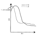
- イオン埋め込みプロセスの間に基板中の不要な二次ドーパントを最小限にする方法であって:
a.前記プロセスの第1の部分の間に第1の温度で前記基板に分子イオンを埋め込み、前記分子イオンを、前記基板との衝突により、所望の一次ドーパントおよび不要な二次ドーパントに分ける工程;および
b.前記埋め込みプロセスの第2の部分の間に前記基板の温度を上昇させ、前記不要な二次ドーパントを前記基板の表面から拡散させる工程;
を備えることを特徴とする方法。 - 前記第1の温度が室温未満である、請求項1に記載の方法。
- 前記第1の温度が−100℃と−10℃との間である、請求項2に記載の方法。
- 前記温度が室温を超えて上昇する、請求項1に記載の方法。
- 前記温度が100℃を超えた温度まで上昇する、請求項4に記載の方法。
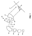
- 埋め込みプロセスの間にイオンを基板に埋め込むための方法であって:
a.第1の温度で前記イオンの部分を前記基板に埋め込む工程;および
b.第2の温度で前記イオンの第2の部分を前記基板に埋め込む工程;
を備えることを特徴とする方法。 - 前記基板が、エピタキシャル成長したソースおよびドレイン領域、多結晶シリコン、高い誘電率を有する材料(HiK材料)、金属および誘電体からなるグループから選択され、前記第1の温度が前記第2の温度よりも高い、請求項6に記載の方法。
- 前記第1の温度が100℃より高い、請求項7に記載の方法。
- 前記第2の温度が−100℃と−10℃との間である、請求項7に記載の方法。
- 前記イオンが、所望および不要の二次ドーパントを有する分子イオンを備え、前記第1の温度が前記第2の温度よりも低い、請求項6に記載の方法。
- 前記第1の温度が−100℃と−10℃との間である、請求項10に記載の方法。
- 前記第2の温度が100℃より高い、請求項10に記載の方法。
- さらに、第3の温度で前記イオンの第3の部分を埋め込む工程を備える、請求項6に記載の方法。
- 前記第1および第3の温度が同じである、請求項13に記載の方法。
- 前記第2の温度が前記3つの温度のうちの最大の温度である、請求項13に記載の方法。
- 前記第2の温度が前記3つの温度のうちの最小の温度である、請求項13に記載の方法。
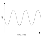
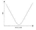
- 埋め込みプロセスの間にイオンを基板に埋め込むための方法であって;
a.一定でない温度プロファイルを作製する工程;
b.第1の温度で前記イオンの部分を前記基板に埋め込む工程;および
c.第2の温度で前記イオンの第2の部分を前記基板に埋め込む工程;
を備えること特徴とする方法。 - 前記プロフィルが不連続の温度ステップを備える、請求項17に記載の方法。
- 前記プロファイルが直線状の傾斜を備える、請求項17に記載の方法。
- 前記プロファイルが指数関数状の傾斜を備える、請求項17に記載の方法。
- 前記プロファイルが正弦曲線である、請求項17に記載の方法。
Applications Claiming Priority (3)
| Application Number | Priority Date | Filing Date | Title |
|---|---|---|---|
| US12/243,992 US7868306B2 (en) | 2008-10-02 | 2008-10-02 | Thermal modulation of implant process |
| US12/243,992 | 2008-10-02 | ||
| PCT/US2009/058988 WO2010039807A2 (en) | 2008-10-02 | 2009-09-30 | Thermal modulation of implant process |
Publications (3)
| Publication Number | Publication Date |
|---|---|
| JP2012506132A true JP2012506132A (ja) | 2012-03-08 |
| JP2012506132A5 JP2012506132A5 (ja) | 2012-10-25 |
| JP5543473B2 JP5543473B2 (ja) | 2014-07-09 |
Family
ID=42074178
Family Applications (1)
| Application Number | Title | Priority Date | Filing Date |
|---|---|---|---|
| JP2011530165A Active JP5543473B2 (ja) | 2008-10-02 | 2009-09-30 | 埋め込みプロセスの温度調整方法 |
Country Status (6)
| Country | Link |
|---|---|
| US (1) | US7868306B2 (ja) |
| JP (1) | JP5543473B2 (ja) |
| KR (1) | KR20110074569A (ja) |
| CN (1) | CN102203913B (ja) |
| TW (1) | TWI451482B (ja) |
| WO (1) | WO2010039807A2 (ja) |
Cited By (1)
| Publication number | Priority date | Publication date | Assignee | Title |
|---|---|---|---|---|
| JP2017112276A (ja) * | 2015-12-17 | 2017-06-22 | 株式会社Sumco | 半導体エピタキシャルウェーハの製造方法および固体撮像素子の製造方法 |
Families Citing this family (11)
| Publication number | Priority date | Publication date | Assignee | Title |
|---|---|---|---|---|
| US8598006B2 (en) * | 2010-03-16 | 2013-12-03 | International Business Machines Corporation | Strain preserving ion implantation methods |
| US8039374B2 (en) * | 2010-03-19 | 2011-10-18 | Advanced Ion Beam Technology, Inc. | Method for low temperature ion implantation |
| US8124508B2 (en) * | 2010-03-31 | 2012-02-28 | Advanced Ion Beam Technology, Inc. | Method for low temperature ion implantation |
| US8586460B2 (en) * | 2010-09-23 | 2013-11-19 | Varian Semiconductor Equipment Associates, Inc. | Controlling laser annealed junction depth by implant modification |
| KR101215649B1 (ko) * | 2011-02-14 | 2012-12-26 | 에스케이하이닉스 주식회사 | 반도체 소자의 형성방법 |
| US8536072B2 (en) * | 2012-02-07 | 2013-09-17 | United Microelectronics Corp. | Semiconductor process |
| US8999800B2 (en) * | 2012-12-12 | 2015-04-07 | Varian Semiconductor Equipment Associates, Inc. | Method of reducing contact resistance |
| KR102274771B1 (ko) * | 2014-03-10 | 2021-07-09 | 에스케이하이닉스 주식회사 | 트랜지스터, 트랜지스터의 제조 방법 및 트랜지스터를 포함하는 전자장치 |
| KR20160061615A (ko) * | 2014-11-24 | 2016-06-01 | 삼성전자주식회사 | 반도체 장치의 제조 방법 |
| WO2016148855A1 (en) | 2015-03-19 | 2016-09-22 | Applied Materials, Inc. | Method and apparatus for reducing radiation induced change in semiconductor structures |
| CN113948375A (zh) * | 2020-07-16 | 2022-01-18 | 珠海格力电器股份有限公司 | 一种提高半导体有源区杂质激活率的方法及其应用 |
Citations (11)
| Publication number | Priority date | Publication date | Assignee | Title |
|---|---|---|---|---|
| JPS62235726A (ja) * | 1986-04-07 | 1987-10-15 | Matsushita Electronics Corp | 半導体装置の製造方法 |
| JPS6321825A (ja) * | 1986-07-15 | 1988-01-29 | Sony Corp | 半導体装置の製造方法 |
| JPH022117A (ja) * | 1988-06-15 | 1990-01-08 | Sanyo Electric Co Ltd | 半導体装置の製造方法 |
| JPH0366122A (ja) * | 1989-08-04 | 1991-03-20 | Hitachi Ltd | イオン打込み方法および装置ならびにそれを用いて製造される半導体集積回路装置 |
| JPH03269940A (ja) * | 1990-03-19 | 1991-12-02 | Hitachi Ltd | イオン注入装置及びそれを用いた半導体集積回路装置の製造方法 |
| JPH04196525A (ja) * | 1990-11-28 | 1992-07-16 | Sanyo Electric Co Ltd | 半導体装置の製造方法 |
| JPH0637030A (ja) * | 1992-07-16 | 1994-02-10 | Hitachi Ltd | 半導体基板への添加物イオン注入方法、電極形成方法およびそのための装置 |
| JPH09129895A (ja) * | 1995-08-31 | 1997-05-16 | Toshiba Electron Eng Corp | 薄膜トランジスタの製造方法 |
| JPH09219173A (ja) * | 1996-02-09 | 1997-08-19 | Nissin Electric Co Ltd | イオン注入装置 |
| JP2005005406A (ja) * | 2003-06-10 | 2005-01-06 | Semiconductor Leading Edge Technologies Inc | 半導体装置の製造方法 |
| JP2007208023A (ja) * | 2006-02-02 | 2007-08-16 | Sumco Corp | Simoxウェーハの製造方法 |
Family Cites Families (12)
| Publication number | Priority date | Publication date | Assignee | Title |
|---|---|---|---|---|
| US4453080A (en) * | 1981-07-20 | 1984-06-05 | Varian Associates, Inc. | Temperature control of a workpiece under ion implantation |
| US5244820A (en) * | 1990-03-09 | 1993-09-14 | Tadashi Kamata | Semiconductor integrated circuit device, method for producing the same, and ion implanter for use in the method |
| US6239441B1 (en) * | 1997-01-20 | 2001-05-29 | Kabushiki Kaisha Toshiba | Apparatus for manufacturing a semiconductor device and a method for manufacturing a semiconductor device |
| JP4225905B2 (ja) * | 2001-10-12 | 2009-02-18 | ジルトロニック アクチエンゲゼルシャフト | 積層半導体構造体を形成させるための方法および相応する積層半導体構造体 |
| US6703293B2 (en) * | 2002-07-11 | 2004-03-09 | Sharp Laboratories Of America, Inc. | Implantation at elevated temperatures for amorphization re-crystallization of Si1-xGex films on silicon substrates |
| US7396745B2 (en) * | 2004-12-03 | 2008-07-08 | Tel Epion Inc. | Formation of ultra-shallow junctions by gas-cluster ion irradiation |
| US8153513B2 (en) * | 2006-07-25 | 2012-04-10 | Silicon Genesis Corporation | Method and system for continuous large-area scanning implantation process |
| TW200814162A (en) * | 2006-07-25 | 2008-03-16 | Silicon Genesis Corp | Method and system for continuous large-area scanning implantation process |
| US20080090393A1 (en) * | 2006-10-10 | 2008-04-17 | Wolfgang Aderhold | Ultra shallow junction with rapid thermal anneal |
| US7642150B2 (en) * | 2006-11-08 | 2010-01-05 | Varian Semiconductor Equipment Associates, Inc. | Techniques for forming shallow junctions |
| US7528392B2 (en) * | 2006-11-27 | 2009-05-05 | Varian Semiconductor Equipment Associates, Inc. | Techniques for low-temperature ion implantation |
| US7807961B2 (en) * | 2008-10-08 | 2010-10-05 | Varian Semiconductor Equipment Associates, Inc. | Techniques for ion implantation of molecular ions |
-
2008
- 2008-10-02 US US12/243,992 patent/US7868306B2/en active Active
-
2009
- 2009-09-30 CN CN200980143910.2A patent/CN102203913B/zh active Active
- 2009-09-30 WO PCT/US2009/058988 patent/WO2010039807A2/en not_active Ceased
- 2009-09-30 JP JP2011530165A patent/JP5543473B2/ja active Active
- 2009-09-30 KR KR1020117009721A patent/KR20110074569A/ko not_active Ceased
- 2009-10-01 TW TW098133394A patent/TWI451482B/zh active
Patent Citations (11)
| Publication number | Priority date | Publication date | Assignee | Title |
|---|---|---|---|---|
| JPS62235726A (ja) * | 1986-04-07 | 1987-10-15 | Matsushita Electronics Corp | 半導体装置の製造方法 |
| JPS6321825A (ja) * | 1986-07-15 | 1988-01-29 | Sony Corp | 半導体装置の製造方法 |
| JPH022117A (ja) * | 1988-06-15 | 1990-01-08 | Sanyo Electric Co Ltd | 半導体装置の製造方法 |
| JPH0366122A (ja) * | 1989-08-04 | 1991-03-20 | Hitachi Ltd | イオン打込み方法および装置ならびにそれを用いて製造される半導体集積回路装置 |
| JPH03269940A (ja) * | 1990-03-19 | 1991-12-02 | Hitachi Ltd | イオン注入装置及びそれを用いた半導体集積回路装置の製造方法 |
| JPH04196525A (ja) * | 1990-11-28 | 1992-07-16 | Sanyo Electric Co Ltd | 半導体装置の製造方法 |
| JPH0637030A (ja) * | 1992-07-16 | 1994-02-10 | Hitachi Ltd | 半導体基板への添加物イオン注入方法、電極形成方法およびそのための装置 |
| JPH09129895A (ja) * | 1995-08-31 | 1997-05-16 | Toshiba Electron Eng Corp | 薄膜トランジスタの製造方法 |
| JPH09219173A (ja) * | 1996-02-09 | 1997-08-19 | Nissin Electric Co Ltd | イオン注入装置 |
| JP2005005406A (ja) * | 2003-06-10 | 2005-01-06 | Semiconductor Leading Edge Technologies Inc | 半導体装置の製造方法 |
| JP2007208023A (ja) * | 2006-02-02 | 2007-08-16 | Sumco Corp | Simoxウェーハの製造方法 |
Cited By (1)
| Publication number | Priority date | Publication date | Assignee | Title |
|---|---|---|---|---|
| JP2017112276A (ja) * | 2015-12-17 | 2017-06-22 | 株式会社Sumco | 半導体エピタキシャルウェーハの製造方法および固体撮像素子の製造方法 |
Also Published As
| Publication number | Publication date |
|---|---|
| TW201019378A (en) | 2010-05-16 |
| US7868306B2 (en) | 2011-01-11 |
| WO2010039807A3 (en) | 2010-07-15 |
| JP5543473B2 (ja) | 2014-07-09 |
| TWI451482B (zh) | 2014-09-01 |
| WO2010039807A2 (en) | 2010-04-08 |
| US20100084580A1 (en) | 2010-04-08 |
| CN102203913A (zh) | 2011-09-28 |
| CN102203913B (zh) | 2014-12-10 |
| KR20110074569A (ko) | 2011-06-30 |
Similar Documents
| Publication | Publication Date | Title |
|---|---|---|
| JP5543473B2 (ja) | 埋め込みプロセスの温度調整方法 | |
| CN101681820B (zh) | 形成浅接合的技术 | |
| KR101455404B1 (ko) | 탄소 클러스터의 주입에 의한 반도체 디바이스의 제조를위한 시스템 및 방법 | |
| US8067302B2 (en) | Defect-free junction formation using laser melt annealing of octadecaborane self-amorphizing implants | |
| JP4526819B2 (ja) | キセノン(Xe)による事前非晶質化のためのインプランテーション | |
| CN104781919B (zh) | 半导体外延晶片的制造方法、半导体外延晶片以及固体摄像元件的制造方法 | |
| JP2012506132A5 (ja) | ||
| US8101528B2 (en) | Low temperature ion implantation | |
| US8372735B2 (en) | USJ techniques with helium-treated substrates | |
| US20110034014A1 (en) | Cold implant for optimized silicide formation | |
| US20100084583A1 (en) | Reduced implant voltage during ion implantation | |
| US20100112788A1 (en) | Method to reduce surface damage and defects | |
| TWI474382B (zh) | 用於缺陷工程的簇離子植入 | |
| US6767809B2 (en) | Method of forming ultra shallow junctions | |
| US8124506B2 (en) | USJ techniques with helium-treated substrates | |
| US6380012B1 (en) | Boron difluoride plasma doping method for forming ultra-shallow junction | |
| CN111211054A (zh) | 用于制造半导体器件的方法 | |
| Borland et al. | Ge & Ge+ B infusion doping and deposition for ultra-shallow junction, blanket and localized SiGe or Ge formation on Cz and SOI wafers | |
| KR20060050309A (ko) | 실리콘의 피-엔 접합의 형성 방법 |
Legal Events
| Date | Code | Title | Description |
|---|---|---|---|
| A521 | Request for written amendment filed |
Free format text: JAPANESE INTERMEDIATE CODE: A523 Effective date: 20120904 |
|
| A621 | Written request for application examination |
Free format text: JAPANESE INTERMEDIATE CODE: A621 Effective date: 20120904 |
|
| A977 | Report on retrieval |
Free format text: JAPANESE INTERMEDIATE CODE: A971007 Effective date: 20131226 |
|
| A131 | Notification of reasons for refusal |
Free format text: JAPANESE INTERMEDIATE CODE: A131 Effective date: 20140107 |
|
| A521 | Request for written amendment filed |
Free format text: JAPANESE INTERMEDIATE CODE: A523 Effective date: 20140328 |
|
| TRDD | Decision of grant or rejection written | ||
| A01 | Written decision to grant a patent or to grant a registration (utility model) |
Free format text: JAPANESE INTERMEDIATE CODE: A01 Effective date: 20140422 |
|
| A61 | First payment of annual fees (during grant procedure) |
Free format text: JAPANESE INTERMEDIATE CODE: A61 Effective date: 20140508 |
|
| R150 | Certificate of patent or registration of utility model |
Ref document number: 5543473 Country of ref document: JP Free format text: JAPANESE INTERMEDIATE CODE: R150 |
|
| R250 | Receipt of annual fees |
Free format text: JAPANESE INTERMEDIATE CODE: R250 |
|
| R250 | Receipt of annual fees |
Free format text: JAPANESE INTERMEDIATE CODE: R250 |
|
| R250 | Receipt of annual fees |
Free format text: JAPANESE INTERMEDIATE CODE: R250 |
|
| R250 | Receipt of annual fees |
Free format text: JAPANESE INTERMEDIATE CODE: R250 |
|
| R250 | Receipt of annual fees |
Free format text: JAPANESE INTERMEDIATE CODE: R250 |
|
| R250 | Receipt of annual fees |
Free format text: JAPANESE INTERMEDIATE CODE: R250 |
|
| R250 | Receipt of annual fees |
Free format text: JAPANESE INTERMEDIATE CODE: R250 |
|
| R250 | Receipt of annual fees |
Free format text: JAPANESE INTERMEDIATE CODE: R250 |
|
| R250 | Receipt of annual fees |
Free format text: JAPANESE INTERMEDIATE CODE: R250 |