JP2013200520A - 位相差板の製造方法 - Google Patents
位相差板の製造方法 Download PDFInfo
- Publication number
- JP2013200520A JP2013200520A JP2012070153A JP2012070153A JP2013200520A JP 2013200520 A JP2013200520 A JP 2013200520A JP 2012070153 A JP2012070153 A JP 2012070153A JP 2012070153 A JP2012070153 A JP 2012070153A JP 2013200520 A JP2013200520 A JP 2013200520A
- Authority
- JP
- Japan
- Prior art keywords
- mask
- retardation
- film
- alignment
- phase difference
- Prior art date
- Legal status (The legal status is an assumption and is not a legal conclusion. Google has not performed a legal analysis and makes no representation as to the accuracy of the status listed.)
- Granted
Links
Images




Classifications
-
- G—PHYSICS
- G02—OPTICS
- G02B—OPTICAL ELEMENTS, SYSTEMS OR APPARATUS
- G02B5/00—Optical elements other than lenses
- G02B5/30—Polarising elements
- G02B5/3083—Birefringent or phase retarding elements
-
- B—PERFORMING OPERATIONS; TRANSPORTING
- B29—WORKING OF PLASTICS; WORKING OF SUBSTANCES IN A PLASTIC STATE IN GENERAL
- B29C—SHAPING OR JOINING OF PLASTICS; SHAPING OF MATERIAL IN A PLASTIC STATE, NOT OTHERWISE PROVIDED FOR; AFTER-TREATMENT OF THE SHAPED PRODUCTS, e.g. REPAIRING
- B29C59/00—Surface shaping of articles, e.g. embossing; Apparatus therefor
- B29C59/16—Surface shaping of articles, e.g. embossing; Apparatus therefor by wave energy or particle radiation, e.g. infrared heating
-
- B—PERFORMING OPERATIONS; TRANSPORTING
- B29—WORKING OF PLASTICS; WORKING OF SUBSTANCES IN A PLASTIC STATE IN GENERAL
- B29D—PRODUCING PARTICULAR ARTICLES FROM PLASTICS OR FROM SUBSTANCES IN A PLASTIC STATE
- B29D11/00—Producing optical elements, e.g. lenses or prisms
- B29D11/00634—Production of filters
- B29D11/00644—Production of filters polarizing
-
- G—PHYSICS
- G02—OPTICS
- G02B—OPTICAL ELEMENTS, SYSTEMS OR APPARATUS
- G02B5/00—Optical elements other than lenses
- G02B5/30—Polarising elements
- G02B5/3016—Polarising elements involving passive liquid crystal elements
-
- G—PHYSICS
- G02—OPTICS
- G02F—OPTICAL DEVICES OR ARRANGEMENTS FOR THE CONTROL OF LIGHT BY MODIFICATION OF THE OPTICAL PROPERTIES OF THE MEDIA OF THE ELEMENTS INVOLVED THEREIN; NON-LINEAR OPTICS; FREQUENCY-CHANGING OF LIGHT; OPTICAL LOGIC ELEMENTS; OPTICAL ANALOGUE/DIGITAL CONVERTERS
- G02F1/00—Devices or arrangements for the control of the intensity, colour, phase, polarisation or direction of light arriving from an independent light source, e.g. switching, gating or modulating; Non-linear optics
- G02F1/01—Devices or arrangements for the control of the intensity, colour, phase, polarisation or direction of light arriving from an independent light source, e.g. switching, gating or modulating; Non-linear optics for the control of the intensity, phase, polarisation or colour
- G02F1/13—Devices or arrangements for the control of the intensity, colour, phase, polarisation or direction of light arriving from an independent light source, e.g. switching, gating or modulating; Non-linear optics for the control of the intensity, phase, polarisation or colour based on liquid crystals, e.g. single liquid crystal display cells
- G02F1/133—Constructional arrangements; Operation of liquid crystal cells; Circuit arrangements
- G02F1/1333—Constructional arrangements; Manufacturing methods
- G02F1/1335—Structural association of cells with optical devices, e.g. polarisers or reflectors
- G02F1/13363—Birefringent elements, e.g. for optical compensation
-
- B—PERFORMING OPERATIONS; TRANSPORTING
- B29—WORKING OF PLASTICS; WORKING OF SUBSTANCES IN A PLASTIC STATE IN GENERAL
- B29L—INDEXING SCHEME ASSOCIATED WITH SUBCLASS B29C, RELATING TO PARTICULAR ARTICLES
- B29L2011/00—Optical elements, e.g. lenses, prisms
- B29L2011/0066—Optical filters
-
- G—PHYSICS
- G02—OPTICS
- G02F—OPTICAL DEVICES OR ARRANGEMENTS FOR THE CONTROL OF LIGHT BY MODIFICATION OF THE OPTICAL PROPERTIES OF THE MEDIA OF THE ELEMENTS INVOLVED THEREIN; NON-LINEAR OPTICS; FREQUENCY-CHANGING OF LIGHT; OPTICAL LOGIC ELEMENTS; OPTICAL ANALOGUE/DIGITAL CONVERTERS
- G02F1/00—Devices or arrangements for the control of the intensity, colour, phase, polarisation or direction of light arriving from an independent light source, e.g. switching, gating or modulating; Non-linear optics
- G02F1/01—Devices or arrangements for the control of the intensity, colour, phase, polarisation or direction of light arriving from an independent light source, e.g. switching, gating or modulating; Non-linear optics for the control of the intensity, phase, polarisation or colour
- G02F1/13—Devices or arrangements for the control of the intensity, colour, phase, polarisation or direction of light arriving from an independent light source, e.g. switching, gating or modulating; Non-linear optics for the control of the intensity, phase, polarisation or colour based on liquid crystals, e.g. single liquid crystal display cells
- G02F1/133—Constructional arrangements; Operation of liquid crystal cells; Circuit arrangements
- G02F1/1333—Constructional arrangements; Manufacturing methods
- G02F1/1335—Structural association of cells with optical devices, e.g. polarisers or reflectors
- G02F1/13363—Birefringent elements, e.g. for optical compensation
- G02F1/133631—Birefringent elements, e.g. for optical compensation with a spatial distribution of the retardation value
Landscapes
- Physics & Mathematics (AREA)
- Optics & Photonics (AREA)
- General Physics & Mathematics (AREA)
- Crystallography & Structural Chemistry (AREA)
- Nonlinear Science (AREA)
- Chemical & Material Sciences (AREA)
- Health & Medical Sciences (AREA)
- Engineering & Computer Science (AREA)
- Mathematical Physics (AREA)
- Manufacturing & Machinery (AREA)
- Ophthalmology & Optometry (AREA)
- Mechanical Engineering (AREA)
- Toxicology (AREA)
- Polarising Elements (AREA)
- Liquid Crystal (AREA)
Abstract
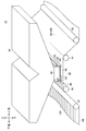
【解決手段】位相差板の製造方法は、互いに異なる方向に光学軸が配向された複数の領域が形成された配向パターンを有する位相差板の製造方法であって、基材の一面に光で配向する未配向の光配向層を配する工程と、前記位相差板の前記配向パターンの前記複数の領域に対応して、1/4波長板の位相差機能を有する複数の領域が形成された配向パターンを有する位相差マスクを準備する工程と、前記位相差マスクに楕円偏光を照射して、前記位相差マスクから出射した偏光を前記光配向層に照射することにより、前記光配向層を配向させる工程とを備える。
【選択図】図6
Description
[特許文献1] 特開平9−33914号公報
Claims (12)
- 互いに異なる方向に光学軸が配向された複数の領域が形成された配向パターンを有する位相差板の製造方法であって、
基材の一面に光で配向する未配向の光配向層を配する工程と、
前記位相差板の前記配向パターンの前記複数の領域に対応して、1/4波長板の位相差機能を有する複数の領域が形成された配向パターンを有する位相差マスクを準備する工程と、
前記位相差マスクに楕円偏光を照射して、前記位相差マスクから出射した偏光を前記光配向層に照射することにより、前記光配向層を配向させる工程と
を備える位相差板の製造方法。 - 前記位相差マスクの前記複数の領域の幅は、前記位相差板の前記複数の領域の幅と等しい
請求項1に記載の位相差板の製造方法。 - 前記位相差マスクの隣接する領域の光学軸間の角度差は、前記位相差板の隣接する領域の光学軸間の角度差と等しい請求項1または請求項2に記載の位相差板の製造方法。
- 前記位相差マスクは、前記配向パターンを保持するマスク基材を備え、
前記配向パターンは、配向膜及び液晶膜と、前記配向膜が形成される基材とを有し、
前記液晶膜が、前記光配向層側に配される
請求項1から請求項3のいずれか1項に記載の位相差板の製造方法。 - 前記位相差マスクの前記配向パターンの一面には、前記位相差マスクの前記配向パターンの酸化を防止する保護膜が形成されている
請求項1から請求項4のいずれか1項に記載の位相差板の製造方法。 - 前記楕円偏光は、紫外線である
請求項1から請求項5のいずれか1項に記載の位相差板の製造方法。 - 前記位相差マスクは、前記位相差マスクの前記配向パターンが形成された複数の位相差板が並べられた構成を有する
請求項1から請求項6のいずれか1項に記載の位相差板の製造方法。 - 互いに異なる方向に光学軸が配向された複数の領域が形成された配向パターンが繰り返された位相差板の製造方法であって、
基材の一面に光で配向する未配向の光配向層を配する工程と、
前記位相差板の前記配向パターンの前記複数の領域の少なくとも一部に対応する複数の領域が形成された配向パターンを有する位相差板を複数並べた位相差マスクを準備する工程と、
前記位相差マスクに偏光を照射して、前記位相差マスクから出射した偏光を前記光配向層に照射することにより、前記光配向層を配向させる工程と
を備える位相差板の製造方法。 - 前記光配向層を搬送する工程を更に備え、
前記位相差マスクは、異なる配向パターンが形成された位相差板を複数並べた第1マスク部材及び第2マスク部材を有し、
前記第1マスク部材と前記第2マスク部材は、前記光配向層の搬送方向において、異なる位置に配されている
請求項8に記載の位相差板の製造方法。 - 前記第1マスク部材及び前記第2マスク部材の前記配向パターンの各領域は、前記位相差板の前記配向パターンの各領域の幅よりも大きい
請求項9に記載の位相差板の製造方法。 - 前記偏光の照射方向から見て、前記第1マスク部材及び前記第2マスク部材の前記位相差板間の境界には、遮光膜が形成されている
請求項10に記載の位相差板の製造方法。 - 前記遮光膜よりも前記第1マスク部材及び前記第2マスク部材の前記配向パターンが、前記光配向層に近い位置に配される
請求項11に記載の位相差板の製造方法。
Priority Applications (6)
| Application Number | Priority Date | Filing Date | Title |
|---|---|---|---|
| JP2012070153A JP5922459B2 (ja) | 2012-03-26 | 2012-03-26 | 位相差板の製造方法 |
| CN201380014626.1A CN104246550B (zh) | 2012-03-26 | 2013-02-27 | 相移板的制造方法 |
| PCT/JP2013/001164 WO2013145550A1 (ja) | 2012-03-26 | 2013-02-27 | 位相差板の製造方法 |
| KR1020147025189A KR20140146584A (ko) | 2012-03-26 | 2013-02-27 | 위상차판의 제조방법 |
| TW102110409A TWI571659B (zh) | 2012-03-26 | 2013-03-25 | 相位差板的製造方法 |
| US14/492,076 US20150008601A1 (en) | 2012-03-26 | 2014-09-22 | Retardation plate manufacturing method |
Applications Claiming Priority (1)
| Application Number | Priority Date | Filing Date | Title |
|---|---|---|---|
| JP2012070153A JP5922459B2 (ja) | 2012-03-26 | 2012-03-26 | 位相差板の製造方法 |
Publications (2)
| Publication Number | Publication Date |
|---|---|
| JP2013200520A true JP2013200520A (ja) | 2013-10-03 |
| JP5922459B2 JP5922459B2 (ja) | 2016-05-24 |
Family
ID=49258874
Family Applications (1)
| Application Number | Title | Priority Date | Filing Date |
|---|---|---|---|
| JP2012070153A Active JP5922459B2 (ja) | 2012-03-26 | 2012-03-26 | 位相差板の製造方法 |
Country Status (6)
| Country | Link |
|---|---|
| US (1) | US20150008601A1 (ja) |
| JP (1) | JP5922459B2 (ja) |
| KR (1) | KR20140146584A (ja) |
| CN (1) | CN104246550B (ja) |
| TW (1) | TWI571659B (ja) |
| WO (1) | WO2013145550A1 (ja) |
Cited By (1)
| Publication number | Priority date | Publication date | Assignee | Title |
|---|---|---|---|---|
| WO2018225611A1 (ja) * | 2017-06-07 | 2018-12-13 | シャープ株式会社 | 液晶パネルの製造方法、及び、液晶パネル用基板の光配向処理装置 |
Families Citing this family (5)
| Publication number | Priority date | Publication date | Assignee | Title |
|---|---|---|---|---|
| WO2014064742A1 (ja) * | 2012-10-26 | 2014-05-01 | 株式会社有沢製作所 | 露光装置、マスク、及び、光学フィルム |
| EP4099084A4 (en) * | 2020-01-30 | 2024-02-21 | Nippon Kayaku Kabushiki Kaisha | OPTICAL FUNCTIONAL FILM FOR HEAD-UP DISPLAY, OPTICAL LAMINATE, FUNCTIONAL GLASS AND HEAD-UP DISPLAY SYSTEM |
| CN115066645B (zh) * | 2020-02-13 | 2026-03-17 | 中央玻璃产品株式会社 | 抬头显示装置、抬头显示系统 |
| US11716209B2 (en) * | 2020-04-14 | 2023-08-01 | The Regents Of The University Of Colorado, A Body Corporate | Systems and methods for azimuthal multiplexing three-dimensional diffractive optics |
| WO2022196732A1 (ja) * | 2021-03-19 | 2022-09-22 | 日本化薬株式会社 | ヘッドアップディスプレイ用光学機能フィルム、光学積層体、機能性ガラス、およびヘッドアップディスプレイシステム |
Citations (7)
| Publication number | Priority date | Publication date | Assignee | Title |
|---|---|---|---|---|
| JPH04366841A (ja) * | 1991-06-13 | 1992-12-18 | Nikon Corp | フォトマスク及びこれを用いた露光方法 |
| JPH0933914A (ja) * | 1995-07-11 | 1997-02-07 | F Hoffmann La Roche Ag | 偏光パターンを移動するための装置 |
| JP2004111500A (ja) * | 2002-09-17 | 2004-04-08 | Canon Inc | マスク、露光装置及び方法 |
| JP2006030568A (ja) * | 2004-07-15 | 2006-02-02 | Advanced Lcd Technologies Development Center Co Ltd | フォトマスク |
| JP2006293330A (ja) * | 2005-03-18 | 2006-10-26 | Advanced Lcd Technologies Development Center Co Ltd | フォトマスク、位相シフトマスク、露光装置 |
| JP2011186423A (ja) * | 2010-03-09 | 2011-09-22 | Arisawa Mfg Co Ltd | 光学素子部材、立体画像表示装置及び光学素子部材の製造方法 |
| WO2013039100A1 (ja) * | 2011-09-16 | 2013-03-21 | 株式会社ブイ・テクノロジー | フィルム露光装置 |
Family Cites Families (9)
| Publication number | Priority date | Publication date | Assignee | Title |
|---|---|---|---|---|
| JP3923062B2 (ja) * | 2004-08-02 | 2007-05-30 | 日東電工株式会社 | 液晶配向フィルムの製造方法、液晶配向フィルム、光学フィルムおよび画像表示装置 |
| US7608369B2 (en) * | 2005-03-18 | 2009-10-27 | Advanced Lcd Technologies Development Center Co., Ltd. | Photomask to which phase shift is applied and exposure apparatus |
| US8643822B2 (en) * | 2007-07-03 | 2014-02-04 | Jds Uniphase Corporation | Non-etched flat polarization-selective diffractive optical elements |
| WO2009122621A1 (ja) * | 2008-03-31 | 2009-10-08 | 凸版印刷株式会社 | 位相差板、その製造方法及び液晶表示装置 |
| JP5514738B2 (ja) * | 2008-12-19 | 2014-06-04 | 株式会社有沢製作所 | 液晶フィルタ、位相差板及び光学ローパスフィルタ |
| WO2010150693A1 (ja) * | 2009-06-25 | 2010-12-29 | チッソ株式会社 | 光配向した液晶性ポリイミドによる位相差膜及び光学素子 |
| JP5213843B2 (ja) * | 2009-12-25 | 2013-06-19 | 日東電工株式会社 | 立体映像表示用位相差板、偏光素子およびそれらの製造方法、ならびに立体映像表示装置 |
| JP2012014064A (ja) * | 2010-07-02 | 2012-01-19 | Dainippon Printing Co Ltd | 光配向膜の製造方法、位相差フィルムの製造方法、光配向膜製造システム、光配向膜及び位相差フィルム |
| JP2012018256A (ja) * | 2010-07-07 | 2012-01-26 | Hitachi High-Technologies Corp | 液晶用配向膜露光方法及びその装置 |
-
2012
- 2012-03-26 JP JP2012070153A patent/JP5922459B2/ja active Active
-
2013
- 2013-02-27 CN CN201380014626.1A patent/CN104246550B/zh not_active Expired - Fee Related
- 2013-02-27 KR KR1020147025189A patent/KR20140146584A/ko not_active Ceased
- 2013-02-27 WO PCT/JP2013/001164 patent/WO2013145550A1/ja not_active Ceased
- 2013-03-25 TW TW102110409A patent/TWI571659B/zh not_active IP Right Cessation
-
2014
- 2014-09-22 US US14/492,076 patent/US20150008601A1/en not_active Abandoned
Patent Citations (7)
| Publication number | Priority date | Publication date | Assignee | Title |
|---|---|---|---|---|
| JPH04366841A (ja) * | 1991-06-13 | 1992-12-18 | Nikon Corp | フォトマスク及びこれを用いた露光方法 |
| JPH0933914A (ja) * | 1995-07-11 | 1997-02-07 | F Hoffmann La Roche Ag | 偏光パターンを移動するための装置 |
| JP2004111500A (ja) * | 2002-09-17 | 2004-04-08 | Canon Inc | マスク、露光装置及び方法 |
| JP2006030568A (ja) * | 2004-07-15 | 2006-02-02 | Advanced Lcd Technologies Development Center Co Ltd | フォトマスク |
| JP2006293330A (ja) * | 2005-03-18 | 2006-10-26 | Advanced Lcd Technologies Development Center Co Ltd | フォトマスク、位相シフトマスク、露光装置 |
| JP2011186423A (ja) * | 2010-03-09 | 2011-09-22 | Arisawa Mfg Co Ltd | 光学素子部材、立体画像表示装置及び光学素子部材の製造方法 |
| WO2013039100A1 (ja) * | 2011-09-16 | 2013-03-21 | 株式会社ブイ・テクノロジー | フィルム露光装置 |
Cited By (1)
| Publication number | Priority date | Publication date | Assignee | Title |
|---|---|---|---|---|
| WO2018225611A1 (ja) * | 2017-06-07 | 2018-12-13 | シャープ株式会社 | 液晶パネルの製造方法、及び、液晶パネル用基板の光配向処理装置 |
Also Published As
| Publication number | Publication date |
|---|---|
| TWI571659B (zh) | 2017-02-21 |
| US20150008601A1 (en) | 2015-01-08 |
| TW201339665A (zh) | 2013-10-01 |
| JP5922459B2 (ja) | 2016-05-24 |
| CN104246550A (zh) | 2014-12-24 |
| KR20140146584A (ko) | 2014-12-26 |
| CN104246550B (zh) | 2017-04-05 |
| WO2013145550A1 (ja) | 2013-10-03 |
Similar Documents
| Publication | Publication Date | Title |
|---|---|---|
| JP5922459B2 (ja) | 位相差板の製造方法 | |
| JP5866028B2 (ja) | 露光装置、マスク、及び、光学フィルム | |
| TW201329587A (zh) | 光學膜製造裝置、光學膜的製造方法及光學膜 | |
| WO2012105178A1 (ja) | フィルム状製品の製造方法、フィルム状製品の製造装置、及び、マスク | |
| JP6776299B2 (ja) | 位相差フィルム及び光学積層体 | |
| JP2013254113A (ja) | 露光装置及び露光方法 | |
| CN116057433B (zh) | 光学各向异性层 | |
| JP6154750B2 (ja) | 光学フィルムの製造方法 | |
| CN116057431A (zh) | 光学各向异性层 | |
| JP7122168B2 (ja) | 接着層付き積層体、積層体、液晶層積層体、液晶フィルムの製造方法、及び、光学積層体の製造方法 | |
| JP2014199301A (ja) | メガネ用部材、メガネおよびメガネ用部材の製造方法 | |
| KR102248880B1 (ko) | 배향막, 편광판, 및 위상차판, 그 제조방법 및 제조장치 | |
| JP2019215471A (ja) | 光学積層体及びその製造方法 | |
| KR20130036911A (ko) | 패턴 리타더의 제조 방법 | |
| JP2014006364A (ja) | 露光装置及び露光方法 | |
| KR20110038854A (ko) | 패턴화 리타더의 제조장치와 제조방법 그리고 그 방법에 의하여 제조된 리타더 | |
| JP2019215584A (ja) | 光学積層体の製造方法 | |
| JP2019045845A (ja) | 光学積層体の製造方法及び複合偏光板の製造方法 | |
| JP2024046676A (ja) | 長尺位相差フィルム、長尺光学フィルム、長尺偏光フィルム、長尺位相差フィルムの製造方法、及び長尺光学フィルムの製造方法 | |
| KR20150144973A (ko) | 안경용 부재, 안경 및 안경용 부재의 제조방법 | |
| JP2024014147A (ja) | 長尺位相差フィルム、長尺光学フィルム、長尺偏光フィルム、長尺位相差フィルムの製造方法、及び長尺光学フィルムの製造方法 | |
| CN119563130A (zh) | 长条相位差膜、长条光学膜、长条偏光膜、长条相位差膜的制造方法以及长条光学膜的制造方法 | |
| JP2020060615A (ja) | 光学フィルム |
Legal Events
| Date | Code | Title | Description |
|---|---|---|---|
| A621 | Written request for application examination |
Free format text: JAPANESE INTERMEDIATE CODE: A621 Effective date: 20140926 |
|
| A131 | Notification of reasons for refusal |
Free format text: JAPANESE INTERMEDIATE CODE: A131 Effective date: 20150901 |
|
| A521 | Request for written amendment filed |
Free format text: JAPANESE INTERMEDIATE CODE: A523 Effective date: 20151028 |
|
| TRDD | Decision of grant or rejection written | ||
| A01 | Written decision to grant a patent or to grant a registration (utility model) |
Free format text: JAPANESE INTERMEDIATE CODE: A01 Effective date: 20160405 |
|
| A61 | First payment of annual fees (during grant procedure) |
Free format text: JAPANESE INTERMEDIATE CODE: A61 Effective date: 20160414 |
|
| R150 | Certificate of patent or registration of utility model |
Ref document number: 5922459 Country of ref document: JP Free format text: JAPANESE INTERMEDIATE CODE: R150 |
|
| R250 | Receipt of annual fees |
Free format text: JAPANESE INTERMEDIATE CODE: R250 |
|
| R250 | Receipt of annual fees |
Free format text: JAPANESE INTERMEDIATE CODE: R250 |
|
| R250 | Receipt of annual fees |
Free format text: JAPANESE INTERMEDIATE CODE: R250 |
|
| R250 | Receipt of annual fees |
Free format text: JAPANESE INTERMEDIATE CODE: R250 |
|
| R250 | Receipt of annual fees |
Free format text: JAPANESE INTERMEDIATE CODE: R250 |
|
| R250 | Receipt of annual fees |
Free format text: JAPANESE INTERMEDIATE CODE: R250 |
|
| R250 | Receipt of annual fees |
Free format text: JAPANESE INTERMEDIATE CODE: R250 |
|
| R250 | Receipt of annual fees |
Free format text: JAPANESE INTERMEDIATE CODE: R250 |