JP2015019088A - 光検出器 - Google Patents
光検出器 Download PDFInfo
- Publication number
- JP2015019088A JP2015019088A JP2014167511A JP2014167511A JP2015019088A JP 2015019088 A JP2015019088 A JP 2015019088A JP 2014167511 A JP2014167511 A JP 2014167511A JP 2014167511 A JP2014167511 A JP 2014167511A JP 2015019088 A JP2015019088 A JP 2015019088A
- Authority
- JP
- Japan
- Prior art keywords
- layer
- forming
- quantum structure
- doped
- doped layer
- Prior art date
- Legal status (The legal status is an assumption and is not a legal conclusion. Google has not performed a legal analysis and makes no representation as to the accuracy of the status listed.)
- Granted
Links
Images


Classifications
-
- H—ELECTRICITY
- H10—SEMICONDUCTOR DEVICES; ELECTRIC SOLID-STATE DEVICES NOT OTHERWISE PROVIDED FOR
- H10F—INORGANIC SEMICONDUCTOR DEVICES SENSITIVE TO INFRARED RADIATION, LIGHT, ELECTROMAGNETIC RADIATION OF SHORTER WAVELENGTH OR CORPUSCULAR RADIATION
- H10F77/00—Constructional details of devices covered by this subclass
- H10F77/10—Semiconductor bodies
- H10F77/14—Shape of semiconductor bodies; Shapes, relative sizes or dispositions of semiconductor regions within semiconductor bodies
- H10F77/143—Shape of semiconductor bodies; Shapes, relative sizes or dispositions of semiconductor regions within semiconductor bodies comprising quantum structures
-
- B—PERFORMING OPERATIONS; TRANSPORTING
- B82—NANOTECHNOLOGY
- B82Y—SPECIFIC USES OR APPLICATIONS OF NANOSTRUCTURES; MEASUREMENT OR ANALYSIS OF NANOSTRUCTURES; MANUFACTURE OR TREATMENT OF NANOSTRUCTURES
- B82Y20/00—Nanooptics, e.g. quantum optics or photonic crystals
-
- H—ELECTRICITY
- H10—SEMICONDUCTOR DEVICES; ELECTRIC SOLID-STATE DEVICES NOT OTHERWISE PROVIDED FOR
- H10F—INORGANIC SEMICONDUCTOR DEVICES SENSITIVE TO INFRARED RADIATION, LIGHT, ELECTROMAGNETIC RADIATION OF SHORTER WAVELENGTH OR CORPUSCULAR RADIATION
- H10F10/00—Individual photovoltaic cells, e.g. solar cells
- H10F10/10—Individual photovoltaic cells, e.g. solar cells having potential barriers
-
- H—ELECTRICITY
- H10—SEMICONDUCTOR DEVICES; ELECTRIC SOLID-STATE DEVICES NOT OTHERWISE PROVIDED FOR
- H10F—INORGANIC SEMICONDUCTOR DEVICES SENSITIVE TO INFRARED RADIATION, LIGHT, ELECTROMAGNETIC RADIATION OF SHORTER WAVELENGTH OR CORPUSCULAR RADIATION
- H10F30/00—Individual radiation-sensitive semiconductor devices in which radiation controls the flow of current through the devices, e.g. photodetectors
- H10F30/20—Individual radiation-sensitive semiconductor devices in which radiation controls the flow of current through the devices, e.g. photodetectors the devices having potential barriers, e.g. phototransistors
- H10F30/21—Individual radiation-sensitive semiconductor devices in which radiation controls the flow of current through the devices, e.g. photodetectors the devices having potential barriers, e.g. phototransistors the devices being sensitive to infrared, visible or ultraviolet radiation
-
- H—ELECTRICITY
- H10—SEMICONDUCTOR DEVICES; ELECTRIC SOLID-STATE DEVICES NOT OTHERWISE PROVIDED FOR
- H10F—INORGANIC SEMICONDUCTOR DEVICES SENSITIVE TO INFRARED RADIATION, LIGHT, ELECTROMAGNETIC RADIATION OF SHORTER WAVELENGTH OR CORPUSCULAR RADIATION
- H10F77/00—Constructional details of devices covered by this subclass
- H10F77/10—Semiconductor bodies
- H10F77/12—Active materials
- H10F77/123—Active materials comprising only Group II-VI materials, e.g. CdS, ZnS or HgCdTe
-
- H—ELECTRICITY
- H10—SEMICONDUCTOR DEVICES; ELECTRIC SOLID-STATE DEVICES NOT OTHERWISE PROVIDED FOR
- H10F—INORGANIC SEMICONDUCTOR DEVICES SENSITIVE TO INFRARED RADIATION, LIGHT, ELECTROMAGNETIC RADIATION OF SHORTER WAVELENGTH OR CORPUSCULAR RADIATION
- H10F77/00—Constructional details of devices covered by this subclass
- H10F77/10—Semiconductor bodies
- H10F77/14—Shape of semiconductor bodies; Shapes, relative sizes or dispositions of semiconductor regions within semiconductor bodies
- H10F77/146—Superlattices; Multiple quantum well structures
-
- H—ELECTRICITY
- H10—SEMICONDUCTOR DEVICES; ELECTRIC SOLID-STATE DEVICES NOT OTHERWISE PROVIDED FOR
- H10F—INORGANIC SEMICONDUCTOR DEVICES SENSITIVE TO INFRARED RADIATION, LIGHT, ELECTROMAGNETIC RADIATION OF SHORTER WAVELENGTH OR CORPUSCULAR RADIATION
- H10F77/00—Constructional details of devices covered by this subclass
- H10F77/40—Optical elements or arrangements
- H10F77/413—Optical elements or arrangements directly associated or integrated with the devices, e.g. back reflectors
-
- H—ELECTRICITY
- H10—SEMICONDUCTOR DEVICES; ELECTRIC SOLID-STATE DEVICES NOT OTHERWISE PROVIDED FOR
- H10P—GENERIC PROCESSES OR APPARATUS FOR THE MANUFACTURE OR TREATMENT OF DEVICES COVERED BY CLASS H10
- H10P14/00—Formation of materials, e.g. in the shape of layers or pillars
- H10P14/20—Formation of materials, e.g. in the shape of layers or pillars of semiconductor materials
- H10P14/34—Deposited materials, e.g. layers
- H10P14/3402—Deposited materials, e.g. layers characterised by the chemical composition
- H10P14/3424—Deposited materials, e.g. layers characterised by the chemical composition being Group IIB-VIA materials
- H10P14/3426—Oxides
-
- H—ELECTRICITY
- H10—SEMICONDUCTOR DEVICES; ELECTRIC SOLID-STATE DEVICES NOT OTHERWISE PROVIDED FOR
- H10P—GENERIC PROCESSES OR APPARATUS FOR THE MANUFACTURE OR TREATMENT OF DEVICES COVERED BY CLASS H10
- H10P14/00—Formation of materials, e.g. in the shape of layers or pillars
- H10P14/20—Formation of materials, e.g. in the shape of layers or pillars of semiconductor materials
- H10P14/34—Deposited materials, e.g. layers
- H10P14/3402—Deposited materials, e.g. layers characterised by the chemical composition
- H10P14/3424—Deposited materials, e.g. layers characterised by the chemical composition being Group IIB-VIA materials
- H10P14/3428—Sulfides
-
- H—ELECTRICITY
- H10—SEMICONDUCTOR DEVICES; ELECTRIC SOLID-STATE DEVICES NOT OTHERWISE PROVIDED FOR
- H10P—GENERIC PROCESSES OR APPARATUS FOR THE MANUFACTURE OR TREATMENT OF DEVICES COVERED BY CLASS H10
- H10P14/00—Formation of materials, e.g. in the shape of layers or pillars
- H10P14/20—Formation of materials, e.g. in the shape of layers or pillars of semiconductor materials
- H10P14/34—Deposited materials, e.g. layers
- H10P14/3402—Deposited materials, e.g. layers characterised by the chemical composition
- H10P14/3434—Deposited materials, e.g. layers characterised by the chemical composition being oxide semiconductor materials
-
- H—ELECTRICITY
- H10—SEMICONDUCTOR DEVICES; ELECTRIC SOLID-STATE DEVICES NOT OTHERWISE PROVIDED FOR
- H10P—GENERIC PROCESSES OR APPARATUS FOR THE MANUFACTURE OR TREATMENT OF DEVICES COVERED BY CLASS H10
- H10P14/00—Formation of materials, e.g. in the shape of layers or pillars
- H10P14/20—Formation of materials, e.g. in the shape of layers or pillars of semiconductor materials
- H10P14/34—Deposited materials, e.g. layers
- H10P14/3402—Deposited materials, e.g. layers characterised by the chemical composition
- H10P14/3436—Deposited materials, e.g. layers characterised by the chemical composition being chalcogenide semiconductor materials not being oxides, e.g. ternary compounds
-
- Y—GENERAL TAGGING OF NEW TECHNOLOGICAL DEVELOPMENTS; GENERAL TAGGING OF CROSS-SECTIONAL TECHNOLOGIES SPANNING OVER SEVERAL SECTIONS OF THE IPC; TECHNICAL SUBJECTS COVERED BY FORMER USPC CROSS-REFERENCE ART COLLECTIONS [XRACs] AND DIGESTS
- Y02—TECHNOLOGIES OR APPLICATIONS FOR MITIGATION OR ADAPTATION AGAINST CLIMATE CHANGE
- Y02E—REDUCTION OF GREENHOUSE GAS [GHG] EMISSIONS, RELATED TO ENERGY GENERATION, TRANSMISSION OR DISTRIBUTION
- Y02E10/00—Energy generation through renewable energy sources
- Y02E10/50—Photovoltaic [PV] energy
Landscapes
- Chemical & Material Sciences (AREA)
- Engineering & Computer Science (AREA)
- Nanotechnology (AREA)
- Physics & Mathematics (AREA)
- Life Sciences & Earth Sciences (AREA)
- Biophysics (AREA)
- Optics & Photonics (AREA)
- Crystallography & Structural Chemistry (AREA)
- Light Receiving Elements (AREA)
Abstract
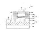
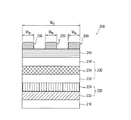
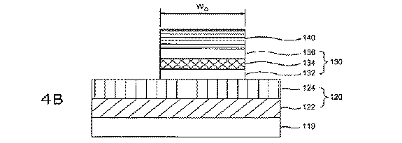
【解決手段】量子井戸検出器100の実装を提示する。量子構造130は、第1の障壁層132、第1の障壁層132上に配置される井戸層134、および井戸層134上に配置される第2の障壁層136を備える。金属層150は、この量子構造130に隣接して配置される。表面プラズモン共鳴による結合を利用して量子井戸検出器100の効率を高める。
【選択図】図1
Description
上の表1に示されているように、II−VI族半導体は、約1.5eVから約5.0eVまでの範囲のバンドギャップエネルギーを有する。例えば、井戸層134は、所定のスペクトルに対応するバンドギャップエネルギーを有するように、その成分が表1にリストされているII−VI族半導体のうちから選択される半導体化合物を含むことができる。六方晶構造を持つII−VI族半導体を含む化合物は、強い結合エネルギーを有することができ、これは量子効率を改善するうえで有利である。さらに、六方晶系II−VI族半導体は、立方晶系II−VI族半導体に比べて、高励起準位の下で、ダークスポットの形成に対して耐性があることが知られている。これは、六方晶構造は対称性の低い構造であり、デバイス内の欠陥の伝搬を抑制するからである。例えば、デバイス内で縮退故障が発生すると仮定する。デバイスが対称的な構造を有する場合、縮退故障は、対称構造内を容易に伝搬しうる。しかし、縮退故障は、伝搬せず、六方晶構造または他の非対称構造内のある点で停止しうる。障壁層132、136は、電子または正孔などのキャリアが井戸層134内に閉じ込められるようなエネルギーバンドを有するように構成されうる。一実施形態では、障壁層132、136は、井戸層134内に電子を閉じ込めるために井戸層134の伝導帯より高い伝導帯を有することができる。一実施形態では、障壁層132、136は、井戸層134内に正孔を閉じ込めるために井戸層134の価電子帯より低い価電子帯を有することができる。
[式1]
Eg=3.723−1.241xeV
式1によれば、x=0.7の場合、CdxZn1−xSのバンドギャップエネルギーEgは、2.853eVであり、これは435nmの波長(例えば、青色スペクトル)に対応する。井戸層134内に見られるCdxZn1−xSのXは、青色スペクトル検出のためには、約0.5から1までの範囲とすることができる。一実施形態では、障壁層132、136は、井戸層134がCdZnSを含む場合、ZnS、MgZnS、およびCdMgZnSのうちの1つを含むものとしてもよい。
[式2]
式中、Dxはx軸にそった電気変位場であり、Exはx軸にそった電場の強さであり、εは誘電率である。
Claims (23)
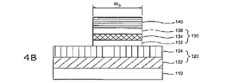
- 第1の障壁層、
前記第1の障壁層上に配置された井戸層、および
前記井戸層上に配置された第2の障壁層を備える量子構造と、
前記量子構造に隣接して配置される金属層と
を備えるデバイス。 - 前記量子構造は、II−VI族半導体を含む請求項1に記載のデバイス。
- 前記II−VI族半導体は、六方晶構造である請求項2に記載のデバイス。
- 前記井戸層は、xを約0.5から約1までの範囲とするCdxZn1−xSを含む請求項1に記載のデバイス。
- 前記第1の障壁層および前記第2の障壁層が、本質的にZnS、MgZnS、MgCdZnS、ZnO、MgZnO、およびMgCdZnOからなる群から選択された半導体を含む請求項1に記載のデバイス。
- 前記量子構造は、約100nm未満の幅を有し、前記金属層は、約100nm未満の幅を有する請求項1に記載のデバイス。
- 前記金属層は、本質的にAg、Al、Au、Ni、およびTiからなる群から選択された金属材料を含む請求項1に記載のデバイス。
- 前記第1の障壁層の下に配置された第1のドープ層と、
前記第2の障壁層上に配置された第2のドープ層とをさらに備え、
前記金属層は、前記第1のドープ層上に、かつ前記第2のドープ層に隣接して配置される請求項1に記載のデバイス。 - 前記第1のドープ層の下に配置された基材をさらに備える請求項8に記載のデバイス。
- 前記基材は、GaAsを含む請求項9に記載のデバイス。
- 前記金属層は、前記量子構造の両側部に沿って隣接する請求項1に記載のデバイス。
- 前記井戸層は、サブバンド上に電子を有し、該サブバンド間の1つまたは複数の遷移が青色スペクトルを持つ光子に対応する請求項1に記載のデバイス。
- 前記金属層は、前記量子構造上に配置され、前記金属層は、前記量子構造の幅より小さい幅を有する請求項1に記載のデバイス。
- 前記第1の障壁層の下に配置された第1のドープ層と、
前記第2の障壁層上に配置された第2のドープ層とをさらに備え、
前記金属層は、前記第2のドープ層上に配置されている請求項13に記載のデバイス。 - 2つまたはそれ以上の金属層が前記量子構造上に配置されてグレーティング構造を形成し、前記2つまたはそれ以上の金属層の幅の合計は、前記量子構造の前記幅より小さい請求項13に記載のデバイス。
- 第1の障壁層を形成すること、
前記第1の障壁層上に井戸層を形成すること、及び
前記井戸層上に第2の障壁層を形成すること
によって量子構造を形成すること、
前記量子構造が所定の幅を有するようになるまで前記量子構造の一部を取り除くこと、および
前記量子構造に隣接する位置に金属層を形成することを含む方法。 - 第1のドープ層を形成すること、および
第2のドープ層を前記第2の障壁層上に形成することをさらに含む請求項16に記載の方法であって、
第1の障壁層を形成することは、第1の障壁層を前記第1のドープ層上に形成することを含み、
前記量子構造の一部を取り除くことは、前記第2のドープ層が前記量子構造と同じ幅を有するように前記第2のドープ層に対応する前記量子構造の一部を取り除くことをさらに含み、
金属層を形成することは、金属層を前記第1のドープ層上に、前記量子構造及び前記第2のドープ層に隣接するように形成することをさらに含む方法。 - 基材を用意することをさらに含み、
前記第1のドープ層を形成することは、前記第1のドープ層を前記基材上に形成することを含む請求項17に記載の方法。 - 前記金属層を形成することは、前記量子構造の両側部に沿って隣接する金属層を形成すること含む請求項16に記載の方法。
- 前記井戸層は、サブバンド上に電子を有し、該サブバンド間の1つまたは複数の遷移は青色スペクトルを持つ光子に対応する請求項16に記載の方法。
- 第1の障壁層を形成すること、
前記第1の障壁層上に井戸層を形成すること、及び
前記井戸層上に第2の障壁層を形成すること
によって量子構造を形成すること、および
前記量子構造上に金属層を形成することを含み、
前記金属層は、前記量子構造の幅より小さい幅を有する方法。 - 第1のドープ層を形成すること、および
第2のドープ層を前記第2の障壁層上に形成することをさらに含む請求項21に記載の方法であって、
第1の障壁層を形成することは、第1の障壁層を前記第1のドープ層上に形成することを含み、
前記金属層を形成することは、金属層を前記第2のドープ層上に形成することをさらに含む請求項21に記載の方法。 - 前記金属層を形成することは、2つまたはそれ以上の金属層をグレーティングの形態で前記量子構造上に形成することをさらに含み、
前記2つまたはそれ以上の金属層の幅の合計は、前記量子構造の前記幅より小さい請求項21に記載の方法。
Applications Claiming Priority (2)
| Application Number | Priority Date | Filing Date | Title |
|---|---|---|---|
| US12/472,168 | 2009-05-26 | ||
| US12/472,168 US8373153B2 (en) | 2009-05-26 | 2009-05-26 | Photodetectors |
Related Parent Applications (1)
| Application Number | Title | Priority Date | Filing Date |
|---|---|---|---|
| JP2012512967A Division JP2012528481A (ja) | 2009-05-26 | 2010-05-26 | 光検出器 |
Publications (2)
| Publication Number | Publication Date |
|---|---|
| JP2015019088A true JP2015019088A (ja) | 2015-01-29 |
| JP5984885B2 JP5984885B2 (ja) | 2016-09-06 |
Family
ID=43219201
Family Applications (2)
| Application Number | Title | Priority Date | Filing Date |
|---|---|---|---|
| JP2012512967A Pending JP2012528481A (ja) | 2009-05-26 | 2010-05-26 | 光検出器 |
| JP2014167511A Expired - Fee Related JP5984885B2 (ja) | 2009-05-26 | 2014-08-20 | 光検出器 |
Family Applications Before (1)
| Application Number | Title | Priority Date | Filing Date |
|---|---|---|---|
| JP2012512967A Pending JP2012528481A (ja) | 2009-05-26 | 2010-05-26 | 光検出器 |
Country Status (5)
| Country | Link |
|---|---|
| US (1) | US8373153B2 (ja) |
| JP (2) | JP2012528481A (ja) |
| KR (1) | KR101355983B1 (ja) |
| DE (1) | DE112010002092A5 (ja) |
| WO (1) | WO2010137865A1 (ja) |
Families Citing this family (20)
| Publication number | Priority date | Publication date | Assignee | Title |
|---|---|---|---|---|
| FR2940522B1 (fr) * | 2008-12-24 | 2011-03-18 | Commissariat Energie Atomique | Photodetecteur comprenant une region semiconductrice tres mince |
| US8373153B2 (en) | 2009-05-26 | 2013-02-12 | University Of Seoul Industry Cooperation Foundation | Photodetectors |
| US8367925B2 (en) * | 2009-06-29 | 2013-02-05 | University Of Seoul Industry Cooperation Foundation | Light-electricity conversion device |
| US8395141B2 (en) | 2009-07-06 | 2013-03-12 | University Of Seoul Industry Cooperation Foundation | Compound semiconductors |
| US8748862B2 (en) * | 2009-07-06 | 2014-06-10 | University Of Seoul Industry Cooperation Foundation | Compound semiconductors |
| JP5374643B2 (ja) * | 2009-07-06 | 2013-12-25 | ユニバーシティ オブ ソウル インダストリー コーポレーション ファウンデーション | 長波長放射を検出することができる光検出器 |
| US8227793B2 (en) * | 2009-07-06 | 2012-07-24 | University Of Seoul Industry Cooperation Foundation | Photodetector capable of detecting the visible light spectrum |
| US8809834B2 (en) | 2009-07-06 | 2014-08-19 | University Of Seoul Industry Cooperation Foundation | Photodetector capable of detecting long wavelength radiation |
| US8368990B2 (en) | 2009-08-21 | 2013-02-05 | University Of Seoul Industry Cooperation Foundation | Polariton mode optical switch with composite structure |
| US8368047B2 (en) * | 2009-10-27 | 2013-02-05 | University Of Seoul Industry Cooperation Foundation | Semiconductor device |
| JP5899519B2 (ja) * | 2009-11-05 | 2016-04-06 | パナソニックIpマネジメント株式会社 | 固体撮像装置 |
| US8058641B2 (en) | 2009-11-18 | 2011-11-15 | University of Seoul Industry Corporation Foundation | Copper blend I-VII compound semiconductor light-emitting devices |
| CN103367518A (zh) * | 2012-03-31 | 2013-10-23 | 中国科学院上海微系统与信息技术研究所 | 一种表面等离激元耦合太赫兹量子阱探测器 |
| RU2510101C2 (ru) * | 2012-06-07 | 2014-03-20 | Федеральное государственное бюджетное учреждение науки Институт физики микроструктур Российской академии наук | Фоточувствительная структура и селективное фотоприемное устройство на ее основе |
| US9698286B2 (en) * | 2013-02-20 | 2017-07-04 | The Research Foundation Of The City University Of New York | Quantum well infrared photodetectors using II-VI material systems |
| US9231131B2 (en) | 2014-01-07 | 2016-01-05 | International Business Machines Corporation | Integrated photodetector waveguide structure with alignment tolerance |
| WO2016191142A2 (en) | 2015-05-27 | 2016-12-01 | Verily Life Sciences Llc | Nanophotonic hyperspectral/lightfield superpixel imager |
| CN110164994B (zh) * | 2018-03-16 | 2021-04-09 | 北京纳米能源与系统研究所 | InGaN/GaN多量子阱太阳能电池 |
| CN111048604B (zh) * | 2019-12-17 | 2021-04-06 | 吉林大学 | 一种基于MgZnO/ZnSⅡ型异质结的紫外探测器及其制备方法 |
| US12468074B2 (en) * | 2023-12-20 | 2025-11-11 | Toyota Motor Engineering & Manufacturing North America, Inc. | Plasmonic borophene nanoribbon metal-insulator-metal structure for quantum imaging |
Citations (8)
| Publication number | Priority date | Publication date | Assignee | Title |
|---|---|---|---|---|
| JPH03108379A (ja) * | 1989-09-22 | 1991-05-08 | Nec Corp | 光伝導型赤外線検出器 |
| JPH03248479A (ja) * | 1990-02-26 | 1991-11-06 | Canon Inc | 光検出器 |
| JPH06196745A (ja) * | 1992-12-24 | 1994-07-15 | Nec Corp | 赤外線検出器 |
| JPH07133200A (ja) * | 1993-11-04 | 1995-05-23 | Asahi Chem Ind Co Ltd | 金属カルコゲナイド化合物超格子の製造方法 |
| JPH08264821A (ja) * | 1995-03-27 | 1996-10-11 | Agency Of Ind Science & Technol | 光電変換方法および光電変換素子 |
| JPH10509806A (ja) * | 1994-08-12 | 1998-09-22 | ブラント・エイ・ペインター,ザ・サード | 光電子カプラ |
| JP2000138420A (ja) * | 1998-07-29 | 2000-05-16 | Lucent Technol Inc | 半導体レ―ザ |
| WO2008075542A1 (ja) * | 2006-12-20 | 2008-06-26 | Nec Corporation | フォトダイオード、光通信デバイスおよび光インタコネクションモジュール |
Family Cites Families (75)
| Publication number | Priority date | Publication date | Assignee | Title |
|---|---|---|---|---|
| JPS5235999B2 (ja) | 1974-08-26 | 1977-09-12 | ||
| US4764261A (en) | 1986-10-31 | 1988-08-16 | Stemcor Corporation | Method of making improved photovoltaic heterojunction structures |
| US5175739A (en) | 1988-09-09 | 1992-12-29 | Fujitsu Limited | Semiconductor optical device having a non-linear operational characteristic |
| US5112410A (en) | 1989-06-27 | 1992-05-12 | The Boeing Company | Cadmium zinc sulfide by solution growth |
| JPH0410669A (ja) * | 1990-04-27 | 1992-01-14 | Mitsubishi Electric Corp | 半導体装置 |
| US5181221A (en) | 1990-09-12 | 1993-01-19 | Seiko Epson Corporation | Surface emission type semiconductor laser |
| US5317584A (en) | 1990-09-12 | 1994-05-31 | Seiko Epson Corporation | Surface emission type semiconductor laser |
| US5295148A (en) | 1990-09-12 | 1994-03-15 | Seiko Epson Corporation | Surface emission type semiconductor laser |
| US5404369A (en) | 1990-09-12 | 1995-04-04 | Seiko Epson Corporation | Surface emission type semiconductor laser |
| US5181757A (en) * | 1990-10-04 | 1993-01-26 | Montoya Arturo T | Plastic bag carrier |
| US5079774A (en) | 1990-12-27 | 1992-01-07 | International Business Machines Corporation | Polarization-tunable optoelectronic devices |
| US5404027A (en) | 1991-05-15 | 1995-04-04 | Minnesota Mining & Manufacturing Compay | Buried ridge II-VI laser diode |
| US5291507A (en) | 1991-05-15 | 1994-03-01 | Minnesota Mining And Manufacturing Company | Blue-green laser diode |
| US5427716A (en) | 1991-06-05 | 1995-06-27 | Matsushita Electric Industrial Co., Ltd. | Compound semiconductors and semiconductor light-emitting devices using the same |
| DE69217344T2 (de) | 1991-12-16 | 1997-08-21 | Ibm | Abstimmbarer Laser mit gekoppelter Quantumwell-Struktur |
| US5818072A (en) | 1992-05-12 | 1998-10-06 | North Carolina State University | Integrated heterostructure of group II-VI semiconductor materials including epitaxial ohmic contact and method of fabricating same |
| JP3227661B2 (ja) | 1993-09-28 | 2001-11-12 | キヤノン株式会社 | 歪量子井戸構造素子及びそれを有する光デバイス |
| JP2874570B2 (ja) * | 1993-12-20 | 1999-03-24 | 日本電気株式会社 | 半導体装置およびその製造方法 |
| JPH07202340A (ja) | 1993-12-28 | 1995-08-04 | Sharp Corp | 可視光半導体レーザ |
| US5646419A (en) | 1995-04-07 | 1997-07-08 | California Institute Of Technology | n-type wide bandgap semiconductors grown on a p-type layer to form hole injection pn heterojunctions and methods of fabricating the same |
| FR2734094B1 (fr) | 1995-05-12 | 1997-06-06 | Commissariat Energie Atomique | Emetteur infrarouge monolithique a semi-conducteur pompe par un microlaser solide declenche |
| JP3056062B2 (ja) | 1996-01-16 | 2000-06-26 | 日本電気株式会社 | 半導体発光素子 |
| US6542526B1 (en) | 1996-10-30 | 2003-04-01 | Hitachi, Ltd. | Optical information processor and semiconductor light emitting device suitable for the same |
| JP3282174B2 (ja) * | 1997-01-29 | 2002-05-13 | 日亜化学工業株式会社 | 窒化物半導体発光素子 |
| JPH10303452A (ja) * | 1997-04-25 | 1998-11-13 | Matsushita Electric Ind Co Ltd | 半導体光検出素子、半導体光変調素子及び光通信用送信装置 |
| US6069380A (en) | 1997-07-25 | 2000-05-30 | Regents Of The University Of Minnesota | Single-electron floating-gate MOS memory |
| JP4252665B2 (ja) | 1999-04-08 | 2009-04-08 | アイファイヤー アイピー コーポレイション | El素子 |
| JP4029420B2 (ja) | 1999-07-15 | 2008-01-09 | 独立行政法人科学技術振興機構 | ミリ波・遠赤外光検出器 |
| US6515313B1 (en) | 1999-12-02 | 2003-02-04 | Cree Lighting Company | High efficiency light emitters with reduced polarization-induced charges |
| US6803596B2 (en) | 1999-12-27 | 2004-10-12 | Sanyo Electric Co., Ltd. | Light emitting device |
| JP3817580B2 (ja) | 2000-08-18 | 2006-09-06 | 独立行政法人科学技術振興機構 | 励起子ポラリトン光スイッチ |
| WO2002084829A1 (en) | 2001-04-11 | 2002-10-24 | Cielo Communications, Inc. | Long wavelength vertical cavity surface emitting laser |
| WO2004006393A2 (en) | 2002-07-06 | 2004-01-15 | Optical Communication Products, Inc. | Method of self-aligning an oxide aperture with an annular intra-cavity contact in a long wavelength vcsel |
| US7135728B2 (en) | 2002-09-30 | 2006-11-14 | Nanosys, Inc. | Large-area nanoenabled macroelectronic substrates and uses therefor |
| US6936486B2 (en) * | 2002-11-19 | 2005-08-30 | Jdsu Uniphase Corporation | Low voltage multi-junction vertical cavity surface emitting laser |
| US7095058B2 (en) | 2003-03-21 | 2006-08-22 | Intel Corporation | System and method for an improved light-emitting device |
| US7227196B2 (en) | 2003-05-20 | 2007-06-05 | Burgener Ii Robert H | Group II-VI semiconductor devices |
| JP4669213B2 (ja) | 2003-08-29 | 2011-04-13 | 独立行政法人科学技術振興機構 | 電界効果トランジスタ及び単一電子トランジスタ並びにそれを用いたセンサ |
| US7052757B2 (en) | 2003-10-03 | 2006-05-30 | Hewlett-Packard Development Company, L.P. | Capping layer for enhanced performance media |
| US20050285128A1 (en) | 2004-02-10 | 2005-12-29 | California Institute Of Technology | Surface plasmon light emitter structure and method of manufacture |
| US7076138B2 (en) | 2004-02-20 | 2006-07-11 | Altair Center, Llc | Nanophotonic devices based on quantum systems embedded in frequency bandgap media |
| US7638817B2 (en) | 2004-04-26 | 2009-12-29 | Sensor Electronic Technology, Inc. | Device and method for managing radiation |
| JP4982729B2 (ja) * | 2005-01-27 | 2012-07-25 | 国立大学法人北海道大学 | 超高感度画像検出装置およびその製造方法、検出方法 |
| US7425732B2 (en) | 2005-04-27 | 2008-09-16 | Matsushita Electric Industrial Co., Ltd. | Nitride semiconductor device |
| US7420225B1 (en) | 2005-11-30 | 2008-09-02 | Sandia Corporation | Direct detector for terahertz radiation |
| JP2007158119A (ja) | 2005-12-06 | 2007-06-21 | Canon Inc | ナノワイヤを有する電気素子およびその製造方法並びに電気素子集合体 |
| US20070126021A1 (en) * | 2005-12-06 | 2007-06-07 | Yungryel Ryu | Metal oxide semiconductor film structures and methods |
| US20070298551A1 (en) | 2006-02-10 | 2007-12-27 | Ecole Polytechnique Federale De Lausanne (Epfl) | Fabrication of silicon nano wires and gate-all-around MOS devices |
| EP1989737A4 (en) | 2006-02-17 | 2010-03-17 | Ravenbrick Llc | QUANTUM DOT CONTROL DEVICE |
| KR100771772B1 (ko) | 2006-08-25 | 2007-10-30 | 삼성전기주식회사 | 백색 led 모듈 |
| JP4829046B2 (ja) * | 2006-08-30 | 2011-11-30 | 国立大学法人 名古屋工業大学 | 硫化金属ナノ粒子の製造方法及び光電変換素子 |
| US8258047B2 (en) | 2006-12-04 | 2012-09-04 | General Electric Company | Nanostructures, methods of depositing nanostructures and devices incorporating the same |
| US8183656B2 (en) * | 2006-12-14 | 2012-05-22 | Nec Corporation | Photodiode |
| JP4271239B2 (ja) * | 2007-01-05 | 2009-06-03 | 株式会社東芝 | レーザ誘導光配線装置 |
| US7989153B2 (en) | 2007-07-11 | 2011-08-02 | Qd Vision, Inc. | Method and apparatus for selectively patterning free standing quantum DOT (FSQDT) polymer composites |
| WO2009012345A2 (en) | 2007-07-16 | 2009-01-22 | Ascent Solar Technologies, Inc. | Hybrid multi-junction photovoltaic cells and associated methods |
| JP2009104420A (ja) | 2007-10-23 | 2009-05-14 | Hitachi Ltd | 記憶制御装置及び記憶装置の障害検出方法 |
| TWI363440B (en) * | 2007-11-01 | 2012-05-01 | Univ Nat Taiwan | Light-emitting device, light-emitting diode and method for forming a light-emitting device |
| KR20090047977A (ko) | 2007-11-09 | 2009-05-13 | 삼성전자주식회사 | 무기 발광 소자 |
| US20100301454A1 (en) | 2007-11-20 | 2010-12-02 | Yong-Hang Zhang | Lattice matched multi-junction photovoltaic and optoelectronic devices |
| GB2458443A (en) | 2008-02-29 | 2009-09-23 | Univ Dublin City | Electroluminescent device |
| WO2009120721A2 (en) | 2008-03-24 | 2009-10-01 | California Institute Of Technology | Plasmostor: a-metal-oxide-si field effect plasmonic modulator |
| JP2011517099A (ja) | 2008-04-04 | 2011-05-26 | ザ リージェンツ オブ ザ ユニバーシティ オブ カリフォルニア | プレーナー半極性(Al,In,Ga,B)Nベースの発光ダイオード向けMOCVD成長技術 |
| US8912428B2 (en) | 2008-10-22 | 2014-12-16 | Epir Technologies, Inc. | High efficiency multijunction II-VI photovoltaic solar cells |
| US8063396B2 (en) | 2009-04-30 | 2011-11-22 | University Of Seoul Industry Cooperation Foundation | Polariton mode optical switch |
| US8373153B2 (en) | 2009-05-26 | 2013-02-12 | University Of Seoul Industry Cooperation Foundation | Photodetectors |
| US8367925B2 (en) | 2009-06-29 | 2013-02-05 | University Of Seoul Industry Cooperation Foundation | Light-electricity conversion device |
| JP5374643B2 (ja) | 2009-07-06 | 2013-12-25 | ユニバーシティ オブ ソウル インダストリー コーポレーション ファウンデーション | 長波長放射を検出することができる光検出器 |
| US8227793B2 (en) | 2009-07-06 | 2012-07-24 | University Of Seoul Industry Cooperation Foundation | Photodetector capable of detecting the visible light spectrum |
| US8809834B2 (en) | 2009-07-06 | 2014-08-19 | University Of Seoul Industry Cooperation Foundation | Photodetector capable of detecting long wavelength radiation |
| US8748862B2 (en) | 2009-07-06 | 2014-06-10 | University Of Seoul Industry Cooperation Foundation | Compound semiconductors |
| US8395141B2 (en) | 2009-07-06 | 2013-03-12 | University Of Seoul Industry Cooperation Foundation | Compound semiconductors |
| US8368990B2 (en) | 2009-08-21 | 2013-02-05 | University Of Seoul Industry Cooperation Foundation | Polariton mode optical switch with composite structure |
| US8368047B2 (en) | 2009-10-27 | 2013-02-05 | University Of Seoul Industry Cooperation Foundation | Semiconductor device |
| US8058641B2 (en) | 2009-11-18 | 2011-11-15 | University of Seoul Industry Corporation Foundation | Copper blend I-VII compound semiconductor light-emitting devices |
-
2009
- 2009-05-26 US US12/472,168 patent/US8373153B2/en active Active
-
2010
- 2010-05-26 KR KR1020117030713A patent/KR101355983B1/ko active Active
- 2010-05-26 JP JP2012512967A patent/JP2012528481A/ja active Pending
- 2010-05-26 WO PCT/KR2010/003322 patent/WO2010137865A1/en not_active Ceased
- 2010-05-26 DE DE112010002092T patent/DE112010002092A5/de not_active Withdrawn
-
2014
- 2014-08-20 JP JP2014167511A patent/JP5984885B2/ja not_active Expired - Fee Related
Patent Citations (8)
| Publication number | Priority date | Publication date | Assignee | Title |
|---|---|---|---|---|
| JPH03108379A (ja) * | 1989-09-22 | 1991-05-08 | Nec Corp | 光伝導型赤外線検出器 |
| JPH03248479A (ja) * | 1990-02-26 | 1991-11-06 | Canon Inc | 光検出器 |
| JPH06196745A (ja) * | 1992-12-24 | 1994-07-15 | Nec Corp | 赤外線検出器 |
| JPH07133200A (ja) * | 1993-11-04 | 1995-05-23 | Asahi Chem Ind Co Ltd | 金属カルコゲナイド化合物超格子の製造方法 |
| JPH10509806A (ja) * | 1994-08-12 | 1998-09-22 | ブラント・エイ・ペインター,ザ・サード | 光電子カプラ |
| JPH08264821A (ja) * | 1995-03-27 | 1996-10-11 | Agency Of Ind Science & Technol | 光電変換方法および光電変換素子 |
| JP2000138420A (ja) * | 1998-07-29 | 2000-05-16 | Lucent Technol Inc | 半導体レ―ザ |
| WO2008075542A1 (ja) * | 2006-12-20 | 2008-06-26 | Nec Corporation | フォトダイオード、光通信デバイスおよび光インタコネクションモジュール |
Also Published As
| Publication number | Publication date |
|---|---|
| JP2012528481A (ja) | 2012-11-12 |
| KR20120024827A (ko) | 2012-03-14 |
| US20100301308A1 (en) | 2010-12-02 |
| DE112010002092A5 (de) | 2012-04-26 |
| DE112010002092T5 (de) | 2017-09-28 |
| JP5984885B2 (ja) | 2016-09-06 |
| US8373153B2 (en) | 2013-02-12 |
| WO2010137865A1 (en) | 2010-12-02 |
| KR101355983B1 (ko) | 2014-01-29 |
Similar Documents
| Publication | Publication Date | Title |
|---|---|---|
| JP5984885B2 (ja) | 光検出器 | |
| US8227793B2 (en) | Photodetector capable of detecting the visible light spectrum | |
| US8247790B2 (en) | White light emitting device | |
| US7964882B2 (en) | Nitride semiconductor-based light emitting devices | |
| CN101971367B (zh) | 红外线发光元件 | |
| Ren et al. | Solar-blind photodetector based on single crystal Ga2O3 film prepared by a unique ion-cutting process | |
| TW201501279A (zh) | 半導體元件及其製造方法 | |
| US20050012113A1 (en) | [uv photodetector] | |
| US8106421B2 (en) | Photovoltaic devices | |
| CN115004390A (zh) | 第iii族氮化物激子异质结构 | |
| US20110291108A1 (en) | Semiconductor photodetector with transparent interface charge control layer and method thereof | |
| CN102804411A (zh) | 利用铟耗尽机理在含铟衬底上生长的半导体器件 | |
| Reddy et al. | Large‐Area, Solar‐Blind, Sub‐250 nm Detection AlGaN Avalanche Photodiodes Grown on AlN Substrates | |
| CN113994487B (zh) | 半导体光器件的制造方法和半导体光器件 | |
| Mosca et al. | Multilayer (Al, Ga) N structures for solar-blind detection | |
| KR102099440B1 (ko) | 발광 소자의 제조 방법 | |
| WO2017042368A1 (en) | Semiconductor device having an internal-field-guarded active region | |
| KR101459770B1 (ko) | 그룹 3족 질화물계 반도체 소자 | |
| JP6755506B2 (ja) | 窒化物半導体発光素子及びその製造方法 | |
| US20100270547A1 (en) | Semiconductor device | |
| JP2015035550A (ja) | 半導体素子およびその製造方法 | |
| TWI899596B (zh) | 半導體發光元件和半導體發光元件的製造方法 | |
| CN108574004A (zh) | 具有内场防护有源区的半导体器件 | |
| KR100698387B1 (ko) | 중성빔 식각장치를 이용한 질화물 반도체 발광 소자 및 그제조 방법 | |
| WO2008069422A1 (en) | Nitride semiconductor-based light emitting devices |
Legal Events
| Date | Code | Title | Description |
|---|---|---|---|
| A977 | Report on retrieval |
Free format text: JAPANESE INTERMEDIATE CODE: A971007 Effective date: 20150527 |
|
| A131 | Notification of reasons for refusal |
Free format text: JAPANESE INTERMEDIATE CODE: A131 Effective date: 20150612 |
|
| A521 | Request for written amendment filed |
Free format text: JAPANESE INTERMEDIATE CODE: A523 Effective date: 20150910 |
|
| A131 | Notification of reasons for refusal |
Free format text: JAPANESE INTERMEDIATE CODE: A131 Effective date: 20160203 |
|
| A521 | Request for written amendment filed |
Free format text: JAPANESE INTERMEDIATE CODE: A523 Effective date: 20160426 |
|
| TRDD | Decision of grant or rejection written | ||
| A01 | Written decision to grant a patent or to grant a registration (utility model) |
Free format text: JAPANESE INTERMEDIATE CODE: A01 Effective date: 20160704 |
|
| A61 | First payment of annual fees (during grant procedure) |
Free format text: JAPANESE INTERMEDIATE CODE: A61 Effective date: 20160802 |
|
| R150 | Certificate of patent or registration of utility model |
Ref document number: 5984885 Country of ref document: JP Free format text: JAPANESE INTERMEDIATE CODE: R150 |
|
| LAPS | Cancellation because of no payment of annual fees |