JP2015228014A - 表示装置および、その動作方法 - Google Patents
表示装置および、その動作方法 Download PDFInfo
- Publication number
- JP2015228014A JP2015228014A JP2015084176A JP2015084176A JP2015228014A JP 2015228014 A JP2015228014 A JP 2015228014A JP 2015084176 A JP2015084176 A JP 2015084176A JP 2015084176 A JP2015084176 A JP 2015084176A JP 2015228014 A JP2015228014 A JP 2015228014A
- Authority
- JP
- Japan
- Prior art keywords
- circuit
- substrate
- display device
- display
- oxide semiconductor
- Prior art date
- Legal status (The legal status is an assumption and is not a legal conclusion. Google has not performed a legal analysis and makes no representation as to the accuracy of the status listed.)
- Granted
Links
Images









Classifications
-
- G—PHYSICS
- G06—COMPUTING OR CALCULATING; COUNTING
- G06F—ELECTRIC DIGITAL DATA PROCESSING
- G06F3/00—Input arrangements for transferring data to be processed into a form capable of being handled by the computer; Output arrangements for transferring data from processing unit to output unit, e.g. interface arrangements
- G06F3/01—Input arrangements or combined input and output arrangements for interaction between user and computer
- G06F3/03—Arrangements for converting the position or the displacement of a member into a coded form
- G06F3/041—Digitisers, e.g. for touch screens or touch pads, characterised by the transducing means
- G06F3/0412—Digitisers structurally integrated in a display
-
- G—PHYSICS
- G06—COMPUTING OR CALCULATING; COUNTING
- G06F—ELECTRIC DIGITAL DATA PROCESSING
- G06F3/00—Input arrangements for transferring data to be processed into a form capable of being handled by the computer; Output arrangements for transferring data from processing unit to output unit, e.g. interface arrangements
- G06F3/01—Input arrangements or combined input and output arrangements for interaction between user and computer
- G06F3/03—Arrangements for converting the position or the displacement of a member into a coded form
- G06F3/041—Digitisers, e.g. for touch screens or touch pads, characterised by the transducing means
- G06F3/0416—Control or interface arrangements specially adapted for digitisers
- G06F3/0418—Control or interface arrangements specially adapted for digitisers for error correction or compensation, e.g. based on parallax, calibration or alignment
- G06F3/04184—Synchronisation with the driving of the display or the backlighting unit to avoid interferences generated internally
-
- G—PHYSICS
- G09—EDUCATION; CRYPTOGRAPHY; DISPLAY; ADVERTISING; SEALS
- G09G—ARRANGEMENTS OR CIRCUITS FOR CONTROL OF INDICATING DEVICES USING STATIC MEANS TO PRESENT VARIABLE INFORMATION
- G09G3/00—Control arrangements or circuits, of interest only in connection with visual indicators other than cathode-ray tubes
- G09G3/20—Control arrangements or circuits, of interest only in connection with visual indicators other than cathode-ray tubes for presentation of an assembly of a number of characters, e.g. a page, by composing the assembly by combination of individual elements arranged in a matrix no fixed position being assigned to or needed to be assigned to the individual characters or partial characters
- G09G3/22—Control arrangements or circuits, of interest only in connection with visual indicators other than cathode-ray tubes for presentation of an assembly of a number of characters, e.g. a page, by composing the assembly by combination of individual elements arranged in a matrix no fixed position being assigned to or needed to be assigned to the individual characters or partial characters using controlled light sources
- G09G3/30—Control arrangements or circuits, of interest only in connection with visual indicators other than cathode-ray tubes for presentation of an assembly of a number of characters, e.g. a page, by composing the assembly by combination of individual elements arranged in a matrix no fixed position being assigned to or needed to be assigned to the individual characters or partial characters using controlled light sources using electroluminescent panels
- G09G3/32—Control arrangements or circuits, of interest only in connection with visual indicators other than cathode-ray tubes for presentation of an assembly of a number of characters, e.g. a page, by composing the assembly by combination of individual elements arranged in a matrix no fixed position being assigned to or needed to be assigned to the individual characters or partial characters using controlled light sources using electroluminescent panels semiconductive, e.g. using light-emitting diodes [LED]
- G09G3/3208—Control arrangements or circuits, of interest only in connection with visual indicators other than cathode-ray tubes for presentation of an assembly of a number of characters, e.g. a page, by composing the assembly by combination of individual elements arranged in a matrix no fixed position being assigned to or needed to be assigned to the individual characters or partial characters using controlled light sources using electroluminescent panels semiconductive, e.g. using light-emitting diodes [LED] organic, e.g. using organic light-emitting diodes [OLED]
- G09G3/3225—Control arrangements or circuits, of interest only in connection with visual indicators other than cathode-ray tubes for presentation of an assembly of a number of characters, e.g. a page, by composing the assembly by combination of individual elements arranged in a matrix no fixed position being assigned to or needed to be assigned to the individual characters or partial characters using controlled light sources using electroluminescent panels semiconductive, e.g. using light-emitting diodes [LED] organic, e.g. using organic light-emitting diodes [OLED] using an active matrix
- G09G3/3233—Control arrangements or circuits, of interest only in connection with visual indicators other than cathode-ray tubes for presentation of an assembly of a number of characters, e.g. a page, by composing the assembly by combination of individual elements arranged in a matrix no fixed position being assigned to or needed to be assigned to the individual characters or partial characters using controlled light sources using electroluminescent panels semiconductive, e.g. using light-emitting diodes [LED] organic, e.g. using organic light-emitting diodes [OLED] using an active matrix with pixel circuitry controlling the current through the light-emitting element
-
- G—PHYSICS
- G09—EDUCATION; CRYPTOGRAPHY; DISPLAY; ADVERTISING; SEALS
- G09G—ARRANGEMENTS OR CIRCUITS FOR CONTROL OF INDICATING DEVICES USING STATIC MEANS TO PRESENT VARIABLE INFORMATION
- G09G3/00—Control arrangements or circuits, of interest only in connection with visual indicators other than cathode-ray tubes
- G09G3/20—Control arrangements or circuits, of interest only in connection with visual indicators other than cathode-ray tubes for presentation of an assembly of a number of characters, e.g. a page, by composing the assembly by combination of individual elements arranged in a matrix no fixed position being assigned to or needed to be assigned to the individual characters or partial characters
- G09G3/34—Control arrangements or circuits, of interest only in connection with visual indicators other than cathode-ray tubes for presentation of an assembly of a number of characters, e.g. a page, by composing the assembly by combination of individual elements arranged in a matrix no fixed position being assigned to or needed to be assigned to the individual characters or partial characters by control of light from an independent source
- G09G3/36—Control arrangements or circuits, of interest only in connection with visual indicators other than cathode-ray tubes for presentation of an assembly of a number of characters, e.g. a page, by composing the assembly by combination of individual elements arranged in a matrix no fixed position being assigned to or needed to be assigned to the individual characters or partial characters by control of light from an independent source using liquid crystals
- G09G3/3611—Control of matrices with row and column drivers
- G09G3/3648—Control of matrices with row and column drivers using an active matrix
-
- H—ELECTRICITY
- H10—SEMICONDUCTOR DEVICES; ELECTRIC SOLID-STATE DEVICES NOT OTHERWISE PROVIDED FOR
- H10D—INORGANIC ELECTRIC SEMICONDUCTOR DEVICES
- H10D30/00—Field-effect transistors [FET]
- H10D30/60—Insulated-gate field-effect transistors [IGFET]
- H10D30/67—Thin-film transistors [TFT]
- H10D30/674—Thin-film transistors [TFT] characterised by the active materials
- H10D30/6755—Oxide semiconductors, e.g. zinc oxide, copper aluminium oxide or cadmium stannate
-
- H—ELECTRICITY
- H10—SEMICONDUCTOR DEVICES; ELECTRIC SOLID-STATE DEVICES NOT OTHERWISE PROVIDED FOR
- H10D—INORGANIC ELECTRIC SEMICONDUCTOR DEVICES
- H10D30/00—Field-effect transistors [FET]
- H10D30/60—Insulated-gate field-effect transistors [IGFET]
- H10D30/67—Thin-film transistors [TFT]
- H10D30/6757—Thin-film transistors [TFT] characterised by the structure of the channel, e.g. transverse or longitudinal shape or doping profile
-
- G—PHYSICS
- G06—COMPUTING OR CALCULATING; COUNTING
- G06F—ELECTRIC DIGITAL DATA PROCESSING
- G06F2203/00—Indexing scheme relating to G06F3/00 - G06F3/048
- G06F2203/041—Indexing scheme relating to G06F3/041 - G06F3/045
- G06F2203/04102—Flexible digitiser, i.e. constructional details for allowing the whole digitising part of a device to be flexed or rolled like a sheet of paper
-
- G—PHYSICS
- G06—COMPUTING OR CALCULATING; COUNTING
- G06F—ELECTRIC DIGITAL DATA PROCESSING
- G06F2203/00—Indexing scheme relating to G06F3/00 - G06F3/048
- G06F2203/041—Indexing scheme relating to G06F3/041 - G06F3/045
- G06F2203/04103—Manufacturing, i.e. details related to manufacturing processes specially suited for touch sensitive devices
-
- G—PHYSICS
- G06—COMPUTING OR CALCULATING; COUNTING
- G06F—ELECTRIC DIGITAL DATA PROCESSING
- G06F3/00—Input arrangements for transferring data to be processed into a form capable of being handled by the computer; Output arrangements for transferring data from processing unit to output unit, e.g. interface arrangements
- G06F3/01—Input arrangements or combined input and output arrangements for interaction between user and computer
- G06F3/03—Arrangements for converting the position or the displacement of a member into a coded form
- G06F3/041—Digitisers, e.g. for touch screens or touch pads, characterised by the transducing means
- G06F3/044—Digitisers, e.g. for touch screens or touch pads, characterised by the transducing means by capacitive means
-
- G—PHYSICS
- G09—EDUCATION; CRYPTOGRAPHY; DISPLAY; ADVERTISING; SEALS
- G09G—ARRANGEMENTS OR CIRCUITS FOR CONTROL OF INDICATING DEVICES USING STATIC MEANS TO PRESENT VARIABLE INFORMATION
- G09G2320/00—Control of display operating conditions
- G09G2320/02—Improving the quality of display appearance
- G09G2320/029—Improving the quality of display appearance by monitoring one or more pixels in the display panel, e.g. by monitoring a fixed reference pixel
-
- G—PHYSICS
- G09—EDUCATION; CRYPTOGRAPHY; DISPLAY; ADVERTISING; SEALS
- G09G—ARRANGEMENTS OR CIRCUITS FOR CONTROL OF INDICATING DEVICES USING STATIC MEANS TO PRESENT VARIABLE INFORMATION
- G09G2330/00—Aspects of power supply; Aspects of display protection and defect management
- G09G2330/12—Test circuits or failure detection circuits included in a display system, as permanent part thereof
-
- G—PHYSICS
- G09—EDUCATION; CRYPTOGRAPHY; DISPLAY; ADVERTISING; SEALS
- G09G—ARRANGEMENTS OR CIRCUITS FOR CONTROL OF INDICATING DEVICES USING STATIC MEANS TO PRESENT VARIABLE INFORMATION
- G09G3/00—Control arrangements or circuits, of interest only in connection with visual indicators other than cathode-ray tubes
- G09G3/03—Control arrangements or circuits, of interest only in connection with visual indicators other than cathode-ray tubes specially adapted for displays having non-planar surfaces, e.g. curved displays
-
- G—PHYSICS
- G09—EDUCATION; CRYPTOGRAPHY; DISPLAY; ADVERTISING; SEALS
- G09G—ARRANGEMENTS OR CIRCUITS FOR CONTROL OF INDICATING DEVICES USING STATIC MEANS TO PRESENT VARIABLE INFORMATION
- G09G3/00—Control arrangements or circuits, of interest only in connection with visual indicators other than cathode-ray tubes
- G09G3/03—Control arrangements or circuits, of interest only in connection with visual indicators other than cathode-ray tubes specially adapted for displays having non-planar surfaces, e.g. curved displays
- G09G3/035—Control arrangements or circuits, of interest only in connection with visual indicators other than cathode-ray tubes specially adapted for displays having non-planar surfaces, e.g. curved displays for flexible display surfaces
-
- H—ELECTRICITY
- H10—SEMICONDUCTOR DEVICES; ELECTRIC SOLID-STATE DEVICES NOT OTHERWISE PROVIDED FOR
- H10D—INORGANIC ELECTRIC SEMICONDUCTOR DEVICES
- H10D30/00—Field-effect transistors [FET]
- H10D30/60—Insulated-gate field-effect transistors [IGFET]
- H10D30/67—Thin-film transistors [TFT]
- H10D30/6729—Thin-film transistors [TFT] characterised by the electrodes
- H10D30/673—Thin-film transistors [TFT] characterised by the electrodes characterised by the shapes, relative sizes or dispositions of the gate electrodes
- H10D30/6733—Multi-gate TFTs
- H10D30/6734—Multi-gate TFTs having gate electrodes arranged on both top and bottom sides of the channel, e.g. dual-gate TFTs
-
- H—ELECTRICITY
- H10—SEMICONDUCTOR DEVICES; ELECTRIC SOLID-STATE DEVICES NOT OTHERWISE PROVIDED FOR
- H10K—ORGANIC ELECTRIC SOLID-STATE DEVICES
- H10K2102/00—Constructional details relating to the organic devices covered by this subclass
- H10K2102/301—Details of OLEDs
- H10K2102/311—Flexible OLED
-
- H—ELECTRICITY
- H10—SEMICONDUCTOR DEVICES; ELECTRIC SOLID-STATE DEVICES NOT OTHERWISE PROVIDED FOR
- H10K—ORGANIC ELECTRIC SOLID-STATE DEVICES
- H10K59/00—Integrated devices, or assemblies of multiple devices, comprising at least one organic light-emitting element covered by group H10K50/00
-
- H—ELECTRICITY
- H10—SEMICONDUCTOR DEVICES; ELECTRIC SOLID-STATE DEVICES NOT OTHERWISE PROVIDED FOR
- H10K—ORGANIC ELECTRIC SOLID-STATE DEVICES
- H10K59/00—Integrated devices, or assemblies of multiple devices, comprising at least one organic light-emitting element covered by group H10K50/00
- H10K59/10—OLED displays
- H10K59/12—Active-matrix OLED [AMOLED] displays
- H10K59/121—Active-matrix OLED [AMOLED] displays characterised by the geometry or disposition of pixel elements
- H10K59/1213—Active-matrix OLED [AMOLED] displays characterised by the geometry or disposition of pixel elements the pixel elements being TFTs
-
- H—ELECTRICITY
- H10—SEMICONDUCTOR DEVICES; ELECTRIC SOLID-STATE DEVICES NOT OTHERWISE PROVIDED FOR
- H10K—ORGANIC ELECTRIC SOLID-STATE DEVICES
- H10K59/00—Integrated devices, or assemblies of multiple devices, comprising at least one organic light-emitting element covered by group H10K50/00
- H10K59/40—OLEDs integrated with touch screens
-
- H—ELECTRICITY
- H10—SEMICONDUCTOR DEVICES; ELECTRIC SOLID-STATE DEVICES NOT OTHERWISE PROVIDED FOR
- H10K—ORGANIC ELECTRIC SOLID-STATE DEVICES
- H10K59/00—Integrated devices, or assemblies of multiple devices, comprising at least one organic light-emitting element covered by group H10K50/00
- H10K59/80—Constructional details
- H10K59/8791—Arrangements for improving contrast, e.g. preventing reflection of ambient light
- H10K59/8792—Arrangements for improving contrast, e.g. preventing reflection of ambient light comprising light absorbing layers, e.g. black layers
-
- Y—GENERAL TAGGING OF NEW TECHNOLOGICAL DEVELOPMENTS; GENERAL TAGGING OF CROSS-SECTIONAL TECHNOLOGIES SPANNING OVER SEVERAL SECTIONS OF THE IPC; TECHNICAL SUBJECTS COVERED BY FORMER USPC CROSS-REFERENCE ART COLLECTIONS [XRACs] AND DIGESTS
- Y02—TECHNOLOGIES OR APPLICATIONS FOR MITIGATION OR ADAPTATION AGAINST CLIMATE CHANGE
- Y02E—REDUCTION OF GREENHOUSE GAS [GHG] EMISSIONS, RELATED TO ENERGY GENERATION, TRANSMISSION OR DISTRIBUTION
- Y02E10/00—Energy generation through renewable energy sources
- Y02E10/50—Photovoltaic [PV] energy
- Y02E10/549—Organic PV cells
Landscapes
- Engineering & Computer Science (AREA)
- Theoretical Computer Science (AREA)
- General Physics & Mathematics (AREA)
- General Engineering & Computer Science (AREA)
- Physics & Mathematics (AREA)
- Human Computer Interaction (AREA)
- Computer Hardware Design (AREA)
- Crystallography & Structural Chemistry (AREA)
- Chemical & Material Sciences (AREA)
- Devices For Indicating Variable Information By Combining Individual Elements (AREA)
- Electroluminescent Light Sources (AREA)
- Control Of Indicators Other Than Cathode Ray Tubes (AREA)
- Controls And Circuits For Display Device (AREA)
- Control Of El Displays (AREA)
- Thin Film Transistor (AREA)
- Semiconductor Integrated Circuits (AREA)
- Metal-Oxide And Bipolar Metal-Oxide Semiconductor Integrated Circuits (AREA)
- Image Generation (AREA)
Abstract
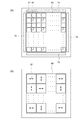
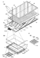
【解決手段】第1の基板、第2の基板、第1の素子層、および第2の素子層を有する表示装置であって、第1の素子層は、第1の基板と第2の基板との間に設けられ、第2の素子層は、第1の基板と第2の基板との間に設けられ、第1の素子層と第2の素子層とは、互いに重なる領域を有し、第1の基板および第2の基板は可撓性を有し、第1の素子層は、表示素子および第1の回路を有し、表示素子は、第1の回路と電気的に接続され、第2の素子層はセンサ素子を有し、センサ素子は、歪を検出することができる機能を有する構成の表示装置とする。
【選択図】図1
Description
本実施の形態では、本発明の一態様の表示装置について図面を用いて説明する。
本実施の形態では、本発明の一態様の表示装置を用いて、実施の形態1の図7(A)、(B)に示す表示を行うための方法の一例について説明する。
本実施の形態では、実施の形態1で説明した歪センサ素子および歪センサ素子の抵抗変化量を読み出す機能を有する第2の回路について説明する。なお、本実施の形態では歪センサ素子と電気的に接続された第2の回路を歪センサ回路と称する。

本実施の形態では、本発明の一態様の表示装置に用いることのできるトランジスタおよび該トランジスタを構成する材料について説明する。本実施の形態で説明するトランジスタは、先の実施の形態で説明したトランジスタ350、352、354、501、502、503、504、505などに用いることができる。
以下では、本発明の一態様に用いることのできる酸化物半導体膜の構造について説明する。
本実施の形態では、本発明の一態様の表示装置を用いることができる表示モジュールについて説明を行う。
本実施の形態では、本発明の一態様の歪センサ素子を備える表示装置を用いることのできるタッチパネルについて説明する。
図26は本発明の一態様のタッチパネルの構成を説明する投影図および斜視図である。図26(A)は本発明の一態様のタッチパネル700、およびタッチパネル700が備える検知ユニット800の構成を説明する投影図である。
検知素子Cについて、容量素子を用いた一例を挙げて説明する。当該容量素子は、一対の電極を有する。一対の電極間には、誘電体層として絶縁膜を有する。
図27は本発明の一態様の検知回路19、変換器CONVの構成および駆動方法を説明する図である。
検知回路19の駆動方法について説明する。
第1のステップにおいて、トランジスタM3を導通状態にした後に非導通状態にするリセット信号をゲートに供給し、検知素子Cの第1の電極の電位を所定の電位にする(図27(B−1)期間T1参照)。
第2のステップにおいて、トランジスタM2を導通状態にする選択信号をゲートに供給し、トランジスタM1の第2の電極を信号線DLに電気的に接続する。
第3のステップにおいて、制御信号を検知素子の第2の電極に供給し、制御信号および検知素子Cの容量に基づいて変化する電位をトランジスタM1のゲートに供給する。
第4のステップにおいて、トランジスタM1のゲートの電位の変化がもたらす信号を信号線DLに供給する。
第5のステップにおいて、トランジスタM2を非導通状態にする選択信号をゲートに供給する。
本実施の形態では、本発明の一態様の表示装置を用いて構成することができる情報処理装置の構成について、図30を参照しながら説明する。
本実施の形態で説明する情報処理装置6000は、画像情報Vを供給され、検知情報Sを供給する入出力装置6020と、画像情報Vを供給し、検知情報Sを供給される演算装置6010と、を有する。
本実施の形態では、本発明の一態様が適用された電子機器について、図31を用いて説明する。
16 基材
17 保護基材
17p 保護層
19 検知回路
41 基板
42 基板
50 素子層
51 素子層
52 素子層
71 回路
72 回路
73 回路
74 回路
80 画素部
81 画素
82 歪センサ素子
91 歪センサ回路部
92 画素回路部
92a 画素回路部
92d 画素回路部
100 入力装置
300 表示装置
302 領域
303 領域
304 領域
305 領域
306 領域
312 シール材
316 FPC
321a 絶縁膜
321b 絶縁膜
334 絶縁膜
336 着色層
338 遮光層
340 容量素子
341 電極
342 電極
350 トランジスタ
352 トランジスタ
354 トランジスタ
354a トランジスタ
354b トランジスタ
360 接続電極
364 絶縁膜
366 絶縁層
368 絶縁膜
370 平坦化絶縁膜
371 平坦化絶縁膜
372 導電膜
374 導電膜
380 異方性導電膜
430 絶縁膜
432 封止層
446 EL層
480 有機EL素子
501 トランジスタ
502 トランジスタ
503 トランジスタ
504 トランジスタ
505 トランジスタ
510 可変抵抗素子
520 抵抗素子
530 配線
540 配線
545 配線
550 配線
560 配線
570 配線
580 配線
590 配線
610 容量素子
620 有機EL素子
625 液晶素子
630 セレクタ
640 トランジスタ
650 トランジスタ
660 アンプ
670 アナログ−デジタル変換器
700 タッチパネル
701 表示部
702 画素
702B 副画素
702G 副画素
702R 副画素
703g 走査線駆動回路
710 基材
711 配線
719 端子
767p 反射防止層
800 検知ユニット
900 基板
915 絶縁膜
920 ゲート電極層
921 導電膜
930 ゲート絶縁膜
931 絶縁膜
932 絶縁膜
933 絶縁膜
940 酸化物半導体層
941a 酸化物半導体層
941b 酸化物半導体層
942a 酸化物半導体層
942b 酸化物半導体層
942c 酸化物半導体層
950 ソース電極層
951 ソース領域
960 ドレイン電極層
961 ドレイン領域
970 絶縁膜
975 絶縁膜
980 絶縁膜
990 絶縁膜
5000 表示装置
5001 表示部
5002 歪センサ部
5010 回路
5020 回路
5030 回路
5040 映像信号出力装置
5050 回路
5060 制御装置
6000 情報処理装置
6001 筐体
6002 ヒンジ
6010 演算装置
6010A アンテナ
6010B バッテリー
6020 入出力装置
6030 表示部
6031 領域
6045 ボタン
7100 携帯型情報端末
7101 筐体
7102 表示部
7105 スピーカ
7106 マイク
7107 カメラ
7200 大型ディスプレイ
7201 筐体
7202 表示部
7203 センサ
7300 腕章
7301 筒状体
7302 表示部
7400 衣服
7401 布地
7402 表示部
8000 表示モジュール
8001 上部カバー
8002 下部カバー
8003 FPC
8004 タッチパネル
8005 FPC
8006 表示パネル
8007 バックライト
8008 光源
8009 フレーム
8010 プリント基板
8011 バッテリー
Claims (14)
- 第1の基板、第2の基板、第1の素子層、および第2の素子層を有する表示装置であって、
前記第1の素子層は、前記第1の基板と前記第2の基板との間に設けられ、
前記第2の素子層は、前記第1の基板と前記第2の基板との間に設けられ、
前記第1の素子層と前記第2の素子層とは、互いに重なる領域を有し、
前記第1の基板および前記第2の基板は可撓性を有し、
前記第1の素子層は、表示素子および第1の回路を有し、
前記表示素子は、前記第1の回路と電気的に接続され、
前記第2の素子層はセンサ素子を有し、
前記センサ素子は、前記第1の基板または前記第2の基板の歪を検出することができる機能を有することを特徴とする表示装置。 - 請求項1において、
前記第2の素子層は第2の回路を有し、
前記第2の回路は、前記センサ素子と電気的に接続されていることを特徴とする表示装置。 - 第1の基板、第2の基板、および素子層を有する表示装置であって、
前記素子層は、前記第1の基板と前記第2の基板との間に設けられ、
前記第1の基板および前記第2の基板は可撓性を有し、
前記素子層は、表示素子、センサ素子、第1の回路および第2の回路を有し、
前記表示素子は、前記第1の回路と電気的に接続され、
前記センサ素子は、前記第2の回路と電気的に接続され、
前記センサ素子は、前記第1の基板または前記第2の基板の歪を検出することができる機能を有することを特徴とする表示装置。 - 請求項2または3において、
前記第1の回路および前記第2の回路は、チャネル形成領域が酸化物半導体で設けられたトランジスタを有することを特徴とする表示装置。 - 請求項4において、
前記酸化物半導体は、InとZnと、M(MはAl、Ti、Ga、Sn、Y、Zr、La、Ce、NdまたはHf)とを有することを特徴とする表示装置。 - 請求項4または5において、
前記酸化物半導体はc軸に配向する結晶を有することを特徴とする表示装置。 - 請求項1乃至6のいずれか一項において、
前記センサ素子は、金属薄膜抵抗素子であることを特徴とする表示装置。 - 請求項1乃至7のいずれか一項において、
前記表示素子は、有機EL素子であることを特徴とする表示装置。 - 画像情報を取り込み、仮想画面を構成する第1のステップと、
表示部の形状情報を取り込み、3次元形状モデルを構成する第2のステップと、
視認者の位置情報を取り込み、前記3次元形状モデルから二次元の表示部を想定し、当該表示部に座標を割り当てる第3のステップと、
前記表示部の、視認者の位置から見えない部分を算出する第4のステップと、
仮想画面の座標を前記二次元の表示部の座標に変換する第5のステップと、
前記第5のステップで得られた画像情報を前記表示部に出力する第6のステップと、
を有することを特徴とする表示装置の動作方法。 - 画像情報を取り込み、仮想画面を構成する第1のステップと、
表示装置および視認者の状況を検出する第2のステップと、
表示部の形状情報を取り込み、3次元形状モデルを構成する第3のステップと、
視認者の位置情報を取り込み、前記3次元形状モデルから二次元の表示部を想定し、当該表示部に座標を割り当てる第4のステップと、
前記表示部の、視認者の位置から見えない部分を算出する第5のステップと、
前記仮想画面の座標を前記二次元の表示部の座標に変換する第6のステップと、
前記第6のステップで得られた画像情報を前記表示部に出力する第7のステップと、
を有し、
前記第2のステップ乃至前記第7のステップを順に実行することを特徴とする表示装置の動作方法。 - 請求項10において、
前記第2のステップは、
表示部の形状が変化したか否かを判断する第8のステップと、
視認者の位置が変化したか否かを判断する第9のステップと、
画像変更命令が出たか否かを判断する第10のステップと、
を有し、
前記第8のステップにおいて、
前記表示部の形状が変化した場合は、前記第3のステップに進み、
前記表示部の形状が変化していない場合は、前記第9のステップに進み、
前記第9のステップにおいて、
前記視認者の位置が変化した場合は、前記第4のステップに進み、
前記視認者の位置が変化していない場合は、前記第10のステップに進み、
前記第10のステップにおいて、
前記画像変更命令が出た場合は、前記第1のステップに進み、
前記第1のステップの実行後に前記第6のステップに進み、
前記画像変更命令が出ていない場合は、前記第2のステップに戻ることを特徴とする表示装置の動作方法。 - 請求項10または11において、
前記第7のステップから前記第2のステップに戻る動作を有することを特徴とする表示装置の動作方法。 - 請求項1乃至8のいずれか一項に記載の表示装置と、
FPC、または、フレームと、
を有する表示モジュール。 - 請求項1乃至8のいずれか一項に記載の表示装置、または、請求項9に記載の表示モジュールと、
スピーカ、マイク、または、カメラと、
を有する電子機器。
Priority Applications (1)
| Application Number | Priority Date | Filing Date | Title |
|---|---|---|---|
| JP2015084176A JP6721294B2 (ja) | 2014-04-18 | 2015-04-16 | 表示装置 |
Applications Claiming Priority (5)
| Application Number | Priority Date | Filing Date | Title |
|---|---|---|---|
| JP2014086089 | 2014-04-18 | ||
| JP2014086089 | 2014-04-18 | ||
| JP2014095331 | 2014-05-02 | ||
| JP2014095331 | 2014-05-02 | ||
| JP2015084176A JP6721294B2 (ja) | 2014-04-18 | 2015-04-16 | 表示装置 |
Related Child Applications (1)
| Application Number | Title | Priority Date | Filing Date |
|---|---|---|---|
| JP2020105205A Division JP2020160477A (ja) | 2014-04-18 | 2020-06-18 | 表示装置の動作方法 |
Publications (3)
| Publication Number | Publication Date |
|---|---|
| JP2015228014A true JP2015228014A (ja) | 2015-12-17 |
| JP2015228014A5 JP2015228014A5 (ja) | 2018-05-17 |
| JP6721294B2 JP6721294B2 (ja) | 2020-07-15 |
Family
ID=54322028
Family Applications (2)
| Application Number | Title | Priority Date | Filing Date |
|---|---|---|---|
| JP2015084176A Active JP6721294B2 (ja) | 2014-04-18 | 2015-04-16 | 表示装置 |
| JP2020105205A Withdrawn JP2020160477A (ja) | 2014-04-18 | 2020-06-18 | 表示装置の動作方法 |
Family Applications After (1)
| Application Number | Title | Priority Date | Filing Date |
|---|---|---|---|
| JP2020105205A Withdrawn JP2020160477A (ja) | 2014-04-18 | 2020-06-18 | 表示装置の動作方法 |
Country Status (4)
| Country | Link |
|---|---|
| US (2) | US9952724B2 (ja) |
| JP (2) | JP6721294B2 (ja) |
| KR (1) | KR102511325B1 (ja) |
| TW (2) | TWI673692B (ja) |
Cited By (9)
| Publication number | Priority date | Publication date | Assignee | Title |
|---|---|---|---|---|
| JP2017142340A (ja) * | 2016-02-09 | 2017-08-17 | レノボ・シンガポール・プライベート・リミテッド | 情報処理装置、画像表示制御方法、及びプログラム |
| JP2018010293A (ja) * | 2016-06-30 | 2018-01-18 | 株式会社半導体エネルギー研究所 | 情報端末 |
| JP2018072451A (ja) * | 2016-10-26 | 2018-05-10 | 株式会社ジャパンディスプレイ | 表示装置、および表示装置の作製方法 |
| JP2018085110A (ja) * | 2016-11-17 | 2018-05-31 | 株式会社半導体エネルギー研究所 | 電子機器、及びタッチパネル入力方法 |
| WO2018163348A1 (ja) * | 2017-03-09 | 2018-09-13 | Necディスプレイソリューションズ株式会社 | 映像表示装置、映像表示装置の制御方法 |
| JP2019536255A (ja) * | 2016-11-30 | 2019-12-12 | 京東方科技集團股▲ふん▼有限公司Boe Technology Group Co.,Ltd. | 薄膜トランジスタの製造方法、薄膜トランジスタ及び表示装置 |
| JP2020532091A (ja) * | 2017-08-23 | 2020-11-05 | 京東方科技集團股▲ふん▼有限公司Boe Technology Group Co.,Ltd. | 可撓性基板およびその製造方法、屈曲検出方法ならびに可撓性表示装置 |
| JP2021117275A (ja) * | 2020-01-23 | 2021-08-10 | セイコーエプソン株式会社 | 電気光学装置および電子機器 |
| JP2022105300A (ja) * | 2020-12-31 | 2022-07-13 | エルジー ディスプレイ カンパニー リミテッド | 表示装置 |
Families Citing this family (42)
| Publication number | Priority date | Publication date | Assignee | Title |
|---|---|---|---|---|
| US10656799B2 (en) | 2014-05-02 | 2020-05-19 | Semiconductor Energy Laboratory Co., Ltd. | Display device and operation method thereof |
| KR102338003B1 (ko) * | 2014-10-07 | 2021-12-10 | 삼성전자 주식회사 | 플렉서블 디스플레이를 포함하는 전자 장치 |
| KR102919714B1 (ko) | 2014-11-28 | 2026-01-28 | 가부시키가이샤 한도오따이 에네루기 켄큐쇼 | 표시 장치, 모듈, 표시 시스템, 및 전자 기기 |
| KR102362196B1 (ko) * | 2015-02-02 | 2022-02-11 | 삼성디스플레이 주식회사 | 유기 발광 표시 장치 및 그 제조 방법 |
| JP6441168B2 (ja) * | 2015-05-29 | 2018-12-19 | 株式会社ジャパンディスプレイ | センサ付き表示装置 |
| US10133428B2 (en) * | 2015-05-29 | 2018-11-20 | Samsung Display Co., Ltd. | Flexible display device including a flexible substrate having a bending part and a conductive pattern at least partially disposed on the bending part |
| CN104933989B (zh) * | 2015-06-26 | 2017-04-26 | 京东方科技集团股份有限公司 | 检测电路、像素电信号采集电路、显示面板和显示装置 |
| US10725207B2 (en) * | 2015-08-19 | 2020-07-28 | Young Optics Inc. | Optical apparatus having organic-inorganic composite material |
| US10485100B2 (en) | 2015-09-30 | 2019-11-19 | Semiconductor Energy Laboratory Co., Ltd. | Circuit board and display system |
| CN108352149B (zh) * | 2015-12-02 | 2020-11-03 | 夏普株式会社 | 挠性显示装置及其弯曲状态检测方法 |
| KR20170070574A (ko) * | 2015-12-14 | 2017-06-22 | 삼성전자주식회사 | 플렉서블 디스플레이를 가지는 전자 장치 및 그의 제어 방법 |
| US10572083B2 (en) * | 2015-12-25 | 2020-02-25 | Shenzhen Royole Technologies Co., Ltd. | Flexible display screen system |
| CN106293449B (zh) * | 2016-02-04 | 2020-03-03 | 北京智谷睿拓技术服务有限公司 | 交互方法、交互装置及用户设备 |
| CN106250074B (zh) * | 2016-02-04 | 2019-09-10 | 北京智谷睿拓技术服务有限公司 | 交互方法、交互装置及用户设备 |
| CN106325588B (zh) * | 2016-02-04 | 2019-11-15 | 北京智谷睿拓技术服务有限公司 | 交互方法、交互装置及用户设备 |
| CN106325718B (zh) * | 2016-02-04 | 2019-11-29 | 北京智谷睿拓技术服务有限公司 | 交互方法、交互装置及用户设备 |
| CN106249861B (zh) * | 2016-02-04 | 2019-09-27 | 北京智谷睿拓技术服务有限公司 | 交互方法、交互装置及用户设备 |
| CN106249863B (zh) * | 2016-02-04 | 2019-02-12 | 北京智谷睿拓技术服务有限公司 | 交互方法、交互装置及用户设备 |
| CN106249862B (zh) * | 2016-02-04 | 2019-02-15 | 北京智谷睿拓技术服务有限公司 | 交互方法、交互装置及用户设备 |
| US10911742B2 (en) * | 2016-03-08 | 2021-02-02 | Motorola Mobility Llc | Electronic device with flexible display and louvered filter, and corresponding systems and methods |
| KR102518427B1 (ko) * | 2016-03-14 | 2023-04-05 | 삼성디스플레이 주식회사 | 표시 장치 |
| KR102475589B1 (ko) * | 2016-04-29 | 2022-12-07 | 엘지디스플레이 주식회사 | 플렉서블 유기발광 표시장치 |
| KR102482398B1 (ko) * | 2016-04-29 | 2022-12-27 | 엘지디스플레이 주식회사 | 터치 스크린 장치 및 이를 포함하는 전자 기기 |
| JP6998690B2 (ja) * | 2016-07-28 | 2022-01-18 | 株式会社半導体エネルギー研究所 | 情報端末 |
| US10620689B2 (en) * | 2016-10-21 | 2020-04-14 | Semiconductor Energy Laboratory Co., Ltd. | Display device, electronic device, and operation method thereof |
| KR102592857B1 (ko) * | 2016-12-16 | 2023-10-24 | 삼성디스플레이 주식회사 | 표시패널 및 이를 포함하는 표시장치 |
| DE102017200949B4 (de) * | 2017-01-20 | 2019-05-02 | Audi Ag | Kombiinstrument mit verformbarer Anzeige und Fahrzeug mit einem Kombiinstrument |
| US10777758B2 (en) * | 2017-01-27 | 2020-09-15 | Sharp Kabushiki Kaisha | Display device |
| EP3588480B1 (en) | 2017-02-22 | 2021-09-01 | Kunshan Go-Visionox Opto-Electronics Co., Ltd. | Pixel driving circuit and driving method thereof, and layout structure of transistor |
| KR101910518B1 (ko) * | 2017-04-11 | 2018-10-22 | 삼성전자주식회사 | 생체 센서 및 생체 센서를 포함하는 장치 |
| WO2019003037A1 (ja) | 2017-06-27 | 2019-01-03 | 株式会社半導体エネルギー研究所 | 半導体装置および電子部品 |
| EP3712946A1 (en) * | 2017-11-17 | 2020-09-23 | Shenzhen Royole Technologies Co., Ltd. | Organic light emitting diode display module and manufacturing method therefor, and electronic device |
| KR102502201B1 (ko) | 2017-11-17 | 2023-02-22 | 삼성디스플레이 주식회사 | 지문 센서 및 이를 포함한 표시 장치 |
| CN110164340B (zh) | 2018-12-06 | 2021-01-26 | 京东方科技集团股份有限公司 | 补偿装置、显示屏、显示装置和补偿方法 |
| KR20210116475A (ko) | 2019-01-18 | 2021-09-27 | 가부시키가이샤 한도오따이 에네루기 켄큐쇼 | 표시 시스템, 표시 장치, 발광 장치 |
| CN109814304B (zh) * | 2019-03-18 | 2023-01-17 | 京东方科技集团股份有限公司 | 显示面板和显示装置 |
| KR102723141B1 (ko) * | 2019-12-02 | 2024-10-30 | 삼성디스플레이 주식회사 | 플렉서블 표시 장치, 및 플렉서블 표시 장치의 구동 방법 |
| CN112951166B (zh) * | 2021-03-31 | 2022-10-04 | 合肥维信诺科技有限公司 | 驱动ic、显示面板的驱动方法、显示面板及显示装置 |
| TWI794909B (zh) * | 2021-07-29 | 2023-03-01 | 日商雅馬哈智能機器控股股份有限公司 | 三維畫像產生裝置以及三維畫像產生方法 |
| KR20230109211A (ko) * | 2022-01-12 | 2023-07-20 | 삼성디스플레이 주식회사 | 표시패널 |
| US11989065B2 (en) * | 2022-01-18 | 2024-05-21 | Stmicroelectronics S.R.L. | Screen state detection using an electrostatic charge variation sensor |
| KR20230136362A (ko) * | 2022-03-18 | 2023-09-26 | 매그나칩 반도체 유한회사 | 디스플레이 패널의 소스 드라이버 |
Citations (14)
| Publication number | Priority date | Publication date | Assignee | Title |
|---|---|---|---|---|
| JPH09258893A (ja) * | 1996-03-25 | 1997-10-03 | Toshiba Corp | 座標入力装置、およびこれを備えた入力表示装置 |
| JP2007048237A (ja) * | 2005-08-12 | 2007-02-22 | Ricoh Co Ltd | 表示装置、制御装置、情報処理装置及び表示制御方法、表示制御プログラム |
| JP2010157060A (ja) * | 2008-12-26 | 2010-07-15 | Sony Corp | 表示装置 |
| JP2011119179A (ja) * | 2009-12-07 | 2011-06-16 | Fujifilm Corp | 電子デバイスの製造方法、放射線センサの製造方法及び有機el表示装置の製造方法 |
| JP2012128227A (ja) * | 2010-12-16 | 2012-07-05 | Seiko Epson Corp | 情報表示端末 |
| US20120256720A1 (en) * | 2011-04-08 | 2012-10-11 | Samsung Electronics Co., Ltd. | Bending sensor and method for fabricating the same |
| JP2013503388A (ja) * | 2009-08-26 | 2013-01-31 | グローバル・オーエルイーディー・テクノロジー・リミテッド・ライアビリティ・カンパニー | フレキシブルマルチタッチセンシングエレクトロルミネッセントディスプレイ |
| WO2013048925A2 (en) * | 2011-09-30 | 2013-04-04 | Apple Inc. | Flexible electronic devices |
| JP2013127366A (ja) * | 2010-03-29 | 2013-06-27 | Sharp Corp | 圧力検出装置およびその製造方法、表示装置およびその製造方法、ならびに圧力検出装置付きtft基板 |
| JP2013242437A (ja) * | 2012-05-21 | 2013-12-05 | Panasonic Corp | 画像表示装置 |
| JP2013254021A (ja) * | 2012-06-05 | 2013-12-19 | Sony Corp | 表示装置および電子機器 |
| WO2013190813A1 (ja) * | 2012-06-21 | 2013-12-27 | パナソニック株式会社 | 有機el表示装置およびその製造方法 |
| JP2014006523A (ja) * | 2012-06-22 | 2014-01-16 | Samsung Display Co Ltd | フレキシブル表示装置 |
| JP2014029690A (ja) * | 2012-07-30 | 2014-02-13 | Samsung Electronics Co Ltd | ベンディングインタラクションガイドを提供するフレキシブル装置及びその制御方法 |
Family Cites Families (131)
| Publication number | Priority date | Publication date | Assignee | Title |
|---|---|---|---|---|
| JPS60198861A (ja) | 1984-03-23 | 1985-10-08 | Fujitsu Ltd | 薄膜トランジスタ |
| JPH0244256B2 (ja) | 1987-01-28 | 1990-10-03 | Kagaku Gijutsucho Mukizaishitsu Kenkyushocho | Ingazn2o5deshimesarerurotsuhoshokeinosojokozoojusurukagobutsuoyobisonoseizoho |
| JPH0244258B2 (ja) | 1987-02-24 | 1990-10-03 | Kagaku Gijutsucho Mukizaishitsu Kenkyushocho | Ingazn3o6deshimesarerurotsuhoshokeinosojokozoojusurukagobutsuoyobisonoseizoho |
| JPH0244260B2 (ja) | 1987-02-24 | 1990-10-03 | Kagaku Gijutsucho Mukizaishitsu Kenkyushocho | Ingazn5o8deshimesarerurotsuhoshokeinosojokozoojusurukagobutsuoyobisonoseizoho |
| JPS63210023A (ja) | 1987-02-24 | 1988-08-31 | Natl Inst For Res In Inorg Mater | InGaZn↓4O↓7で示される六方晶系の層状構造を有する化合物およびその製造法 |
| JPH0244262B2 (ja) | 1987-02-27 | 1990-10-03 | Kagaku Gijutsucho Mukizaishitsu Kenkyushocho | Ingazn6o9deshimesarerurotsuhoshokeinosojokozoojusurukagobutsuoyobisonoseizoho |
| JPH0244263B2 (ja) | 1987-04-22 | 1990-10-03 | Kagaku Gijutsucho Mukizaishitsu Kenkyushocho | Ingazn7o10deshimesarerurotsuhoshokeinosojokozoojusurukagobutsuoyobisonoseizoho |
| JPH05251705A (ja) | 1992-03-04 | 1993-09-28 | Fuji Xerox Co Ltd | 薄膜トランジスタ |
| JP3479375B2 (ja) | 1995-03-27 | 2003-12-15 | 科学技術振興事業団 | 亜酸化銅等の金属酸化物半導体による薄膜トランジスタとpn接合を形成した金属酸化物半導体装置およびそれらの製造方法 |
| WO1997006554A2 (en) | 1995-08-03 | 1997-02-20 | Philips Electronics N.V. | Semiconductor device provided with transparent switching element |
| JP3625598B2 (ja) | 1995-12-30 | 2005-03-02 | 三星電子株式会社 | 液晶表示装置の製造方法 |
| JP4170454B2 (ja) | 1998-07-24 | 2008-10-22 | Hoya株式会社 | 透明導電性酸化物薄膜を有する物品及びその製造方法 |
| JP2000150861A (ja) | 1998-11-16 | 2000-05-30 | Tdk Corp | 酸化物薄膜 |
| JP3276930B2 (ja) | 1998-11-17 | 2002-04-22 | 科学技術振興事業団 | トランジスタ及び半導体装置 |
| TW460731B (en) | 1999-09-03 | 2001-10-21 | Ind Tech Res Inst | Electrode structure and production method of wide viewing angle LCD |
| JP4089858B2 (ja) | 2000-09-01 | 2008-05-28 | 国立大学法人東北大学 | 半導体デバイス |
| KR20020038482A (ko) | 2000-11-15 | 2002-05-23 | 모리시타 요이찌 | 박막 트랜지스터 어레이, 그 제조방법 및 그것을 이용한표시패널 |
| JP4560974B2 (ja) | 2001-03-15 | 2010-10-13 | コニカミノルタビジネステクノロジーズ株式会社 | 画像表示装置 |
| JP3997731B2 (ja) | 2001-03-19 | 2007-10-24 | 富士ゼロックス株式会社 | 基材上に結晶性半導体薄膜を形成する方法 |
| JP2002289859A (ja) | 2001-03-23 | 2002-10-04 | Minolta Co Ltd | 薄膜トランジスタ |
| US8415208B2 (en) | 2001-07-16 | 2013-04-09 | Semiconductor Energy Laboratory Co., Ltd. | Semiconductor device and peeling off method and method of manufacturing semiconductor device |
| JP4027740B2 (ja) | 2001-07-16 | 2007-12-26 | 株式会社半導体エネルギー研究所 | 半導体装置の作製方法 |
| JP4090716B2 (ja) | 2001-09-10 | 2008-05-28 | 雅司 川崎 | 薄膜トランジスタおよびマトリクス表示装置 |
| JP3925839B2 (ja) | 2001-09-10 | 2007-06-06 | シャープ株式会社 | 半導体記憶装置およびその試験方法 |
| EP1443130B1 (en) | 2001-11-05 | 2011-09-28 | Japan Science and Technology Agency | Natural superlattice homologous single crystal thin film, method for preparation thereof, and device using said single crystal thin film |
| JP4164562B2 (ja) | 2002-09-11 | 2008-10-15 | 独立行政法人科学技術振興機構 | ホモロガス薄膜を活性層として用いる透明薄膜電界効果型トランジスタ |
| JP4083486B2 (ja) | 2002-02-21 | 2008-04-30 | 独立行政法人科学技術振興機構 | LnCuO(S,Se,Te)単結晶薄膜の製造方法 |
| CN1445821A (zh) | 2002-03-15 | 2003-10-01 | 三洋电机株式会社 | ZnO膜和ZnO半导体层的形成方法、半导体元件及其制造方法 |
| JP3933591B2 (ja) | 2002-03-26 | 2007-06-20 | 淳二 城戸 | 有機エレクトロルミネッセント素子 |
| US7339187B2 (en) | 2002-05-21 | 2008-03-04 | State Of Oregon Acting By And Through The Oregon State Board Of Higher Education On Behalf Of Oregon State University | Transistor structures |
| JP2004022625A (ja) | 2002-06-13 | 2004-01-22 | Murata Mfg Co Ltd | 半導体デバイス及び該半導体デバイスの製造方法 |
| US7105868B2 (en) | 2002-06-24 | 2006-09-12 | Cermet, Inc. | High-electron mobility transistor with zinc oxide |
| TW564373B (en) * | 2002-09-19 | 2003-12-01 | Via Tech Inc | Partial image rotation device and method |
| US7067843B2 (en) | 2002-10-11 | 2006-06-27 | E. I. Du Pont De Nemours And Company | Transparent oxide semiconductor thin film transistors |
| JP4166105B2 (ja) | 2003-03-06 | 2008-10-15 | シャープ株式会社 | 半導体装置およびその製造方法 |
| JP2004273732A (ja) | 2003-03-07 | 2004-09-30 | Sharp Corp | アクティブマトリクス基板およびその製造方法 |
| JP4108633B2 (ja) | 2003-06-20 | 2008-06-25 | シャープ株式会社 | 薄膜トランジスタおよびその製造方法ならびに電子デバイス |
| US7262463B2 (en) | 2003-07-25 | 2007-08-28 | Hewlett-Packard Development Company, L.P. | Transistor including a deposited channel region having a doped portion |
| US7297977B2 (en) | 2004-03-12 | 2007-11-20 | Hewlett-Packard Development Company, L.P. | Semiconductor device |
| US7282782B2 (en) | 2004-03-12 | 2007-10-16 | Hewlett-Packard Development Company, L.P. | Combined binary oxide semiconductor device |
| US7145174B2 (en) | 2004-03-12 | 2006-12-05 | Hewlett-Packard Development Company, Lp. | Semiconductor device |
| EP2413366B1 (en) | 2004-03-12 | 2017-01-11 | Japan Science And Technology Agency | A switching element of LCDs or organic EL displays |
| US7211825B2 (en) | 2004-06-14 | 2007-05-01 | Yi-Chi Shih | Indium oxide-based thin film transistors and circuits |
| JP2006100760A (ja) | 2004-09-02 | 2006-04-13 | Casio Comput Co Ltd | 薄膜トランジスタおよびその製造方法 |
| US7285501B2 (en) | 2004-09-17 | 2007-10-23 | Hewlett-Packard Development Company, L.P. | Method of forming a solution processed device |
| US7298084B2 (en) | 2004-11-02 | 2007-11-20 | 3M Innovative Properties Company | Methods and displays utilizing integrated zinc oxide row and column drivers in conjunction with organic light emitting diodes |
| RU2369940C2 (ru) | 2004-11-10 | 2009-10-10 | Кэнон Кабусики Кайся | Аморфный оксид и полевой транзистор с его использованием |
| US7829444B2 (en) | 2004-11-10 | 2010-11-09 | Canon Kabushiki Kaisha | Field effect transistor manufacturing method |
| US7863611B2 (en) | 2004-11-10 | 2011-01-04 | Canon Kabushiki Kaisha | Integrated circuits utilizing amorphous oxides |
| US7791072B2 (en) | 2004-11-10 | 2010-09-07 | Canon Kabushiki Kaisha | Display |
| CA2585063C (en) | 2004-11-10 | 2013-01-15 | Canon Kabushiki Kaisha | Light-emitting device |
| US7453065B2 (en) | 2004-11-10 | 2008-11-18 | Canon Kabushiki Kaisha | Sensor and image pickup device |
| JP5126729B2 (ja) | 2004-11-10 | 2013-01-23 | キヤノン株式会社 | 画像表示装置 |
| EP1815530B1 (en) | 2004-11-10 | 2021-02-17 | Canon Kabushiki Kaisha | Field effect transistor employing an amorphous oxide |
| JP4687102B2 (ja) * | 2004-12-27 | 2011-05-25 | 凸版印刷株式会社 | 画像表示装置及び画像表示システム |
| US7579224B2 (en) | 2005-01-21 | 2009-08-25 | Semiconductor Energy Laboratory Co., Ltd. | Method for manufacturing a thin film semiconductor device |
| TWI390735B (zh) | 2005-01-28 | 2013-03-21 | 半導體能源研究所股份有限公司 | 半導體裝置,電子裝置,和半導體裝置的製造方法 |
| TWI505473B (zh) | 2005-01-28 | 2015-10-21 | 半導體能源研究所股份有限公司 | 半導體裝置,電子裝置,和半導體裝置的製造方法 |
| US7858451B2 (en) | 2005-02-03 | 2010-12-28 | Semiconductor Energy Laboratory Co., Ltd. | Electronic device, semiconductor device and manufacturing method thereof |
| US7948171B2 (en) | 2005-02-18 | 2011-05-24 | Semiconductor Energy Laboratory Co., Ltd. | Light emitting device |
| US20060197092A1 (en) | 2005-03-03 | 2006-09-07 | Randy Hoffman | System and method for forming conductive material on a substrate |
| JP2006243621A (ja) * | 2005-03-07 | 2006-09-14 | Canon Inc | 表示装置 |
| US8681077B2 (en) | 2005-03-18 | 2014-03-25 | Semiconductor Energy Laboratory Co., Ltd. | Semiconductor device, and display device, driving method and electronic apparatus thereof |
| WO2006105077A2 (en) | 2005-03-28 | 2006-10-05 | Massachusetts Institute Of Technology | Low voltage thin film transistor with high-k dielectric material |
| US7645478B2 (en) | 2005-03-31 | 2010-01-12 | 3M Innovative Properties Company | Methods of making displays |
| US8300031B2 (en) | 2005-04-20 | 2012-10-30 | Semiconductor Energy Laboratory Co., Ltd. | Semiconductor device comprising transistor having gate and drain connected through a current-voltage conversion element |
| JP2006344849A (ja) | 2005-06-10 | 2006-12-21 | Casio Comput Co Ltd | 薄膜トランジスタ |
| US7402506B2 (en) | 2005-06-16 | 2008-07-22 | Eastman Kodak Company | Methods of making thin film transistors comprising zinc-oxide-based semiconductor materials and transistors made thereby |
| US7691666B2 (en) | 2005-06-16 | 2010-04-06 | Eastman Kodak Company | Methods of making thin film transistors comprising zinc-oxide-based semiconductor materials and transistors made thereby |
| US7507618B2 (en) | 2005-06-27 | 2009-03-24 | 3M Innovative Properties Company | Method for making electronic devices using metal oxide nanoparticles |
| KR100711890B1 (ko) | 2005-07-28 | 2007-04-25 | 삼성에스디아이 주식회사 | 유기 발광표시장치 및 그의 제조방법 |
| JP2007059128A (ja) | 2005-08-23 | 2007-03-08 | Canon Inc | 有機el表示装置およびその製造方法 |
| JP5116225B2 (ja) | 2005-09-06 | 2013-01-09 | キヤノン株式会社 | 酸化物半導体デバイスの製造方法 |
| JP4280736B2 (ja) | 2005-09-06 | 2009-06-17 | キヤノン株式会社 | 半導体素子 |
| JP2007073705A (ja) | 2005-09-06 | 2007-03-22 | Canon Inc | 酸化物半導体チャネル薄膜トランジスタおよびその製造方法 |
| JP4850457B2 (ja) | 2005-09-06 | 2012-01-11 | キヤノン株式会社 | 薄膜トランジスタ及び薄膜ダイオード |
| EP3614442A3 (en) | 2005-09-29 | 2020-03-25 | Semiconductor Energy Laboratory Co., Ltd. | Semiconductor device having oxide semiconductor layer and manufactoring method thereof |
| JP5037808B2 (ja) | 2005-10-20 | 2012-10-03 | キヤノン株式会社 | アモルファス酸化物を用いた電界効果型トランジスタ、及び該トランジスタを用いた表示装置 |
| CN101283444B (zh) | 2005-11-15 | 2011-01-26 | 株式会社半导体能源研究所 | 半导体器件及其制造方法 |
| TWI292281B (en) | 2005-12-29 | 2008-01-01 | Ind Tech Res Inst | Pixel structure of active organic light emitting diode and method of fabricating the same |
| US7867636B2 (en) | 2006-01-11 | 2011-01-11 | Murata Manufacturing Co., Ltd. | Transparent conductive film and method for manufacturing the same |
| JP4977478B2 (ja) | 2006-01-21 | 2012-07-18 | 三星電子株式会社 | ZnOフィルム及びこれを用いたTFTの製造方法 |
| US7576394B2 (en) | 2006-02-02 | 2009-08-18 | Kochi Industrial Promotion Center | Thin film transistor including low resistance conductive thin films and manufacturing method thereof |
| US7977169B2 (en) | 2006-02-15 | 2011-07-12 | Kochi Industrial Promotion Center | Semiconductor device including active layer made of zinc oxide with controlled orientations and manufacturing method thereof |
| KR20070101595A (ko) | 2006-04-11 | 2007-10-17 | 삼성전자주식회사 | ZnO TFT |
| US20070252928A1 (en) | 2006-04-28 | 2007-11-01 | Toppan Printing Co., Ltd. | Structure, transmission type liquid crystal display, reflection type display and manufacturing method thereof |
| JP5028033B2 (ja) | 2006-06-13 | 2012-09-19 | キヤノン株式会社 | 酸化物半導体膜のドライエッチング方法 |
| JP4999400B2 (ja) | 2006-08-09 | 2012-08-15 | キヤノン株式会社 | 酸化物半導体膜のドライエッチング方法 |
| JP4609797B2 (ja) | 2006-08-09 | 2011-01-12 | Nec液晶テクノロジー株式会社 | 薄膜デバイス及びその製造方法 |
| JP4332545B2 (ja) | 2006-09-15 | 2009-09-16 | キヤノン株式会社 | 電界効果型トランジスタ及びその製造方法 |
| JP4274219B2 (ja) | 2006-09-27 | 2009-06-03 | セイコーエプソン株式会社 | 電子デバイス、有機エレクトロルミネッセンス装置、有機薄膜半導体装置 |
| JP5164357B2 (ja) | 2006-09-27 | 2013-03-21 | キヤノン株式会社 | 半導体装置及び半導体装置の製造方法 |
| US7622371B2 (en) | 2006-10-10 | 2009-11-24 | Hewlett-Packard Development Company, L.P. | Fused nanocrystal thin film semiconductor and method |
| US7772021B2 (en) | 2006-11-29 | 2010-08-10 | Samsung Electronics Co., Ltd. | Flat panel displays comprising a thin-film transistor having a semiconductive oxide in its channel and methods of fabricating the same for use in flat panel displays |
| JP2008140684A (ja) | 2006-12-04 | 2008-06-19 | Toppan Printing Co Ltd | カラーelディスプレイおよびその製造方法 |
| KR101303578B1 (ko) | 2007-01-05 | 2013-09-09 | 삼성전자주식회사 | 박막 식각 방법 |
| US8207063B2 (en) | 2007-01-26 | 2012-06-26 | Eastman Kodak Company | Process for atomic layer deposition |
| KR100851215B1 (ko) | 2007-03-14 | 2008-08-07 | 삼성에스디아이 주식회사 | 박막 트랜지스터 및 이를 이용한 유기 전계 발광표시장치 |
| US7795613B2 (en) | 2007-04-17 | 2010-09-14 | Toppan Printing Co., Ltd. | Structure with transistor |
| KR101325053B1 (ko) | 2007-04-18 | 2013-11-05 | 삼성디스플레이 주식회사 | 박막 트랜지스터 기판 및 이의 제조 방법 |
| KR20080094300A (ko) | 2007-04-19 | 2008-10-23 | 삼성전자주식회사 | 박막 트랜지스터 및 그 제조 방법과 박막 트랜지스터를포함하는 평판 디스플레이 |
| KR101334181B1 (ko) | 2007-04-20 | 2013-11-28 | 삼성전자주식회사 | 선택적으로 결정화된 채널층을 갖는 박막 트랜지스터 및 그제조 방법 |
| WO2008133345A1 (en) | 2007-04-25 | 2008-11-06 | Canon Kabushiki Kaisha | Oxynitride semiconductor |
| KR101345376B1 (ko) | 2007-05-29 | 2013-12-24 | 삼성전자주식회사 | ZnO 계 박막 트랜지스터 및 그 제조방법 |
| CN102289073B (zh) * | 2007-11-21 | 2014-01-15 | 松下电器产业株式会社 | 显示装置 |
| US8202365B2 (en) | 2007-12-17 | 2012-06-19 | Fujifilm Corporation | Process for producing oriented inorganic crystalline film, and semiconductor device using the oriented inorganic crystalline film |
| KR101472021B1 (ko) | 2008-09-02 | 2014-12-24 | 엘지전자 주식회사 | 플렉서블 디스플레이부를 구비한 휴대 단말기 및 그 제어방법 |
| US8933874B2 (en) | 2008-09-08 | 2015-01-13 | Patrik N. Lundqvist | Multi-panel electronic device |
| US8803816B2 (en) | 2008-09-08 | 2014-08-12 | Qualcomm Incorporated | Multi-fold mobile device with configurable interface |
| US9009984B2 (en) | 2008-09-08 | 2015-04-21 | Qualcomm Incorporated | Multi-panel electronic device |
| US8866840B2 (en) | 2008-09-08 | 2014-10-21 | Qualcomm Incorporated | Sending a parameter based on screen size or screen resolution of a multi-panel electronic device to a server |
| US8860632B2 (en) | 2008-09-08 | 2014-10-14 | Qualcomm Incorporated | Multi-panel device with configurable interface |
| US8863038B2 (en) | 2008-09-08 | 2014-10-14 | Qualcomm Incorporated | Multi-panel electronic device |
| US8947320B2 (en) | 2008-09-08 | 2015-02-03 | Qualcomm Incorporated | Method for indicating location and direction of a graphical user interface element |
| JP4623179B2 (ja) | 2008-09-18 | 2011-02-02 | ソニー株式会社 | 薄膜トランジスタおよびその製造方法 |
| JP5451280B2 (ja) | 2008-10-09 | 2014-03-26 | キヤノン株式会社 | ウルツ鉱型結晶成長用基板およびその製造方法ならびに半導体装置 |
| CN104597651B (zh) | 2009-05-02 | 2017-12-05 | 株式会社半导体能源研究所 | 显示设备 |
| WO2011062085A1 (ja) * | 2009-11-20 | 2011-05-26 | シャープ株式会社 | タッチセンサ機能付きフレキシブル表示パネル |
| JP5707694B2 (ja) | 2009-12-04 | 2015-04-30 | ソニー株式会社 | 表示装置及び表示装置の制御方法 |
| KR101258327B1 (ko) * | 2010-10-13 | 2013-04-25 | 주식회사 팬택 | 플렉서블 디스플레이부를 구비한 장치 및 그 디스플레이 방법 |
| US8619074B2 (en) * | 2010-12-10 | 2013-12-31 | Xerox Corporation | Rendering personalized text on curved image surfaces |
| KR102010429B1 (ko) | 2011-02-25 | 2019-08-13 | 가부시키가이샤 한도오따이 에네루기 켄큐쇼 | 발광 장치 및 발광 장치를 사용한 전자 기기 |
| KR101789625B1 (ko) | 2011-06-23 | 2017-10-25 | 엘지전자 주식회사 | 플렉서블 디스플레이를 구비하는 영상 표시 장치 및 그 제어방법 |
| KR101661526B1 (ko) * | 2012-04-08 | 2016-10-04 | 삼성전자주식회사 | 플렉서블 디스플레이 장치 및 그 ui 방법 |
| JP2014016519A (ja) * | 2012-07-10 | 2014-01-30 | Nikon Corp | 表示装置 |
| JP2014035496A (ja) * | 2012-08-09 | 2014-02-24 | Canon Inc | 表示装置、表示装置の制御方法、及び、プログラム |
| KR102161078B1 (ko) * | 2012-08-28 | 2020-09-29 | 가부시키가이샤 한도오따이 에네루기 켄큐쇼 | 표시 장치 및 그 제작 방법 |
| KR20140036499A (ko) * | 2012-09-17 | 2014-03-26 | 삼성전자주식회사 | 플렉서블 디스플레이 장치 및 그의 디스플레이 방법 |
| KR102145533B1 (ko) * | 2012-10-04 | 2020-08-18 | 삼성전자주식회사 | 플렉서블 디스플레이 장치 및 그의 제어 방법 |
| KR101992899B1 (ko) * | 2012-12-17 | 2019-06-25 | 엘지디스플레이 주식회사 | 터치 패널 내장형 유기 발광 다이오드 표시 장치 및 이의 제조 방법 |
| US10628103B2 (en) | 2013-06-07 | 2020-04-21 | Semiconductor Energy Laboratory Co., Ltd. | Information processor and program |
-
2015
- 2015-04-13 KR KR1020150051686A patent/KR102511325B1/ko active Active
- 2015-04-14 US US14/686,109 patent/US9952724B2/en active Active
- 2015-04-14 TW TW104111971A patent/TWI673692B/zh not_active IP Right Cessation
- 2015-04-14 TW TW108126054A patent/TWI743520B/zh active
- 2015-04-16 JP JP2015084176A patent/JP6721294B2/ja active Active
-
2018
- 2018-03-15 US US15/922,238 patent/US10101867B2/en active Active
-
2020
- 2020-06-18 JP JP2020105205A patent/JP2020160477A/ja not_active Withdrawn
Patent Citations (14)
| Publication number | Priority date | Publication date | Assignee | Title |
|---|---|---|---|---|
| JPH09258893A (ja) * | 1996-03-25 | 1997-10-03 | Toshiba Corp | 座標入力装置、およびこれを備えた入力表示装置 |
| JP2007048237A (ja) * | 2005-08-12 | 2007-02-22 | Ricoh Co Ltd | 表示装置、制御装置、情報処理装置及び表示制御方法、表示制御プログラム |
| JP2010157060A (ja) * | 2008-12-26 | 2010-07-15 | Sony Corp | 表示装置 |
| JP2013503388A (ja) * | 2009-08-26 | 2013-01-31 | グローバル・オーエルイーディー・テクノロジー・リミテッド・ライアビリティ・カンパニー | フレキシブルマルチタッチセンシングエレクトロルミネッセントディスプレイ |
| JP2011119179A (ja) * | 2009-12-07 | 2011-06-16 | Fujifilm Corp | 電子デバイスの製造方法、放射線センサの製造方法及び有機el表示装置の製造方法 |
| JP2013127366A (ja) * | 2010-03-29 | 2013-06-27 | Sharp Corp | 圧力検出装置およびその製造方法、表示装置およびその製造方法、ならびに圧力検出装置付きtft基板 |
| JP2012128227A (ja) * | 2010-12-16 | 2012-07-05 | Seiko Epson Corp | 情報表示端末 |
| US20120256720A1 (en) * | 2011-04-08 | 2012-10-11 | Samsung Electronics Co., Ltd. | Bending sensor and method for fabricating the same |
| WO2013048925A2 (en) * | 2011-09-30 | 2013-04-04 | Apple Inc. | Flexible electronic devices |
| JP2013242437A (ja) * | 2012-05-21 | 2013-12-05 | Panasonic Corp | 画像表示装置 |
| JP2013254021A (ja) * | 2012-06-05 | 2013-12-19 | Sony Corp | 表示装置および電子機器 |
| WO2013190813A1 (ja) * | 2012-06-21 | 2013-12-27 | パナソニック株式会社 | 有機el表示装置およびその製造方法 |
| JP2014006523A (ja) * | 2012-06-22 | 2014-01-16 | Samsung Display Co Ltd | フレキシブル表示装置 |
| JP2014029690A (ja) * | 2012-07-30 | 2014-02-13 | Samsung Electronics Co Ltd | ベンディングインタラクションガイドを提供するフレキシブル装置及びその制御方法 |
Cited By (17)
| Publication number | Priority date | Publication date | Assignee | Title |
|---|---|---|---|---|
| JP2017142340A (ja) * | 2016-02-09 | 2017-08-17 | レノボ・シンガポール・プライベート・リミテッド | 情報処理装置、画像表示制御方法、及びプログラム |
| JP2018010293A (ja) * | 2016-06-30 | 2018-01-18 | 株式会社半導体エネルギー研究所 | 情報端末 |
| US11308833B2 (en) | 2016-06-30 | 2022-04-19 | Semiconductor Energy Laboratory Co., Ltd. | Information terminal |
| JP7020808B2 (ja) | 2016-06-30 | 2022-02-16 | 株式会社半導体エネルギー研究所 | 情報端末 |
| JP2018072451A (ja) * | 2016-10-26 | 2018-05-10 | 株式会社ジャパンディスプレイ | 表示装置、および表示装置の作製方法 |
| JP6999374B2 (ja) | 2016-11-17 | 2022-01-18 | 株式会社半導体エネルギー研究所 | 電子機器、及びタッチパネル入力方法 |
| JP2018085110A (ja) * | 2016-11-17 | 2018-05-31 | 株式会社半導体エネルギー研究所 | 電子機器、及びタッチパネル入力方法 |
| JP2019536255A (ja) * | 2016-11-30 | 2019-12-12 | 京東方科技集團股▲ふん▼有限公司Boe Technology Group Co.,Ltd. | 薄膜トランジスタの製造方法、薄膜トランジスタ及び表示装置 |
| JP7045983B2 (ja) | 2016-11-30 | 2022-04-01 | 京東方科技集團股▲ふん▼有限公司 | 薄膜トランジスタの製造方法、薄膜トランジスタ及び表示装置 |
| WO2018163348A1 (ja) * | 2017-03-09 | 2018-09-13 | Necディスプレイソリューションズ株式会社 | 映像表示装置、映像表示装置の制御方法 |
| JPWO2018163348A1 (ja) * | 2017-03-09 | 2019-06-27 | Necディスプレイソリューションズ株式会社 | 映像表示装置、映像表示装置の制御方法 |
| JP2020532091A (ja) * | 2017-08-23 | 2020-11-05 | 京東方科技集團股▲ふん▼有限公司Boe Technology Group Co.,Ltd. | 可撓性基板およびその製造方法、屈曲検出方法ならびに可撓性表示装置 |
| JP7238247B2 (ja) | 2017-08-23 | 2023-03-14 | 京東方科技集團股▲ふん▼有限公司 | 可撓性基板およびその製造方法、屈曲検出方法ならびに可撓性表示装置 |
| JP2021117275A (ja) * | 2020-01-23 | 2021-08-10 | セイコーエプソン株式会社 | 電気光学装置および電子機器 |
| JP2022105300A (ja) * | 2020-12-31 | 2022-07-13 | エルジー ディスプレイ カンパニー リミテッド | 表示装置 |
| JP7270022B2 (ja) | 2020-12-31 | 2023-05-09 | エルジー ディスプレイ カンパニー リミテッド | 表示装置 |
| US11714504B2 (en) | 2020-12-31 | 2023-08-01 | Lg Display Co., Ltd. | Display device |
Also Published As
| Publication number | Publication date |
|---|---|
| JP2020160477A (ja) | 2020-10-01 |
| JP6721294B2 (ja) | 2020-07-15 |
| TWI673692B (zh) | 2019-10-01 |
| TW201543431A (zh) | 2015-11-16 |
| KR20150120862A (ko) | 2015-10-28 |
| TWI743520B (zh) | 2021-10-21 |
| TW201942891A (zh) | 2019-11-01 |
| US10101867B2 (en) | 2018-10-16 |
| US20180203547A1 (en) | 2018-07-19 |
| KR102511325B1 (ko) | 2023-03-20 |
| US20150301636A1 (en) | 2015-10-22 |
| US9952724B2 (en) | 2018-04-24 |
Similar Documents
| Publication | Publication Date | Title |
|---|---|---|
| JP7201782B2 (ja) | 表示装置 | |
| JP6721294B2 (ja) | 表示装置 | |
| JP7257459B2 (ja) | Icチップ | |
| JP6716221B2 (ja) | 半導体装置 | |
| US10115631B2 (en) | Semiconductor device | |
| US10423254B2 (en) | Semiconductor device and display device having semiconductor device | |
| CN106339122B (zh) | 触摸传感器及触摸面板 | |
| US11171190B2 (en) | Semiconductor device, input/output device, and electronic appliance | |
| JP6630490B2 (ja) | 半導体装置、タッチセンサ、タッチパネル、表示装置、タッチパネルモジュール、表示パネルモジュールおよび電子機器 | |
| JP2025142204A (ja) | 表示装置 | |
| WO2022200937A1 (ja) | 表示装置、及び電子機器 |
Legal Events
| Date | Code | Title | Description |
|---|---|---|---|
| A521 | Request for written amendment filed |
Free format text: JAPANESE INTERMEDIATE CODE: A523 Effective date: 20180328 |
|
| A621 | Written request for application examination |
Free format text: JAPANESE INTERMEDIATE CODE: A621 Effective date: 20180328 |
|
| A977 | Report on retrieval |
Free format text: JAPANESE INTERMEDIATE CODE: A971007 Effective date: 20190125 |
|
| A131 | Notification of reasons for refusal |
Free format text: JAPANESE INTERMEDIATE CODE: A131 Effective date: 20190205 |
|
| A521 | Request for written amendment filed |
Free format text: JAPANESE INTERMEDIATE CODE: A523 Effective date: 20190320 |
|
| A131 | Notification of reasons for refusal |
Free format text: JAPANESE INTERMEDIATE CODE: A131 Effective date: 20190709 |
|
| A521 | Request for written amendment filed |
Free format text: JAPANESE INTERMEDIATE CODE: A523 Effective date: 20190829 |
|
| A131 | Notification of reasons for refusal |
Free format text: JAPANESE INTERMEDIATE CODE: A131 Effective date: 20200121 |
|
| A521 | Request for written amendment filed |
Free format text: JAPANESE INTERMEDIATE CODE: A523 Effective date: 20200304 |
|
| TRDD | Decision of grant or rejection written | ||
| A01 | Written decision to grant a patent or to grant a registration (utility model) |
Free format text: JAPANESE INTERMEDIATE CODE: A01 Effective date: 20200602 |
|
| A61 | First payment of annual fees (during grant procedure) |
Free format text: JAPANESE INTERMEDIATE CODE: A61 Effective date: 20200618 |
|
| R150 | Certificate of patent or registration of utility model |
Ref document number: 6721294 Country of ref document: JP Free format text: JAPANESE INTERMEDIATE CODE: R150 |
|
| R250 | Receipt of annual fees |
Free format text: JAPANESE INTERMEDIATE CODE: R250 |
|
| R250 | Receipt of annual fees |
Free format text: JAPANESE INTERMEDIATE CODE: R250 |
|
| R250 | Receipt of annual fees |
Free format text: JAPANESE INTERMEDIATE CODE: R250 |