JP2017005199A - 電子部品および電子モジュールの製造方法 - Google Patents
電子部品および電子モジュールの製造方法 Download PDFInfo
- Publication number
- JP2017005199A JP2017005199A JP2015120405A JP2015120405A JP2017005199A JP 2017005199 A JP2017005199 A JP 2017005199A JP 2015120405 A JP2015120405 A JP 2015120405A JP 2015120405 A JP2015120405 A JP 2015120405A JP 2017005199 A JP2017005199 A JP 2017005199A
- Authority
- JP
- Japan
- Prior art keywords
- electronic device
- electronic component
- connection
- electronic
- region
- Prior art date
- Legal status (The legal status is an assumption and is not a legal conclusion. Google has not performed a legal analysis and makes no representation as to the accuracy of the status listed.)
- Granted
Links
Images


Classifications
-
- H—ELECTRICITY
- H10—SEMICONDUCTOR DEVICES; ELECTRIC SOLID-STATE DEVICES NOT OTHERWISE PROVIDED FOR
- H10F—INORGANIC SEMICONDUCTOR DEVICES SENSITIVE TO INFRARED RADIATION, LIGHT, ELECTROMAGNETIC RADIATION OF SHORTER WAVELENGTH OR CORPUSCULAR RADIATION
- H10F39/00—Integrated devices, or assemblies of multiple devices, comprising at least one element covered by group H10F30/00, e.g. radiation detectors comprising photodiode arrays
- H10F39/80—Constructional details of image sensors
- H10F39/811—Interconnections
-
- H—ELECTRICITY
- H10—SEMICONDUCTOR DEVICES; ELECTRIC SOLID-STATE DEVICES NOT OTHERWISE PROVIDED FOR
- H10F—INORGANIC SEMICONDUCTOR DEVICES SENSITIVE TO INFRARED RADIATION, LIGHT, ELECTROMAGNETIC RADIATION OF SHORTER WAVELENGTH OR CORPUSCULAR RADIATION
- H10F39/00—Integrated devices, or assemblies of multiple devices, comprising at least one element covered by group H10F30/00, e.g. radiation detectors comprising photodiode arrays
- H10F39/011—Manufacture or treatment of image sensors covered by group H10F39/12
-
- H—ELECTRICITY
- H10—SEMICONDUCTOR DEVICES; ELECTRIC SOLID-STATE DEVICES NOT OTHERWISE PROVIDED FOR
- H10F—INORGANIC SEMICONDUCTOR DEVICES SENSITIVE TO INFRARED RADIATION, LIGHT, ELECTROMAGNETIC RADIATION OF SHORTER WAVELENGTH OR CORPUSCULAR RADIATION
- H10F39/00—Integrated devices, or assemblies of multiple devices, comprising at least one element covered by group H10F30/00, e.g. radiation detectors comprising photodiode arrays
- H10F39/80—Constructional details of image sensors
- H10F39/804—Containers or encapsulations
-
- H—ELECTRICITY
- H05—ELECTRIC TECHNIQUES NOT OTHERWISE PROVIDED FOR
- H05K—PRINTED CIRCUITS; CASINGS OR CONSTRUCTIONAL DETAILS OF ELECTRIC APPARATUS; MANUFACTURE OF ASSEMBLAGES OF ELECTRICAL COMPONENTS
- H05K1/00—Printed circuits
- H05K1/18—Printed circuits structurally associated with non-printed electric components
- H05K1/181—Printed circuits structurally associated with non-printed electric components associated with surface mounted components
-
- H—ELECTRICITY
- H05—ELECTRIC TECHNIQUES NOT OTHERWISE PROVIDED FOR
- H05K—PRINTED CIRCUITS; CASINGS OR CONSTRUCTIONAL DETAILS OF ELECTRIC APPARATUS; MANUFACTURE OF ASSEMBLAGES OF ELECTRICAL COMPONENTS
- H05K2201/00—Indexing scheme relating to printed circuits covered by H05K1/00
- H05K2201/06—Thermal details
- H05K2201/068—Thermal details wherein the coefficient of thermal expansion is important
-
- H—ELECTRICITY
- H05—ELECTRIC TECHNIQUES NOT OTHERWISE PROVIDED FOR
- H05K—PRINTED CIRCUITS; CASINGS OR CONSTRUCTIONAL DETAILS OF ELECTRIC APPARATUS; MANUFACTURE OF ASSEMBLAGES OF ELECTRICAL COMPONENTS
- H05K2201/00—Indexing scheme relating to printed circuits covered by H05K1/00
- H05K2201/10—Details of components or other objects attached to or integrated in a printed circuit board
- H05K2201/10007—Types of components
- H05K2201/10121—Optical component, e.g. opto-electronic component
-
- H—ELECTRICITY
- H05—ELECTRIC TECHNIQUES NOT OTHERWISE PROVIDED FOR
- H05K—PRINTED CIRCUITS; CASINGS OR CONSTRUCTIONAL DETAILS OF ELECTRIC APPARATUS; MANUFACTURE OF ASSEMBLAGES OF ELECTRICAL COMPONENTS
- H05K2201/00—Indexing scheme relating to printed circuits covered by H05K1/00
- H05K2201/10—Details of components or other objects attached to or integrated in a printed circuit board
- H05K2201/10007—Types of components
- H05K2201/10128—Display
-
- H—ELECTRICITY
- H05—ELECTRIC TECHNIQUES NOT OTHERWISE PROVIDED FOR
- H05K—PRINTED CIRCUITS; CASINGS OR CONSTRUCTIONAL DETAILS OF ELECTRIC APPARATUS; MANUFACTURE OF ASSEMBLAGES OF ELECTRICAL COMPONENTS
- H05K2201/00—Indexing scheme relating to printed circuits covered by H05K1/00
- H05K2201/10—Details of components or other objects attached to or integrated in a printed circuit board
- H05K2201/10007—Types of components
- H05K2201/10151—Sensor
-
- H—ELECTRICITY
- H05—ELECTRIC TECHNIQUES NOT OTHERWISE PROVIDED FOR
- H05K—PRINTED CIRCUITS; CASINGS OR CONSTRUCTIONAL DETAILS OF ELECTRIC APPARATUS; MANUFACTURE OF ASSEMBLAGES OF ELECTRICAL COMPONENTS
- H05K2201/00—Indexing scheme relating to printed circuits covered by H05K1/00
- H05K2201/10—Details of components or other objects attached to or integrated in a printed circuit board
- H05K2201/10613—Details of electrical connections of non-printed components, e.g. special leads
- H05K2201/10621—Components characterised by their electrical contacts
- H05K2201/10734—Ball grid array [BGA]; Bump grid array
-
- H—ELECTRICITY
- H05—ELECTRIC TECHNIQUES NOT OTHERWISE PROVIDED FOR
- H05K—PRINTED CIRCUITS; CASINGS OR CONSTRUCTIONAL DETAILS OF ELECTRIC APPARATUS; MANUFACTURE OF ASSEMBLAGES OF ELECTRICAL COMPONENTS
- H05K3/00—Apparatus or processes for manufacturing printed circuits
- H05K3/30—Assembling printed circuits with electric components, e.g. with resistors
- H05K3/32—Assembling printed circuits with electric components, e.g. with resistors electrically connecting electric components or wires to printed circuits
- H05K3/34—Assembling printed circuits with electric components, e.g. with resistors electrically connecting electric components or wires to printed circuits by soldering
- H05K3/3494—Heating processes for reflow soldering
-
- H—ELECTRICITY
- H10—SEMICONDUCTOR DEVICES; ELECTRIC SOLID-STATE DEVICES NOT OTHERWISE PROVIDED FOR
- H10W—GENERIC PACKAGES, INTERCONNECTIONS, CONNECTORS OR OTHER CONSTRUCTIONAL DETAILS OF DEVICES COVERED BY CLASS H10
- H10W70/00—Package substrates; Interposers; Redistribution layers [RDL]
- H10W70/60—Insulating or insulated package substrates; Interposers; Redistribution layers
- H10W70/67—Insulating or insulated package substrates; Interposers; Redistribution layers characterised by their insulating layers or insulating parts
- H10W70/68—Shapes or dispositions thereof
- H10W70/682—Shapes or dispositions thereof comprising holes having chips therein
Landscapes
- Engineering & Computer Science (AREA)
- Microelectronics & Electronic Packaging (AREA)
- Solid State Image Pick-Up Elements (AREA)
- Manufacturing & Machinery (AREA)
Abstract
Description
Claims (10)
- 電子デバイスと、前記電子デバイスを収容する容器と、を備える電子部品であって、
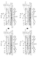
前記容器は、前記電子デバイスが搭載された第1面および前記第1面とは反対側の第2面を有する基部と、空間を介して前記電子デバイスに対向する対向部と、前記基部と前記対向部との間の前記空間を囲む枠部と、前記第2面の側において少なくとも前記電子デバイスの正射影領域に位置し、配線部材へはんだ付けされる複数の接続部と、を有しており、
前記第2面が凹面を成すように、前記基部の厚さは前記電子デバイスの正射影領域のうちの周辺領域よりも中央領域において小さくなっていることを特徴とする電子部品。 - 前記第1面が前記第2面よりも平坦である、請求項1に記載の電子部品。
- 前記第1面が凹面を成している、請求項1または2に記載の電子部品。
- 前記基部の厚さは前記周辺領域から前記中央領域に向かって連続的に小さくなっている、請求項1乃至3のいずれか1項に記載の電子部品。
- 前記基部は樹脂からなる、請求項1乃至4のいずれか1項に記載の電子部品。
- 前記電子部品の厚さは前記電子デバイスの正射影領域のうちの周辺領域よりも中央領域において小さくなっている、請求項1乃至5のいずれか1項に記載の電子部品。
- 前記電子デバイスは撮像デバイスまたは表示デバイスである、請求項1乃至6のいずれか1項に記載の電子部品。
- 請求項1乃至7のいずれか1項に記載の電子部品の前記複数の接続部と配線部材とを、リフローはんだ付けによって接合することを特徴とする電子モジュールの製造方法。
- 前記接合の後の前記第2面は前記接合の前の前記第2面よりも平坦である、請求項8に記載の電子モジュールの製造方法。
- 前記接合の後の前記第1面は凹面を成す、請求項8または9に記載の電子モジュールの製造方法。
Priority Applications (2)
| Application Number | Priority Date | Filing Date | Title |
|---|---|---|---|
| JP2015120405A JP6555942B2 (ja) | 2015-06-15 | 2015-06-15 | 電子モジュールの製造方法 |
| US15/177,250 US20160366774A1 (en) | 2015-06-15 | 2016-06-08 | Electronic component and method for manufacturing electronic module |
Applications Claiming Priority (1)
| Application Number | Priority Date | Filing Date | Title |
|---|---|---|---|
| JP2015120405A JP6555942B2 (ja) | 2015-06-15 | 2015-06-15 | 電子モジュールの製造方法 |
Publications (2)
| Publication Number | Publication Date |
|---|---|
| JP2017005199A true JP2017005199A (ja) | 2017-01-05 |
| JP6555942B2 JP6555942B2 (ja) | 2019-08-07 |
Family
ID=57517622
Family Applications (1)
| Application Number | Title | Priority Date | Filing Date |
|---|---|---|---|
| JP2015120405A Active JP6555942B2 (ja) | 2015-06-15 | 2015-06-15 | 電子モジュールの製造方法 |
Country Status (2)
| Country | Link |
|---|---|
| US (1) | US20160366774A1 (ja) |
| JP (1) | JP6555942B2 (ja) |
Cited By (1)
| Publication number | Priority date | Publication date | Assignee | Title |
|---|---|---|---|---|
| WO2020003647A1 (ja) * | 2018-06-29 | 2020-01-02 | ソニーセミコンダクタソリューションズ株式会社 | 撮像装置および撮像装置の製造方法 |
Families Citing this family (2)
| Publication number | Priority date | Publication date | Assignee | Title |
|---|---|---|---|---|
| CN109166839B (zh) * | 2018-08-30 | 2020-06-16 | 业成科技(成都)有限公司 | 接合垫的区域结构 |
| CN115939116A (zh) * | 2022-11-29 | 2023-04-07 | 友达光电股份有限公司 | 显示装置及其制造方法 |
Citations (7)
| Publication number | Priority date | Publication date | Assignee | Title |
|---|---|---|---|---|
| JPH0595060U (ja) * | 1992-05-29 | 1993-12-24 | 京セラ株式会社 | Ccd素子収納用パッケージ |
| JP2000164757A (ja) * | 1998-11-26 | 2000-06-16 | Kyocera Corp | 半導体素子収納用パッケージおよびその実装構造 |
| US6750549B1 (en) * | 2002-12-31 | 2004-06-15 | Intel Corporation | Variable pad diameter on the land side for improving the co-planarity of ball grid array packages |
| JP2006005071A (ja) * | 2004-06-16 | 2006-01-05 | Matsushita Electric Ind Co Ltd | 半導体装置用パッケージおよび半導体装置ならびに半導体装置用パッケージの製造方法 |
| JP2007266380A (ja) * | 2006-03-29 | 2007-10-11 | Matsushita Electric Ind Co Ltd | 半導体撮像装置およびその製造方法 |
| JP2008294960A (ja) * | 2007-05-28 | 2008-12-04 | Kyocera Corp | 撮像部品および撮像ユニット、ならびにこれらの製造方法 |
| JP2013243339A (ja) * | 2012-04-27 | 2013-12-05 | Canon Inc | 電子部品、電子モジュールおよびこれらの製造方法。 |
Family Cites Families (7)
| Publication number | Priority date | Publication date | Assignee | Title |
|---|---|---|---|---|
| JP3726998B2 (ja) * | 1999-04-01 | 2005-12-14 | 株式会社村田製作所 | 表面波装置 |
| JP2003188508A (ja) * | 2001-12-18 | 2003-07-04 | Toshiba Corp | プリント配線板、面実装形回路部品および回路モジュール |
| EP1860694A1 (en) * | 2005-03-16 | 2007-11-28 | Yamaha Corporation | Semiconductor device, semiconductor device manufacturing method and cover frame |
| JP4719009B2 (ja) * | 2006-01-13 | 2011-07-06 | ルネサスエレクトロニクス株式会社 | 基板および半導体装置 |
| US8633051B2 (en) * | 2009-08-24 | 2014-01-21 | Semiconductor Energy Laboratory Co., Ltd. | Semiconductor device and method for manufacturing semiconductor device |
| JP5885690B2 (ja) * | 2012-04-27 | 2016-03-15 | キヤノン株式会社 | 電子部品および電子機器 |
| US8920934B2 (en) * | 2013-03-29 | 2014-12-30 | Intel Corporation | Hybrid solder and filled paste in microelectronic packaging |
-
2015
- 2015-06-15 JP JP2015120405A patent/JP6555942B2/ja active Active
-
2016
- 2016-06-08 US US15/177,250 patent/US20160366774A1/en not_active Abandoned
Patent Citations (7)
| Publication number | Priority date | Publication date | Assignee | Title |
|---|---|---|---|---|
| JPH0595060U (ja) * | 1992-05-29 | 1993-12-24 | 京セラ株式会社 | Ccd素子収納用パッケージ |
| JP2000164757A (ja) * | 1998-11-26 | 2000-06-16 | Kyocera Corp | 半導体素子収納用パッケージおよびその実装構造 |
| US6750549B1 (en) * | 2002-12-31 | 2004-06-15 | Intel Corporation | Variable pad diameter on the land side for improving the co-planarity of ball grid array packages |
| JP2006005071A (ja) * | 2004-06-16 | 2006-01-05 | Matsushita Electric Ind Co Ltd | 半導体装置用パッケージおよび半導体装置ならびに半導体装置用パッケージの製造方法 |
| JP2007266380A (ja) * | 2006-03-29 | 2007-10-11 | Matsushita Electric Ind Co Ltd | 半導体撮像装置およびその製造方法 |
| JP2008294960A (ja) * | 2007-05-28 | 2008-12-04 | Kyocera Corp | 撮像部品および撮像ユニット、ならびにこれらの製造方法 |
| JP2013243339A (ja) * | 2012-04-27 | 2013-12-05 | Canon Inc | 電子部品、電子モジュールおよびこれらの製造方法。 |
Cited By (2)
| Publication number | Priority date | Publication date | Assignee | Title |
|---|---|---|---|---|
| WO2020003647A1 (ja) * | 2018-06-29 | 2020-01-02 | ソニーセミコンダクタソリューションズ株式会社 | 撮像装置および撮像装置の製造方法 |
| US12034029B2 (en) | 2018-06-29 | 2024-07-09 | Sony Semiconductor Solutions Corporation | Imaging device and method for producing imaging device |
Also Published As
| Publication number | Publication date |
|---|---|
| US20160366774A1 (en) | 2016-12-15 |
| JP6555942B2 (ja) | 2019-08-07 |
Similar Documents
| Publication | Publication Date | Title |
|---|---|---|
| US10910326B2 (en) | Semiconductor package | |
| US11728447B2 (en) | Semiconductor device and imaging apparatus | |
| US20070145403A1 (en) | Luminescent device and method for manufacturing the same | |
| US9509890B2 (en) | Solid image pickup apparatus | |
| JP6555942B2 (ja) | 電子モジュールの製造方法 | |
| KR20160024744A (ko) | Rf 전력 증폭기 모듈의 제조 방법과 rf 전력 증폭기 모듈, rf 모듈 및 기지국 | |
| CN108900174A (zh) | 一种石英晶体振荡器及制造该石英晶体振荡器的方法 | |
| JP5858637B2 (ja) | 半導体パッケージ | |
| JP2015188004A (ja) | パッケージ、半導体装置及び半導体モジュール | |
| JP6406121B2 (ja) | 高周波高出力デバイス | |
| JP4380442B2 (ja) | 半導体装置の製造方法 | |
| US20210273004A1 (en) | Imaging device and method for producing imaging device | |
| JP2014175567A (ja) | セラミックパッケージ | |
| KR20140098797A (ko) | 전자 부품 및 그 제조 방법 | |
| TWI393227B (zh) | 已封裝之積體電路及形成堆疊式積體電路封裝之方法 | |
| JP2004146466A (ja) | 蓋体およびこれを用いた光デバイス収納用パッケージ | |
| US20070235858A1 (en) | Mounting assembly for semiconductor devices | |
| JP2015056540A (ja) | 半導体装置及びその製造方法 | |
| JP4833678B2 (ja) | 圧電発振器の製造方法 | |
| JP2013140876A (ja) | 電子デバイスの製造方法、電子デバイス、圧電発振器、及び電子機器 | |
| JP2017028131A (ja) | パッケージ実装体 | |
| JP2004031815A (ja) | 蓋体およびこれを用いた光デバイス収納用パッケージ | |
| JP3734225B1 (ja) | 面実装タイプ樹脂製中空パッケージ及びこれを用いた半導体装置 | |
| JPWO2020045563A1 (ja) | 半導体パッケージおよびこれを備えた半導体装置 | |
| JPH0437137A (ja) | 半導体チップ又は半導体装置及びその製造方法 |
Legal Events
| Date | Code | Title | Description |
|---|---|---|---|
| A621 | Written request for application examination |
Free format text: JAPANESE INTERMEDIATE CODE: A621 Effective date: 20180525 |
|
| A977 | Report on retrieval |
Free format text: JAPANESE INTERMEDIATE CODE: A971007 Effective date: 20190118 |
|
| A131 | Notification of reasons for refusal |
Free format text: JAPANESE INTERMEDIATE CODE: A131 Effective date: 20190129 |
|
| A521 | Request for written amendment filed |
Free format text: JAPANESE INTERMEDIATE CODE: A523 Effective date: 20190311 |
|
| TRDD | Decision of grant or rejection written | ||
| A01 | Written decision to grant a patent or to grant a registration (utility model) |
Free format text: JAPANESE INTERMEDIATE CODE: A01 Effective date: 20190611 |
|
| A61 | First payment of annual fees (during grant procedure) |
Free format text: JAPANESE INTERMEDIATE CODE: A61 Effective date: 20190709 |
|
| R151 | Written notification of patent or utility model registration |
Ref document number: 6555942 Country of ref document: JP Free format text: JAPANESE INTERMEDIATE CODE: R151 |