JP2017011000A - 半導体装置および半導体装置の製造方法 - Google Patents
半導体装置および半導体装置の製造方法 Download PDFInfo
- Publication number
- JP2017011000A JP2017011000A JP2015122469A JP2015122469A JP2017011000A JP 2017011000 A JP2017011000 A JP 2017011000A JP 2015122469 A JP2015122469 A JP 2015122469A JP 2015122469 A JP2015122469 A JP 2015122469A JP 2017011000 A JP2017011000 A JP 2017011000A
- Authority
- JP
- Japan
- Prior art keywords
- region
- semiconductor device
- lifetime
- layer
- semiconductor substrate
- Prior art date
- Legal status (The legal status is an assumption and is not a legal conclusion. Google has not performed a legal analysis and makes no representation as to the accuracy of the status listed.)
- Granted
Links
Images








Classifications
-
- H—ELECTRICITY
- H10—SEMICONDUCTOR DEVICES; ELECTRIC SOLID-STATE DEVICES NOT OTHERWISE PROVIDED FOR
- H10D—INORGANIC ELECTRIC SEMICONDUCTOR DEVICES
- H10D8/00—Diodes
- H10D8/01—Manufacture or treatment
- H10D8/045—Manufacture or treatment of PN junction diodes
-
- H—ELECTRICITY
- H10—SEMICONDUCTOR DEVICES; ELECTRIC SOLID-STATE DEVICES NOT OTHERWISE PROVIDED FOR
- H10D—INORGANIC ELECTRIC SEMICONDUCTOR DEVICES
- H10D62/00—Semiconductor bodies, or regions thereof, of devices having potential barriers
- H10D62/10—Shapes, relative sizes or dispositions of the regions of the semiconductor bodies; Shapes of the semiconductor bodies
- H10D62/102—Constructional design considerations for preventing surface leakage or controlling electric field concentration
- H10D62/112—Constructional design considerations for preventing surface leakage or controlling electric field concentration for preventing surface leakage due to surface inversion layers, e.g. by using channel stoppers
-
- H—ELECTRICITY
- H10—SEMICONDUCTOR DEVICES; ELECTRIC SOLID-STATE DEVICES NOT OTHERWISE PROVIDED FOR
- H10D—INORGANIC ELECTRIC SEMICONDUCTOR DEVICES
- H10D12/00—Bipolar devices controlled by the field effect, e.g. insulated-gate bipolar transistors [IGBT]
- H10D12/01—Manufacture or treatment
- H10D12/031—Manufacture or treatment of IGBTs
- H10D12/032—Manufacture or treatment of IGBTs of vertical IGBTs
- H10D12/038—Manufacture or treatment of IGBTs of vertical IGBTs having a recessed gate, e.g. trench-gate IGBTs
-
- H—ELECTRICITY
- H10—SEMICONDUCTOR DEVICES; ELECTRIC SOLID-STATE DEVICES NOT OTHERWISE PROVIDED FOR
- H10D—INORGANIC ELECTRIC SEMICONDUCTOR DEVICES
- H10D12/00—Bipolar devices controlled by the field effect, e.g. insulated-gate bipolar transistors [IGBT]
- H10D12/411—Insulated-gate bipolar transistors [IGBT]
- H10D12/441—Vertical IGBTs
- H10D12/461—Vertical IGBTs having non-planar surfaces, e.g. having trenches, recesses or pillars in the surfaces of the emitter, base or collector regions
- H10D12/481—Vertical IGBTs having non-planar surfaces, e.g. having trenches, recesses or pillars in the surfaces of the emitter, base or collector regions having gate structures on slanted surfaces, on vertical surfaces, or in grooves, e.g. trench gate IGBTs
-
- H—ELECTRICITY
- H10—SEMICONDUCTOR DEVICES; ELECTRIC SOLID-STATE DEVICES NOT OTHERWISE PROVIDED FOR
- H10D—INORGANIC ELECTRIC SEMICONDUCTOR DEVICES
- H10D62/00—Semiconductor bodies, or regions thereof, of devices having potential barriers
- H10D62/10—Shapes, relative sizes or dispositions of the regions of the semiconductor bodies; Shapes of the semiconductor bodies
- H10D62/13—Semiconductor regions connected to electrodes carrying current to be rectified, amplified or switched, e.g. source or drain regions
- H10D62/141—Anode or cathode regions of thyristors; Collector or emitter regions of gated bipolar-mode devices, e.g. of IGBTs
- H10D62/142—Anode regions of thyristors or collector regions of gated bipolar-mode devices
-
- H—ELECTRICITY
- H10—SEMICONDUCTOR DEVICES; ELECTRIC SOLID-STATE DEVICES NOT OTHERWISE PROVIDED FOR
- H10D—INORGANIC ELECTRIC SEMICONDUCTOR DEVICES
- H10D62/00—Semiconductor bodies, or regions thereof, of devices having potential barriers
- H10D62/50—Physical imperfections
- H10D62/53—Physical imperfections the imperfections being within the semiconductor body
-
- H—ELECTRICITY
- H10—SEMICONDUCTOR DEVICES; ELECTRIC SOLID-STATE DEVICES NOT OTHERWISE PROVIDED FOR
- H10D—INORGANIC ELECTRIC SEMICONDUCTOR DEVICES
- H10D62/00—Semiconductor bodies, or regions thereof, of devices having potential barriers
- H10D62/80—Semiconductor bodies, or regions thereof, of devices having potential barriers characterised by the materials
- H10D62/83—Semiconductor bodies, or regions thereof, of devices having potential barriers characterised by the materials being Group IV materials, e.g. B-doped Si or undoped Ge
- H10D62/834—Semiconductor bodies, or regions thereof, of devices having potential barriers characterised by the materials being Group IV materials, e.g. B-doped Si or undoped Ge further characterised by the dopants
-
- H—ELECTRICITY
- H10—SEMICONDUCTOR DEVICES; ELECTRIC SOLID-STATE DEVICES NOT OTHERWISE PROVIDED FOR
- H10D—INORGANIC ELECTRIC SEMICONDUCTOR DEVICES
- H10D64/00—Electrodes of devices having potential barriers
- H10D64/111—Field plates
- H10D64/117—Recessed field plates, e.g. trench field plates or buried field plates
-
- H—ELECTRICITY
- H10—SEMICONDUCTOR DEVICES; ELECTRIC SOLID-STATE DEVICES NOT OTHERWISE PROVIDED FOR
- H10D—INORGANIC ELECTRIC SEMICONDUCTOR DEVICES
- H10D8/00—Diodes
- H10D8/422—PN diodes having the PN junctions in mesas
-
- H—ELECTRICITY
- H10—SEMICONDUCTOR DEVICES; ELECTRIC SOLID-STATE DEVICES NOT OTHERWISE PROVIDED FOR
- H10D—INORGANIC ELECTRIC SEMICONDUCTOR DEVICES
- H10D84/00—Integrated devices formed in or on semiconductor substrates that comprise only semiconducting layers, e.g. on Si wafers or on GaAs-on-Si wafers
-
- H—ELECTRICITY
- H10—SEMICONDUCTOR DEVICES; ELECTRIC SOLID-STATE DEVICES NOT OTHERWISE PROVIDED FOR
- H10D—INORGANIC ELECTRIC SEMICONDUCTOR DEVICES
- H10D84/00—Integrated devices formed in or on semiconductor substrates that comprise only semiconducting layers, e.g. on Si wafers or on GaAs-on-Si wafers
- H10D84/01—Manufacture or treatment
- H10D84/0123—Integrating together multiple components covered by H10D12/00 or H10D30/00, e.g. integrating multiple IGBTs
- H10D84/0126—Integrating together multiple components covered by H10D12/00 or H10D30/00, e.g. integrating multiple IGBTs the components including insulated gates, e.g. IGFETs
-
- H—ELECTRICITY
- H10—SEMICONDUCTOR DEVICES; ELECTRIC SOLID-STATE DEVICES NOT OTHERWISE PROVIDED FOR
- H10D—INORGANIC ELECTRIC SEMICONDUCTOR DEVICES
- H10D84/00—Integrated devices formed in or on semiconductor substrates that comprise only semiconducting layers, e.g. on Si wafers or on GaAs-on-Si wafers
- H10D84/01—Manufacture or treatment
- H10D84/02—Manufacture or treatment characterised by using material-based technologies
- H10D84/03—Manufacture or treatment characterised by using material-based technologies using Group IV technology, e.g. silicon technology or silicon-carbide [SiC] technology
- H10D84/038—Manufacture or treatment characterised by using material-based technologies using Group IV technology, e.g. silicon technology or silicon-carbide [SiC] technology using silicon technology, e.g. SiGe
-
- H—ELECTRICITY
- H10—SEMICONDUCTOR DEVICES; ELECTRIC SOLID-STATE DEVICES NOT OTHERWISE PROVIDED FOR
- H10D—INORGANIC ELECTRIC SEMICONDUCTOR DEVICES
- H10D84/00—Integrated devices formed in or on semiconductor substrates that comprise only semiconducting layers, e.g. on Si wafers or on GaAs-on-Si wafers
- H10D84/60—Integrated devices formed in or on semiconductor substrates that comprise only semiconducting layers, e.g. on Si wafers or on GaAs-on-Si wafers characterised by the integration of at least one component covered by groups H10D10/00 or H10D18/00, e.g. integration of BJTs
- H10D84/611—Combinations of BJTs and one or more of diodes, resistors or capacitors
- H10D84/613—Combinations of vertical BJTs and one or more of diodes, resistors or capacitors
- H10D84/617—Combinations of vertical BJTs and only diodes
-
- H—ELECTRICITY
- H10—SEMICONDUCTOR DEVICES; ELECTRIC SOLID-STATE DEVICES NOT OTHERWISE PROVIDED FOR
- H10D—INORGANIC ELECTRIC SEMICONDUCTOR DEVICES
- H10D84/00—Integrated devices formed in or on semiconductor substrates that comprise only semiconducting layers, e.g. on Si wafers or on GaAs-on-Si wafers
- H10D84/80—Integrated devices formed in or on semiconductor substrates that comprise only semiconducting layers, e.g. on Si wafers or on GaAs-on-Si wafers characterised by the integration of at least one component covered by groups H10D12/00 or H10D30/00, e.g. integration of IGFETs
- H10D84/82—Integrated devices formed in or on semiconductor substrates that comprise only semiconducting layers, e.g. on Si wafers or on GaAs-on-Si wafers characterised by the integration of at least one component covered by groups H10D12/00 or H10D30/00, e.g. integration of IGFETs of only field-effect components
- H10D84/83—Integrated devices formed in or on semiconductor substrates that comprise only semiconducting layers, e.g. on Si wafers or on GaAs-on-Si wafers characterised by the integration of at least one component covered by groups H10D12/00 or H10D30/00, e.g. integration of IGFETs of only field-effect components of only insulated-gate FETs [IGFET]
-
- H—ELECTRICITY
- H10—SEMICONDUCTOR DEVICES; ELECTRIC SOLID-STATE DEVICES NOT OTHERWISE PROVIDED FOR
- H10P—GENERIC PROCESSES OR APPARATUS FOR THE MANUFACTURE OR TREATMENT OF DEVICES COVERED BY CLASS H10
- H10P30/00—Ion implantation into wafers, substrates or parts of devices
- H10P30/20—Ion implantation into wafers, substrates or parts of devices into semiconductor materials, e.g. for doping
- H10P30/202—Ion implantation into wafers, substrates or parts of devices into semiconductor materials, e.g. for doping characterised by the semiconductor materials
- H10P30/204—Ion implantation into wafers, substrates or parts of devices into semiconductor materials, e.g. for doping characterised by the semiconductor materials into Group IV semiconductors
-
- H—ELECTRICITY
- H10—SEMICONDUCTOR DEVICES; ELECTRIC SOLID-STATE DEVICES NOT OTHERWISE PROVIDED FOR
- H10P—GENERIC PROCESSES OR APPARATUS FOR THE MANUFACTURE OR TREATMENT OF DEVICES COVERED BY CLASS H10
- H10P30/00—Ion implantation into wafers, substrates or parts of devices
- H10P30/20—Ion implantation into wafers, substrates or parts of devices into semiconductor materials, e.g. for doping
- H10P30/208—Ion implantation into wafers, substrates or parts of devices into semiconductor materials, e.g. for doping of electrically inactive species
-
- H—ELECTRICITY
- H10—SEMICONDUCTOR DEVICES; ELECTRIC SOLID-STATE DEVICES NOT OTHERWISE PROVIDED FOR
- H10P—GENERIC PROCESSES OR APPARATUS FOR THE MANUFACTURE OR TREATMENT OF DEVICES COVERED BY CLASS H10
- H10P30/00—Ion implantation into wafers, substrates or parts of devices
- H10P30/20—Ion implantation into wafers, substrates or parts of devices into semiconductor materials, e.g. for doping
- H10P30/21—Ion implantation into wafers, substrates or parts of devices into semiconductor materials, e.g. for doping of electrically active species
-
- H—ELECTRICITY
- H10—SEMICONDUCTOR DEVICES; ELECTRIC SOLID-STATE DEVICES NOT OTHERWISE PROVIDED FOR
- H10P—GENERIC PROCESSES OR APPARATUS FOR THE MANUFACTURE OR TREATMENT OF DEVICES COVERED BY CLASS H10
- H10P32/00—Diffusion of dopants within, into or out of wafers, substrates or parts of devices
- H10P32/10—Diffusion of dopants within, into or out of semiconductor bodies or layers
- H10P32/14—Diffusion of dopants within, into or out of semiconductor bodies or layers within a single semiconductor body or layer in a solid phase; between different semiconductor bodies or layers, both in a solid phase
- H10P32/1404—Diffusion of dopants within, into or out of semiconductor bodies or layers within a single semiconductor body or layer in a solid phase; between different semiconductor bodies or layers, both in a solid phase using predeposition followed by drive-in of impurities into the semiconductor surface, e.g. predeposition from a gaseous phase
- H10P32/1406—Diffusion of dopants within, into or out of semiconductor bodies or layers within a single semiconductor body or layer in a solid phase; between different semiconductor bodies or layers, both in a solid phase using predeposition followed by drive-in of impurities into the semiconductor surface, e.g. predeposition from a gaseous phase by ion implantation
-
- H—ELECTRICITY
- H10—SEMICONDUCTOR DEVICES; ELECTRIC SOLID-STATE DEVICES NOT OTHERWISE PROVIDED FOR
- H10P—GENERIC PROCESSES OR APPARATUS FOR THE MANUFACTURE OR TREATMENT OF DEVICES COVERED BY CLASS H10
- H10P32/00—Diffusion of dopants within, into or out of wafers, substrates or parts of devices
- H10P32/10—Diffusion of dopants within, into or out of semiconductor bodies or layers
- H10P32/17—Diffusion of dopants within, into or out of semiconductor bodies or layers characterised by the semiconductor material
- H10P32/171—Diffusion of dopants within, into or out of semiconductor bodies or layers characterised by the semiconductor material being group IV material
-
- H—ELECTRICITY
- H10—SEMICONDUCTOR DEVICES; ELECTRIC SOLID-STATE DEVICES NOT OTHERWISE PROVIDED FOR
- H10P—GENERIC PROCESSES OR APPARATUS FOR THE MANUFACTURE OR TREATMENT OF DEVICES COVERED BY CLASS H10
- H10P32/00—Diffusion of dopants within, into or out of wafers, substrates or parts of devices
- H10P32/10—Diffusion of dopants within, into or out of semiconductor bodies or layers
- H10P32/18—Diffusion lifetime killers
-
- H—ELECTRICITY
- H10—SEMICONDUCTOR DEVICES; ELECTRIC SOLID-STATE DEVICES NOT OTHERWISE PROVIDED FOR
- H10P—GENERIC PROCESSES OR APPARATUS FOR THE MANUFACTURE OR TREATMENT OF DEVICES COVERED BY CLASS H10
- H10P95/00—Generic processes or apparatus for manufacture or treatments not covered by the other groups of this subclass
- H10P95/90—Thermal treatments, e.g. annealing or sintering
-
- H—ELECTRICITY
- H10—SEMICONDUCTOR DEVICES; ELECTRIC SOLID-STATE DEVICES NOT OTHERWISE PROVIDED FOR
- H10D—INORGANIC ELECTRIC SEMICONDUCTOR DEVICES
- H10D62/00—Semiconductor bodies, or regions thereof, of devices having potential barriers
- H10D62/10—Shapes, relative sizes or dispositions of the regions of the semiconductor bodies; Shapes of the semiconductor bodies
- H10D62/17—Semiconductor regions connected to electrodes not carrying current to be rectified, amplified or switched, e.g. channel regions
- H10D62/393—Body regions of DMOS transistors or IGBTs
Landscapes
- Metal-Oxide And Bipolar Metal-Oxide Semiconductor Integrated Circuits (AREA)
- Thyristors (AREA)
Abstract
Description
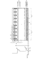
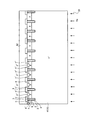
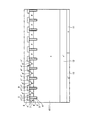
実施の形態にかかる半導体装置の製造方法により作製(製造)される半導体装置について説明する。図1は、実施の形態にかかる半導体装置の製造方法により製造される半導体装置の構成を示す断面図である。図1に示す実施の形態にかかる半導体装置は、n-型ドリフト層1となる同一のn-型半導体基板上に、絶縁ゲート型バイポーラトランジスタ(IGBT)が設けられたIGBT部21と、還流用ダイオード(FWD)が設けられたFWD部22と、を備える。FWD部22のFWDは、IGBT部21のIGBTに逆並列に接続されている。すなわち、図1に示す実施の形態にかかる半導体装置は、逆導通型IGBT(RC−IGBT)である。
2 p型ベース層
3 トレンチ
4 ゲート酸化膜
5 ゲート電極
6 n+型エミッタ領域
7 p+型コンタクト領域
8 エミッタ電極
9 層間絶縁膜
10 p+型コレクタ領域
11 n+型カソード領域
12 n+型FS層
13 コレクタ電極
20 MOSゲート構造
21 IGBT部
22 FWD部
31 第1低ライフタイム領域
32 第2低ライフタイム領域
Claims (14)
- 第1導電型のドリフト層を有する半導体基板、前記半導体基板のおもて面側に設けられた第2導電型のベース層、前記ベース層内に選択的に設けられた第1導電型のエミッタ領域、前記半導体基板のおもて面側に設けられたゲート絶縁膜およびゲート電極を備えた絶縁ゲート部、前記ベース層と前記エミッタ領域との両方に電気的に接続するエミッタ電極、前記半導体基板の裏面側に選択的に設けられた第2導電型のコレクタ領域、および前記コレクタ領域に電気的に接続するコレクタ電極を備えた絶縁ゲート型バイポーラトランジスタ部と、前記半導体基板のおもて面側に設けられ、かつ前記エミッタ電極に電気的に接続する第2導電型のアノード層、および前記半導体基板の裏面側に選択的に設けられ、かつ前記コレクタ電極に電気的に接続する第1導電型のカソード領域を備えた還流用ダイオード部と、を備えた半導体装置の製造方法であって、
前記半導体基板の裏面に第1導電型不純物を導入する導入工程と、
前記第1導電型不純物を熱処理により活性化させ、前記半導体基板の裏面から前記コレクタ領域よりも深い位置に、前記ドリフト層よりも不純物濃度が高い第1導電型のフィールドストップ層を形成する第1熱処理工程と、
前記半導体基板の裏面から軽イオンを照射し、前記ドリフト層内に他の領域よりもキャリアのライフタイムが短い第1低ライフタイム領域を形成する第1照射工程と、
前記半導体基板の裏面から軽イオンを照射し、前記フィールドストップ層内に他の領域よりもキャリアのライフタイムが短い第2低ライフタイム領域を形成する第2照射工程と、
前記第2照射工程で前記フィールドストップ層内に生じた欠陥の欠陥密度を熱処理により低減する第2熱処理工程と、
を含むことを特徴とする半導体装置の製造方法。 - 前記導入工程では、前記第1導電型不純物としてセレンを導入することを特徴とする請求項1に記載の半導体装置の製造方法。
- 前記第2熱処理工程では、前記フィールドストップ層内に形成された欠陥の欠陥密度を低減するとともに、前記フィールドストップ層内の軽イオンをドナー化させることを特徴とする請求項1または2に記載の半導体装置の製造方法。
- 前記第2熱処理工程は、350℃〜370℃の温度で1時間〜2時間行うことを特徴とする請求項1〜3のいずれか一つに記載の半導体装置の製造方法。
- 前記第2低ライフタイム領域のライフタイムを、前記第1低ライフタイム領域のライフタイムよりも短くすることを特徴とする請求項1〜4のいずれか一つに記載の半導体装置の製造方法。
- 前記軽イオンは、ヘリウムまたはプロトンであることを特徴とする請求項1〜5のいずれか一つに記載の半導体装置の製造方法。
- 第1導電型のドリフト層を有する半導体基板、前記半導体基板のおもて面側に設けられた第2導電型のベース層、前記ベース層内に選択的に設けられた第1導電型のエミッタ領域、前記半導体基板のおもて面側に設けられたゲート絶縁膜およびゲート電極を備えた絶縁ゲート部、前記ベース層と前記エミッタ領域との両方に電気的に接続するエミッタ電極、前記半導体基板の裏面側に選択的に設けられた第2導電型のコレクタ領域、および前記コレクタ領域に電気的に接続するコレクタ電極を備えた絶縁ゲート型バイポーラトランジスタ部と、
前記半導体基板のおもて面側に設けられ、かつ前記エミッタ電極に電気的に接続する第2導電型のアノード層、および前記半導体基板の裏面側に選択的に設けられ、かつ前記コレクタ電極に電気的に接続する第1導電型のカソード領域を備えた還流用ダイオード部と、
前記半導体基板の裏面から前記コレクタ領域よりも深い位置に設けられた、前記ドリフト層よりも不純物濃度が高い第1導電型のフィールドストップ層と、
前記ドリフト層内に前記フィールドストップ層と離れて設けられた、他の領域よりもキャリアのライフタイムが短い第1低ライフタイム領域と、
前記フィールドストップ層内に設けられた、他の領域よりもキャリアのライフタイムが短い第2低ライフタイム領域と、
を備えることを特徴とする半導体装置。 - 前記フィールドストップ層は、ドーパントとしてセレンを含むことを特徴とする請求項7に記載の半導体装置。
- 前記第1低ライフタイム領域は、軽イオンを含むことを特徴とする請求項7または8に記載の半導体装置。
- 前記第2低ライフタイム領域は、軽イオンを含むことを特徴とする請求項7〜9のいずれか一つに記載の半導体装置。
- 前記第2低ライフタイム領域に、軽イオンがドナー化されてなる領域が設けられていることを特徴とする請求項10に記載の半導体装置。
- 前記軽イオンは、ヘリウムかプロトンであることを特徴とする請求項9〜11のいずれか一つに記載の半導体装置。
- 前記第2低ライフタイム領域のライフタイムは、前記第1低ライフタイム領域のライフタイムよりも短いことを特徴とする請求項7〜12のいずれか一つに記載の半導体装置。
- 前記絶縁ゲート部は、
前記ベース層および前記エミッタ領域を貫通して前記ドリフト層に達するトレンチと、
前記トレンチの内壁に沿って設けられた前記ゲート絶縁膜と、
前記トレンチの内部に、前記ゲート絶縁膜を介して設けられた前記ゲート電極と、
を備えることを特徴とする請求項7〜13のいずれか一つに記載の半導体装置。
Priority Applications (4)
| Application Number | Priority Date | Filing Date | Title |
|---|---|---|---|
| JP2015122469A JP6272799B2 (ja) | 2015-06-17 | 2015-06-17 | 半導体装置および半導体装置の製造方法 |
| PCT/JP2016/067456 WO2016204097A1 (ja) | 2015-06-17 | 2016-06-10 | 半導体装置および半導体装置の製造方法 |
| CN201680012544.7A CN107251205B (zh) | 2015-06-17 | 2016-06-10 | 半导体装置和半导体装置的制造方法 |
| US15/686,216 US10629678B2 (en) | 2015-06-17 | 2017-08-25 | Semiconductor device and method of manufacturing semiconductor device |
Applications Claiming Priority (1)
| Application Number | Priority Date | Filing Date | Title |
|---|---|---|---|
| JP2015122469A JP6272799B2 (ja) | 2015-06-17 | 2015-06-17 | 半導体装置および半導体装置の製造方法 |
Publications (2)
| Publication Number | Publication Date |
|---|---|
| JP2017011000A true JP2017011000A (ja) | 2017-01-12 |
| JP6272799B2 JP6272799B2 (ja) | 2018-01-31 |
Family
ID=57545839
Family Applications (1)
| Application Number | Title | Priority Date | Filing Date |
|---|---|---|---|
| JP2015122469A Active JP6272799B2 (ja) | 2015-06-17 | 2015-06-17 | 半導体装置および半導体装置の製造方法 |
Country Status (4)
| Country | Link |
|---|---|
| US (1) | US10629678B2 (ja) |
| JP (1) | JP6272799B2 (ja) |
| CN (1) | CN107251205B (ja) |
| WO (1) | WO2016204097A1 (ja) |
Cited By (11)
| Publication number | Priority date | Publication date | Assignee | Title |
|---|---|---|---|---|
| WO2018179798A1 (ja) * | 2017-03-29 | 2018-10-04 | 富士電機株式会社 | 半導体装置の製造方法 |
| WO2019012875A1 (ja) * | 2017-07-12 | 2019-01-17 | 富士電機株式会社 | 半導体装置の製造方法 |
| WO2020230900A1 (ja) * | 2019-05-16 | 2020-11-19 | 富士電機株式会社 | 半導体装置および半導体装置の製造方法 |
| JP2021182614A (ja) * | 2019-06-17 | 2021-11-25 | 富士電機株式会社 | 半導体装置および半導体装置の製造方法 |
| US11355595B2 (en) | 2019-01-18 | 2022-06-07 | Fuji Electric Co., Ltd. | Semiconductor device and method of manufacturing semiconductor device |
| DE112020003167T5 (de) | 2020-02-12 | 2022-06-30 | Fuji Electric Co., Ltd. | Halbleitervorrichtung und dessen herstellungsverfahren |
| JP2022105112A (ja) * | 2018-10-18 | 2022-07-12 | 富士電機株式会社 | 半導体装置および製造方法 |
| JP2022126856A (ja) * | 2018-12-28 | 2022-08-30 | 富士電機株式会社 | 半導体装置 |
| JP2022163554A (ja) * | 2021-04-14 | 2022-10-26 | 富士電機株式会社 | 炭化珪素半導体装置及びその製造方法 |
| WO2024009591A1 (ja) * | 2022-07-07 | 2024-01-11 | ローム株式会社 | 半導体装置および半導体装置の製造方法 |
| JP2024021099A (ja) * | 2022-08-03 | 2024-02-16 | 三菱電機株式会社 | 半導体装置及び半導体装置の製造方法 |
Families Citing this family (16)
| Publication number | Priority date | Publication date | Assignee | Title |
|---|---|---|---|---|
| CN105814694B (zh) * | 2014-10-03 | 2019-03-08 | 富士电机株式会社 | 半导体装置以及半导体装置的制造方法 |
| JP6903931B2 (ja) * | 2017-02-13 | 2021-07-14 | 富士電機株式会社 | 半導体装置および半導体装置の製造方法 |
| DE112018003666B4 (de) * | 2017-07-19 | 2025-02-06 | Mitsubishi Electric Corporation | Verfahren zur herstellung eines halbleiterbauelements und halbleiterbauelement |
| CN109979935B (zh) * | 2017-12-28 | 2025-04-22 | 富士电机株式会社 | 半导体装置及半导体装置的制造方法 |
| DE112019000094T5 (de) * | 2018-03-19 | 2020-09-24 | Fuji Electric Co., Ltd. | Halbleitervorrichtung und verfahren zum herstellen einerhalbleitervorrichtung |
| JP6958732B2 (ja) * | 2018-05-10 | 2021-11-02 | 富士電機株式会社 | 半導体装置の製造方法 |
| DE112020001029B4 (de) | 2019-10-11 | 2025-06-05 | Fuji Electric Co., Ltd. | Halbleitervorrichtung und herstellungsverfahren einer halbleitervorrichtung |
| WO2021232548A1 (zh) * | 2020-05-21 | 2021-11-25 | 华大半导体有限公司 | 功率半导体装置及其制备方法 |
| CN111900087B (zh) * | 2020-08-31 | 2022-09-20 | 华虹半导体(无锡)有限公司 | Igbt器件的制造方法 |
| CN114256066B (zh) * | 2020-09-22 | 2025-03-21 | 珠海格力电器股份有限公司 | 一种少子寿命控制方法 |
| CN116547788B (zh) | 2020-12-15 | 2025-02-18 | 三菱电机株式会社 | 半导体装置的制造方法以及半导体装置 |
| CN112397593B (zh) * | 2021-01-20 | 2021-04-16 | 中芯集成电路制造(绍兴)有限公司 | 半导体器件及制造方法 |
| CN113745328A (zh) * | 2021-08-31 | 2021-12-03 | 上海华虹挚芯电子科技有限公司 | Igbt器件的结构及工艺方法 |
| CN113851379A (zh) * | 2021-09-24 | 2021-12-28 | 上海积塔半导体有限公司 | Igbt器件及其制作方法 |
| CN114899147B (zh) * | 2022-07-12 | 2022-10-21 | 深圳芯能半导体技术有限公司 | 一种rc-igbt器件及其制备方法 |
| US20250380436A1 (en) * | 2024-06-11 | 2025-12-11 | Ideal Power Inc. | Methods of manufacturing bipolar junction devices |
Citations (6)
| Publication number | Priority date | Publication date | Assignee | Title |
|---|---|---|---|---|
| JPH1050724A (ja) * | 1996-07-30 | 1998-02-20 | Toshiba Corp | 半導体装置 |
| JP2011238872A (ja) * | 2010-05-13 | 2011-11-24 | Toyota Central R&D Labs Inc | 半導体装置 |
| JP2012043891A (ja) * | 2010-08-17 | 2012-03-01 | Denso Corp | 半導体装置 |
| JP2013074181A (ja) * | 2011-09-28 | 2013-04-22 | Toyota Motor Corp | 半導体装置とその製造方法 |
| JP2013138172A (ja) * | 2011-11-30 | 2013-07-11 | Denso Corp | 半導体装置 |
| JP2013247248A (ja) * | 2012-05-25 | 2013-12-09 | Fuji Electric Co Ltd | 半導体装置の製造方法 |
Family Cites Families (16)
| Publication number | Priority date | Publication date | Assignee | Title |
|---|---|---|---|---|
| CA2423323C (en) * | 2000-09-29 | 2009-12-01 | Forensic Technology Wai Inc. | Method and system for identification of firearms |
| JP4791704B2 (ja) | 2004-04-28 | 2011-10-12 | 三菱電機株式会社 | 逆導通型半導体素子とその製造方法 |
| JP5272299B2 (ja) | 2005-11-10 | 2013-08-28 | 富士電機株式会社 | 半導体装置およびその製造方法 |
| US7728409B2 (en) | 2005-11-10 | 2010-06-01 | Fuji Electric Device Technology Co., Ltd. | Semiconductor device and method of manufacturing the same |
| JP5228308B2 (ja) | 2006-10-19 | 2013-07-03 | 富士電機株式会社 | 半導体装置の製造方法 |
| JP5320679B2 (ja) | 2007-02-28 | 2013-10-23 | 富士電機株式会社 | 半導体装置およびその製造方法 |
| US7932583B2 (en) | 2008-05-13 | 2011-04-26 | Infineon Technologies Austria Ag | Reduced free-charge carrier lifetime device |
| JP4905559B2 (ja) * | 2009-01-27 | 2012-03-28 | 株式会社デンソー | 半導体装置 |
| EP2477226B1 (en) * | 2009-09-07 | 2016-06-22 | Toyota Jidosha Kabushiki Kaisha | Semiconductor device including semiconductor substrate having diode region and igbt region |
| JP5565134B2 (ja) | 2010-06-24 | 2014-08-06 | 富士電機株式会社 | 半導体装置の製造方法 |
| JP2012256628A (ja) * | 2011-06-07 | 2012-12-27 | Renesas Electronics Corp | Igbtおよびダイオード |
| US9627517B2 (en) * | 2013-02-07 | 2017-04-18 | Infineon Technologies Ag | Bipolar semiconductor switch and a manufacturing method therefor |
| JP2015008235A (ja) * | 2013-06-25 | 2015-01-15 | 富士電機株式会社 | 半導体装置の製造方法 |
| JP6037012B2 (ja) * | 2013-06-26 | 2016-11-30 | 富士電機株式会社 | 半導体装置および半導体装置の製造方法 |
| US9484221B2 (en) * | 2014-01-13 | 2016-11-01 | Infineon Technologies Ag | Bipolar semiconductor device and method of manufacturing thereof |
| JP2016162807A (ja) * | 2015-02-27 | 2016-09-05 | トヨタ自動車株式会社 | 半導体装置とその製造方法 |
-
2015
- 2015-06-17 JP JP2015122469A patent/JP6272799B2/ja active Active
-
2016
- 2016-06-10 WO PCT/JP2016/067456 patent/WO2016204097A1/ja not_active Ceased
- 2016-06-10 CN CN201680012544.7A patent/CN107251205B/zh active Active
-
2017
- 2017-08-25 US US15/686,216 patent/US10629678B2/en active Active
Patent Citations (6)
| Publication number | Priority date | Publication date | Assignee | Title |
|---|---|---|---|---|
| JPH1050724A (ja) * | 1996-07-30 | 1998-02-20 | Toshiba Corp | 半導体装置 |
| JP2011238872A (ja) * | 2010-05-13 | 2011-11-24 | Toyota Central R&D Labs Inc | 半導体装置 |
| JP2012043891A (ja) * | 2010-08-17 | 2012-03-01 | Denso Corp | 半導体装置 |
| JP2013074181A (ja) * | 2011-09-28 | 2013-04-22 | Toyota Motor Corp | 半導体装置とその製造方法 |
| JP2013138172A (ja) * | 2011-11-30 | 2013-07-11 | Denso Corp | 半導体装置 |
| JP2013247248A (ja) * | 2012-05-25 | 2013-12-09 | Fuji Electric Co Ltd | 半導体装置の製造方法 |
Cited By (28)
| Publication number | Priority date | Publication date | Assignee | Title |
|---|---|---|---|---|
| WO2018179798A1 (ja) * | 2017-03-29 | 2018-10-04 | 富士電機株式会社 | 半導体装置の製造方法 |
| JPWO2018179798A1 (ja) * | 2017-03-29 | 2019-07-04 | 富士電機株式会社 | 半導体装置の製造方法 |
| US10755933B2 (en) | 2017-03-29 | 2020-08-25 | Fuji Electric Co., Ltd. | Method of manufacturing semiconductor device |
| WO2019012875A1 (ja) * | 2017-07-12 | 2019-01-17 | 富士電機株式会社 | 半導体装置の製造方法 |
| JPWO2019012875A1 (ja) * | 2017-07-12 | 2019-11-07 | 富士電機株式会社 | 半導体装置の製造方法 |
| US10522355B2 (en) | 2017-07-12 | 2019-12-31 | Fuji Electric Co., Ltd. | Method of manufacturing semiconductor device |
| JP2022105112A (ja) * | 2018-10-18 | 2022-07-12 | 富士電機株式会社 | 半導体装置および製造方法 |
| US11735424B2 (en) | 2018-10-18 | 2023-08-22 | Fuji Electric Co., Ltd. | Semiconductor device and manufacturing method thereof |
| JP7487753B2 (ja) | 2018-10-18 | 2024-05-21 | 富士電機株式会社 | 半導体装置および製造方法 |
| JP7722487B2 (ja) | 2018-10-18 | 2025-08-13 | 富士電機株式会社 | 半導体装置および製造方法 |
| JP2024040283A (ja) * | 2018-10-18 | 2024-03-25 | 富士電機株式会社 | 半導体装置および製造方法 |
| US12191148B2 (en) | 2018-10-18 | 2025-01-07 | Fuji Electric Co., Ltd. | Semiconductor device and manufacturing method thereof |
| JP7563425B2 (ja) | 2018-12-28 | 2024-10-08 | 富士電機株式会社 | 半導体装置 |
| US12368048B2 (en) | 2018-12-28 | 2025-07-22 | Fuji Electric Co., Ltd. | Semiconductor device and method for manufacturing |
| JP2022126856A (ja) * | 2018-12-28 | 2022-08-30 | 富士電機株式会社 | 半導体装置 |
| US11972950B2 (en) | 2018-12-28 | 2024-04-30 | Fuji Electric Co., Ltd. | Semiconductor device and method for manufacturing |
| US11355595B2 (en) | 2019-01-18 | 2022-06-07 | Fuji Electric Co., Ltd. | Semiconductor device and method of manufacturing semiconductor device |
| US12349376B1 (en) | 2019-05-16 | 2025-07-01 | Fuji Electric Co., Ltd. | Semiconductor device and manufacturing method of semiconductor device |
| US11935945B2 (en) | 2019-05-16 | 2024-03-19 | Fuji Electric Co., Ltd. | Semiconductor device and manufacturing method of semiconductor device |
| WO2020230900A1 (ja) * | 2019-05-16 | 2020-11-19 | 富士電機株式会社 | 半導体装置および半導体装置の製造方法 |
| JP2021182614A (ja) * | 2019-06-17 | 2021-11-25 | 富士電機株式会社 | 半導体装置および半導体装置の製造方法 |
| US12009268B2 (en) | 2019-06-17 | 2024-06-11 | Fuji Electric Co., Ltd. | Semiconductor device and fabrication method for semiconductor device |
| US12283608B2 (en) | 2020-02-12 | 2025-04-22 | Fuji Electric Co., Ltd. | Semiconductor device and manufacturing method of the same |
| DE112020003167T5 (de) | 2020-02-12 | 2022-06-30 | Fuji Electric Co., Ltd. | Halbleitervorrichtung und dessen herstellungsverfahren |
| JP7703882B2 (ja) | 2021-04-14 | 2025-07-08 | 富士電機株式会社 | 炭化珪素半導体装置及びその製造方法 |
| JP2022163554A (ja) * | 2021-04-14 | 2022-10-26 | 富士電機株式会社 | 炭化珪素半導体装置及びその製造方法 |
| WO2024009591A1 (ja) * | 2022-07-07 | 2024-01-11 | ローム株式会社 | 半導体装置および半導体装置の製造方法 |
| JP2024021099A (ja) * | 2022-08-03 | 2024-02-16 | 三菱電機株式会社 | 半導体装置及び半導体装置の製造方法 |
Also Published As
| Publication number | Publication date |
|---|---|
| WO2016204097A1 (ja) | 2016-12-22 |
| CN107251205B (zh) | 2020-09-25 |
| US10629678B2 (en) | 2020-04-21 |
| US20170373141A1 (en) | 2017-12-28 |
| JP6272799B2 (ja) | 2018-01-31 |
| CN107251205A (zh) | 2017-10-13 |
Similar Documents
| Publication | Publication Date | Title |
|---|---|---|
| JP6272799B2 (ja) | 半導体装置および半導体装置の製造方法 | |
| JP6078961B2 (ja) | 半導体装置の製造方法 | |
| JP6662429B2 (ja) | 逆導通型絶縁ゲートバイポーラトランジスタの製造方法および逆導通型絶縁ゲートバイポーラトランジスタ | |
| JP5754545B2 (ja) | 半導体装置および半導体装置の製造方法 | |
| CN101494238B (zh) | 半导体装置 | |
| JP5641055B2 (ja) | 半導体装置およびその製造方法 | |
| CN103986447B (zh) | 双极半导体开关及其制造方法 | |
| JP6334465B2 (ja) | 半導体装置 | |
| JP6524666B2 (ja) | 半導体装置 | |
| JP3684962B2 (ja) | 半導体装置の製造方法 | |
| CN110600537B (zh) | 一种具有pmos电流嵌位的分离栅cstbt及其制作方法 | |
| WO2017047285A1 (ja) | 半導体装置および半導体装置の製造方法 | |
| JPWO2012056536A1 (ja) | 半導体装置および半導体装置の製造方法 | |
| JP2018078216A (ja) | 半導体装置およびその製造方法 | |
| JP2018152426A (ja) | 半導体装置 | |
| JP4910894B2 (ja) | 半導体装置の製造方法および半導体装置 | |
| WO2014086075A1 (zh) | 一种igbt结构及其制备方法 | |
| CN113451397A (zh) | 一种rc-igbt器件及其制备方法 | |
| JP6780335B2 (ja) | 逆阻止mos型半導体装置および逆阻止mos型半導体装置の製造方法 | |
| JP2012023327A (ja) | 半導体装置の製造方法 | |
| US12593483B2 (en) | Semiconductor device and method of manufacturing semiconductor device | |
| JP2015090953A (ja) | Mos型半導体装置の製造方法 | |
| CN121665598A (zh) | Igbt器件及其制造方法 | |
| JP2018041972A (ja) | 半導体装置 | |
| JPH10289999A (ja) | 絶縁ゲート型サイリスタ |
Legal Events
| Date | Code | Title | Description |
|---|---|---|---|
| A621 | Written request for application examination |
Free format text: JAPANESE INTERMEDIATE CODE: A621 Effective date: 20170614 |
|
| A131 | Notification of reasons for refusal |
Free format text: JAPANESE INTERMEDIATE CODE: A131 Effective date: 20170912 |
|
| A521 | Request for written amendment filed |
Free format text: JAPANESE INTERMEDIATE CODE: A523 Effective date: 20171113 |
|
| TRDD | Decision of grant or rejection written | ||
| A01 | Written decision to grant a patent or to grant a registration (utility model) |
Free format text: JAPANESE INTERMEDIATE CODE: A01 Effective date: 20171205 |
|
| A61 | First payment of annual fees (during grant procedure) |
Free format text: JAPANESE INTERMEDIATE CODE: A61 Effective date: 20180104 |
|
| R150 | Certificate of patent or registration of utility model |
Ref document number: 6272799 Country of ref document: JP Free format text: JAPANESE INTERMEDIATE CODE: R150 |
|
| R250 | Receipt of annual fees |
Free format text: JAPANESE INTERMEDIATE CODE: R250 |
|
| R250 | Receipt of annual fees |
Free format text: JAPANESE INTERMEDIATE CODE: R250 |
|
| R250 | Receipt of annual fees |
Free format text: JAPANESE INTERMEDIATE CODE: R250 |
|
| R250 | Receipt of annual fees |
Free format text: JAPANESE INTERMEDIATE CODE: R250 |
|
| R250 | Receipt of annual fees |
Free format text: JAPANESE INTERMEDIATE CODE: R250 |
|
| R250 | Receipt of annual fees |
Free format text: JAPANESE INTERMEDIATE CODE: R250 |