JP2017184185A - 撮像装置、撮像システム、および、移動体 - Google Patents
撮像装置、撮像システム、および、移動体 Download PDFInfo
- Publication number
- JP2017184185A JP2017184185A JP2016072990A JP2016072990A JP2017184185A JP 2017184185 A JP2017184185 A JP 2017184185A JP 2016072990 A JP2016072990 A JP 2016072990A JP 2016072990 A JP2016072990 A JP 2016072990A JP 2017184185 A JP2017184185 A JP 2017184185A
- Authority
- JP
- Japan
- Prior art keywords
- input node
- pixel
- signal
- capacitance
- output
- Prior art date
- Legal status (The legal status is an assumption and is not a legal conclusion. Google has not performed a legal analysis and makes no representation as to the accuracy of the status listed.)
- Granted
Links
Images




Classifications
-
- G—PHYSICS
- G06—COMPUTING OR CALCULATING; COUNTING
- G06T—IMAGE DATA PROCESSING OR GENERATION, IN GENERAL
- G06T7/00—Image analysis
- G06T7/70—Determining position or orientation of objects or cameras
- G06T7/73—Determining position or orientation of objects or cameras using feature-based methods
- G06T7/74—Determining position or orientation of objects or cameras using feature-based methods involving reference images or patches
-
- G—PHYSICS
- G05—CONTROLLING; REGULATING
- G05B—CONTROL OR REGULATING SYSTEMS IN GENERAL; FUNCTIONAL ELEMENTS OF SUCH SYSTEMS; MONITORING OR TESTING ARRANGEMENTS FOR SUCH SYSTEMS OR ELEMENTS
- G05B15/00—Systems controlled by a computer
- G05B15/02—Systems controlled by a computer electric
-
- H—ELECTRICITY
- H04—ELECTRIC COMMUNICATION TECHNIQUE
- H04N—PICTORIAL COMMUNICATION, e.g. TELEVISION
- H04N23/00—Cameras or camera modules comprising electronic image sensors; Control thereof
- H04N23/60—Control of cameras or camera modules
- H04N23/667—Camera operation mode switching, e.g. between still and video, sport and normal or high- and low-resolution modes
-
- H—ELECTRICITY
- H04—ELECTRIC COMMUNICATION TECHNIQUE
- H04N—PICTORIAL COMMUNICATION, e.g. TELEVISION
- H04N25/00—Circuitry of solid-state image sensors [SSIS]; Control thereof
- H04N25/40—Extracting pixel data from image sensors by controlling scanning circuits, e.g. by modifying the number of pixels sampled or to be sampled
- H04N25/44—Extracting pixel data from image sensors by controlling scanning circuits, e.g. by modifying the number of pixels sampled or to be sampled by partially reading an SSIS array
- H04N25/447—Extracting pixel data from image sensors by controlling scanning circuits, e.g. by modifying the number of pixels sampled or to be sampled by partially reading an SSIS array by preserving the colour pattern with or without loss of information
-
- H—ELECTRICITY
- H04—ELECTRIC COMMUNICATION TECHNIQUE
- H04N—PICTORIAL COMMUNICATION, e.g. TELEVISION
- H04N25/00—Circuitry of solid-state image sensors [SSIS]; Control thereof
- H04N25/70—SSIS architectures; Circuits associated therewith
- H04N25/703—SSIS architectures incorporating pixels for producing signals other than image signals
-
- H—ELECTRICITY
- H04—ELECTRIC COMMUNICATION TECHNIQUE
- H04N—PICTORIAL COMMUNICATION, e.g. TELEVISION
- H04N25/00—Circuitry of solid-state image sensors [SSIS]; Control thereof
- H04N25/70—SSIS architectures; Circuits associated therewith
- H04N25/76—Addressed sensors, e.g. MOS or CMOS sensors
- H04N25/77—Pixel circuitry, e.g. memories, A/D converters, pixel amplifiers, shared circuits or shared components
- H04N25/771—Pixel circuitry, e.g. memories, A/D converters, pixel amplifiers, shared circuits or shared components comprising storage means other than floating diffusion
-
- H—ELECTRICITY
- H04—ELECTRIC COMMUNICATION TECHNIQUE
- H04N—PICTORIAL COMMUNICATION, e.g. TELEVISION
- H04N25/00—Circuitry of solid-state image sensors [SSIS]; Control thereof
- H04N25/70—SSIS architectures; Circuits associated therewith
- H04N25/76—Addressed sensors, e.g. MOS or CMOS sensors
- H04N25/77—Pixel circuitry, e.g. memories, A/D converters, pixel amplifiers, shared circuits or shared components
- H04N25/778—Pixel circuitry, e.g. memories, A/D converters, pixel amplifiers, shared circuits or shared components comprising amplifiers shared between a plurality of pixels, i.e. at least one part of the amplifier must be on the sensor array itself
-
- H—ELECTRICITY
- H04—ELECTRIC COMMUNICATION TECHNIQUE
- H04N—PICTORIAL COMMUNICATION, e.g. TELEVISION
- H04N25/00—Circuitry of solid-state image sensors [SSIS]; Control thereof
- H04N25/70—SSIS architectures; Circuits associated therewith
- H04N25/76—Addressed sensors, e.g. MOS or CMOS sensors
- H04N25/78—Readout circuits for addressed sensors, e.g. output amplifiers or A/D converters
Landscapes
- Engineering & Computer Science (AREA)
- Multimedia (AREA)
- Signal Processing (AREA)
- Physics & Mathematics (AREA)
- General Physics & Mathematics (AREA)
- Computer Vision & Pattern Recognition (AREA)
- Theoretical Computer Science (AREA)
- General Engineering & Computer Science (AREA)
- Automation & Control Theory (AREA)
- Transforming Light Signals Into Electric Signals (AREA)
- Solid State Image Pick-Up Elements (AREA)
- Studio Devices (AREA)
Abstract
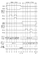
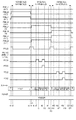
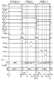
【解決手段】画素は101、光電変換で生じた電荷を受ける入力ノード205を有する増幅トランジスタ207、リセットトランジスタ206、容量制御部210を含む。リセットトランジスタがオフである状態で、容量制御部が入力ノードの容量211を第1の容量値C1から第1の容量値C1より大きい第2の容量値C2に切り替える。その後、入力ノードの容量がC2に制御された状態で、リセットトランジスタがオフからオンに制御される。当該リセット動作の後に、入力ノードの容量がC1である状態で増幅トランジスタが画素信号を出力する。
【選択図】図2
Description
図1は、第1の実施例に係る撮像装置の全体構成を模式的に示したブロック図である。画素部100に、複数の画素101が配置される。本実施例では、1つの画素101が1つの画素ユニットを構成する。複数の画素101は複数の行、および、複数の列を含む行列状に配されている。画素101は、光電変換により生じた電荷に基づく画素信号を出力する。それぞれの画素101に対して、赤R、緑G、または、青Bのいずれかのカラーフィルタが割り当てられる。したがって、配置されたカラーフィルタを透過する色を持つ光が画素101に入射する。複数のカラーフィルタが、通常、ベイヤー状に配置されている。
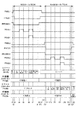
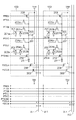
別の実施例を説明する。本実施形態は、1つの画素ユニットが複数の画素を含む点で実施例1と異なる。また、1つの画素ユニットに含まれる複数の画素は、画素ユニットに含まれる回路の一部を共有している。そのため、画素から画素信号を読み出すための動作が、実施例1と異なる。以下では実施例1と異なる部分を主に説明する。実施例1と同じ部分については、説明を省略する。
本発明に係る撮像システムの実施例について説明する。撮像システムとして、デジタルスチルカメラ、デジタルカムコーダ、カメラヘッド、複写機、ファックス、携帯電話、車載カメラ、観測衛星などがあげられる。図9に、撮像システムの例としてデジタルスチルカメラのブロック図を示す。
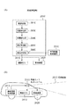
図10は、車戴カメラに関する撮像システムの一例を示したものである。撮像システム2000は、上述した実施例の撮像装置2010を有する。撮像システム2000は、撮像装置2010により取得された複数の画像データに対し、画像処理を行う画像処理部2030と、撮像システム2000により取得された複数の画像データから視差(視差画像の位相差)の算出を行う視差算出部2040を有する。また、撮像システム2000は、算出された視差に基づいて対象物までの距離を算出する距離計測部2050と、算出された距離に基づいて衝突可能性があるか否かを判定する衝突判定部2060と、を有する。ここで、視差算出部2040や距離計測部2050は、対象物までの距離情報を取得する距離情報取得手段の一例である。すなわち、距離情報とは、視差、デフォーカス量、対象物までの距離等に関する情報である。衝突判定部2060はこれらの距離情報のいずれかを用いて、衝突可能性を判定してもよい。距離情報取得手段は、専用に設計されたハードウェアによって実現されてもよいし、ソフトウェアモジュールによって実現されてもよい。また、FPGA(Field Programmable Gate Array)やASIC(Application Specific Integrated Circuit)などによって実現されてもよいし、これらの組合せによって実現されてもよい。
150 画素ユニット
205 入力ノード
206 リセットトランジスタ
207 増幅トランジスタ
210 容量制御部
Claims (13)
- 光電変換によって生じた電荷を受ける入力ノードを有し、前記入力ノードの電圧に基づく信号を出力する出力部と、
オンとオフとに制御され、前記オンのときに前記入力ノードの電圧をリセットするリセット部と、
制御信号を受けるゲート電極を有し、前記制御信号に応じて前記入力ノードの容量を第1の容量値と前記第1の容量値より大きい第2の容量値とに制御する制御部と、をそれぞれが含む複数の画素ユニットを備え、
前記入力ノードの容量が前記第1の容量値である状態で、前記出力部が前記信号を出力する第1のモードと、
前記入力ノードの容量が前記第2の容量値である状態で、前記出力部が前記信号を出力する第2のモードと、を有し、
前記第1のモードにおいて、
前記リセット部が前記オフである状態で、前記制御部が前記入力ノードの容量を前記第1の容量値から前記第2の容量値に切り替え、その後、前記入力ノードの容量が前記第2の容量値である状態で、前記リセット部が前記オフから前記オンに制御されるリセット動作と、
前記リセット動作の後に、前記入力ノードの容量が前記第1の容量値である状態で前記出力部が前記信号を出力する出力動作と、を行う、
ことを特徴とする撮像装置。 - 前記第2のモードにおいて、
前記入力ノードの容量が前記第2の容量値に制御された状態で前記リセット部が前記オフから前記オンに制御される第2のリセット動作と、
前記第2のリセット動作の後に、前記入力ノードの容量が前記第2の容量値である状態で前記出力部が前記信号を出力する第2の出力動作と、を行い、
前記第2のリセット動作から前記第2の出力動作までの間、前記入力ノードの容量が前記第2の容量値に維持される、
ことを特徴とする請求項1に記載の撮像装置。 - 前記複数の画素ユニットのそれぞれが、前記電荷を前記入力ノードに転送する転送部を備え、
前記出力動作は、
前記電荷が転送される前に、前記出力部が第1の信号を出力する第1の出力動作と、
前記電荷が転送された後に、前記出力部が第2の信号を出力する第2の出力動作と、を含む、
ことを特徴とする請求項1または請求項2に記載の撮像装置。 - 前記複数の画素ユニットのそれぞれが、複数の光電変換部を含み、
前記入力ノードが、前記複数の光電変換部のそれぞれで生じた電荷を受ける、
ことを特徴とする請求項1乃至請求項3のいずれか一項に記載の撮像装置。 - 前記複数の光電変換部が、単一のマイクロレンズの下に配される、
ことを特徴とする請求項4に記載の撮像装置。 - 前記複数の光電変換部それぞれで生じた電荷が、前記入力ノードにおいて加算される、
ことを特徴とする請求項5に記載の撮像装置。 - 前記複数の光電変換部のそれぞれが、互いに異なるマイクロレンズの下に配される、
ことを特徴とする請求項4に記載の撮像装置。 - 前記複数の画素ユニットは、前記複数の複数の列を構成するように配置され、
前記複数の列の1つに対応して、複数の出力線が配される、
ことを特徴とする請求項1乃至請求項7のいずれか一項に記載の撮像装置。 - 前記複数の出力線は、少なくとも第1の出力線と、第2の出力線とを含み、
前記複数の画素ユニットのそれぞれは、前記出力部と前記第1の出力線とを接続する第1の選択トランジスタと、前記出力部と前記第2の出力線とを接続する第2の選択トランジスタと、を含む、
ことを特徴とする請求項8に記載の撮像装置。 - 前記の出力線に対応した複数の列回路を含み、
前記複数の列回路の間に、前記複数の画素ユニットが配置される、
ことを特徴とする請求項8または請求項9に記載の撮像装置。 - 前記入力ノードを構成する第1導電型のフローティングディフュージョン領域と、
前記フローティングディフュージョン領域の隣に配された第2導電型の半導体領域と、を備え、
前記ゲート電極は、前記半導体領域の上に絶縁膜を介して配置される、
ことを特徴とする請求項1乃至請求項10のいずれか一項に記載の撮像装置。 - 請求項1乃至請求項11のいずれか一項に記載の撮像装置と、
前記撮像装置からの信号を処理する信号処理装置と、を備えた撮像システム。 - 移動体であって、
請求項1乃至12のいずれか一項に記載の撮像装置と、
前記撮像装置からの信号に基づく視差画像から、対象物までの距離情報を取得する距離情報取得手段と、
前記距離情報に基づいて前記移動体を制御する制御手段と、を有することを特徴とする移動体。
Priority Applications (2)
| Application Number | Priority Date | Filing Date | Title |
|---|---|---|---|
| JP2016072990A JP6664259B2 (ja) | 2016-03-31 | 2016-03-31 | 撮像装置、撮像システム、および、移動体 |
| US15/462,624 US10477131B2 (en) | 2016-03-31 | 2017-03-17 | Imaging device, imaging system, and mobile object |
Applications Claiming Priority (1)
| Application Number | Priority Date | Filing Date | Title |
|---|---|---|---|
| JP2016072990A JP6664259B2 (ja) | 2016-03-31 | 2016-03-31 | 撮像装置、撮像システム、および、移動体 |
Publications (3)
| Publication Number | Publication Date |
|---|---|
| JP2017184185A true JP2017184185A (ja) | 2017-10-05 |
| JP2017184185A5 JP2017184185A5 (ja) | 2019-05-09 |
| JP6664259B2 JP6664259B2 (ja) | 2020-03-13 |
Family
ID=59960423
Family Applications (1)
| Application Number | Title | Priority Date | Filing Date |
|---|---|---|---|
| JP2016072990A Active JP6664259B2 (ja) | 2016-03-31 | 2016-03-31 | 撮像装置、撮像システム、および、移動体 |
Country Status (2)
| Country | Link |
|---|---|
| US (1) | US10477131B2 (ja) |
| JP (1) | JP6664259B2 (ja) |
Cited By (5)
| Publication number | Priority date | Publication date | Assignee | Title |
|---|---|---|---|---|
| WO2019155906A1 (ja) * | 2018-02-09 | 2019-08-15 | ソニーセミコンダクタソリューションズ株式会社 | 撮像装置、及び電子機器 |
| JP2021093623A (ja) * | 2019-12-10 | 2021-06-17 | キヤノン株式会社 | 光電変換装置および撮像装置 |
| CN114500893A (zh) * | 2022-01-26 | 2022-05-13 | 北京京东方光电科技有限公司 | 图像传感器及其控制方法、显示面板 |
| JP2022119633A (ja) * | 2021-02-04 | 2022-08-17 | キヤノン株式会社 | 光電変換装置、電子機器および基板 |
| WO2023248939A1 (ja) * | 2022-06-20 | 2023-12-28 | ヌヴォトンテクノロジージャパン株式会社 | 撮像素子および撮像装置 |
Families Citing this family (6)
| Publication number | Priority date | Publication date | Assignee | Title |
|---|---|---|---|---|
| JP6746301B2 (ja) * | 2015-11-30 | 2020-08-26 | キヤノン株式会社 | 撮像装置の駆動方法、撮像装置、撮像システム |
| US10926875B2 (en) * | 2016-12-14 | 2021-02-23 | Sanmina Corporation | Devices and methods for facilitating capture of unmanned aerial vehicles |
| JP2019129215A (ja) * | 2018-01-24 | 2019-08-01 | キヤノン株式会社 | 撮像装置および表示装置 |
| WO2019189892A1 (ja) * | 2018-03-30 | 2019-10-03 | 株式会社ニコン | 撮像素子および撮像装置 |
| JP2020108061A (ja) * | 2018-12-28 | 2020-07-09 | キヤノン株式会社 | 撮像装置及び撮像システム |
| CN114375276B (zh) * | 2019-10-09 | 2024-12-24 | 小鹰公司 | 具有前掠翼的短距起降载具 |
Citations (6)
| Publication number | Priority date | Publication date | Assignee | Title |
|---|---|---|---|---|
| JP2008079001A (ja) * | 2006-09-21 | 2008-04-03 | Matsushita Electric Ind Co Ltd | 固体撮像装置 |
| JP2009017219A (ja) * | 2007-07-04 | 2009-01-22 | Canon Inc | 撮像装置及びその処理方法 |
| JP2010193437A (ja) * | 2009-01-21 | 2010-09-02 | Canon Inc | 固体撮像装置 |
| JP2013051576A (ja) * | 2011-08-31 | 2013-03-14 | Sony Corp | 撮像装置および撮像方法、並びに電子機器 |
| JP2015012127A (ja) * | 2013-06-28 | 2015-01-19 | ソニー株式会社 | 固体撮像素子および電子機器 |
| JP2016025332A (ja) * | 2014-07-24 | 2016-02-08 | キヤノン株式会社 | 撮像装置並びにその駆動方法 |
Family Cites Families (9)
| Publication number | Priority date | Publication date | Assignee | Title |
|---|---|---|---|---|
| JP4317115B2 (ja) * | 2004-04-12 | 2009-08-19 | 国立大学法人東北大学 | 固体撮像装置、光センサおよび固体撮像装置の動作方法 |
| JP4459099B2 (ja) * | 2005-03-18 | 2010-04-28 | キヤノン株式会社 | 固体撮像装置及びカメラ |
| WO2011149080A1 (ja) * | 2010-05-28 | 2011-12-01 | 浜松ホトニクス株式会社 | 固体撮像装置 |
| KR101728713B1 (ko) * | 2010-10-08 | 2017-04-21 | (주) 지안 | 넓은 동적범위를 갖는 씨모스 이미지 센서 및 이미지 센싱 방법 |
| JP5664175B2 (ja) * | 2010-11-29 | 2015-02-04 | ソニー株式会社 | 固体撮像装置とその駆動方法、及び電子機器 |
| JP6024103B2 (ja) * | 2011-06-30 | 2016-11-09 | ソニー株式会社 | 撮像素子、撮像素子の駆動方法、撮像素子の製造方法、および電子機器 |
| KR101313691B1 (ko) * | 2011-12-26 | 2013-10-02 | 주식회사 동부하이텍 | 이미지 센서 |
| US9666631B2 (en) * | 2014-05-19 | 2017-05-30 | Omnivision Technologies, Inc. | Photodiode and filter configuration for high dynamic range image sensor |
| JP6369233B2 (ja) * | 2014-09-01 | 2018-08-08 | ソニー株式会社 | 固体撮像素子及びその信号処理方法、並びに電子機器 |
-
2016
- 2016-03-31 JP JP2016072990A patent/JP6664259B2/ja active Active
-
2017
- 2017-03-17 US US15/462,624 patent/US10477131B2/en active Active
Patent Citations (6)
| Publication number | Priority date | Publication date | Assignee | Title |
|---|---|---|---|---|
| JP2008079001A (ja) * | 2006-09-21 | 2008-04-03 | Matsushita Electric Ind Co Ltd | 固体撮像装置 |
| JP2009017219A (ja) * | 2007-07-04 | 2009-01-22 | Canon Inc | 撮像装置及びその処理方法 |
| JP2010193437A (ja) * | 2009-01-21 | 2010-09-02 | Canon Inc | 固体撮像装置 |
| JP2013051576A (ja) * | 2011-08-31 | 2013-03-14 | Sony Corp | 撮像装置および撮像方法、並びに電子機器 |
| JP2015012127A (ja) * | 2013-06-28 | 2015-01-19 | ソニー株式会社 | 固体撮像素子および電子機器 |
| JP2016025332A (ja) * | 2014-07-24 | 2016-02-08 | キヤノン株式会社 | 撮像装置並びにその駆動方法 |
Cited By (12)
| Publication number | Priority date | Publication date | Assignee | Title |
|---|---|---|---|---|
| WO2019155906A1 (ja) * | 2018-02-09 | 2019-08-15 | ソニーセミコンダクタソリューションズ株式会社 | 撮像装置、及び電子機器 |
| US11082645B2 (en) | 2018-02-09 | 2021-08-03 | Sony Semiconductor Solutions Corporation | Imaging apparatus and electronic equipment |
| US11438531B2 (en) | 2018-02-09 | 2022-09-06 | Sony Semiconductor Solutions Corporation | Imaging apparatus and electronic equipment |
| US11606518B2 (en) | 2018-02-09 | 2023-03-14 | Sony Semiconductor Solutions Corporation | Imaging apparatus and electronic equipment |
| US11943549B2 (en) | 2018-02-09 | 2024-03-26 | Sony Semiconductor Solutions Corporation | Imaging apparatus and electronic equipment |
| JP2021093623A (ja) * | 2019-12-10 | 2021-06-17 | キヤノン株式会社 | 光電変換装置および撮像装置 |
| JP7522548B2 (ja) | 2019-12-10 | 2024-07-25 | キヤノン株式会社 | 光電変換装置および撮像装置 |
| JP2022119633A (ja) * | 2021-02-04 | 2022-08-17 | キヤノン株式会社 | 光電変換装置、電子機器および基板 |
| JP7765186B2 (ja) | 2021-02-04 | 2025-11-06 | キヤノン株式会社 | 光電変換装置、電子機器および基板 |
| CN114500893A (zh) * | 2022-01-26 | 2022-05-13 | 北京京东方光电科技有限公司 | 图像传感器及其控制方法、显示面板 |
| CN114500893B (zh) * | 2022-01-26 | 2023-07-25 | 北京京东方光电科技有限公司 | 图像传感器及其控制方法、显示面板 |
| WO2023248939A1 (ja) * | 2022-06-20 | 2023-12-28 | ヌヴォトンテクノロジージャパン株式会社 | 撮像素子および撮像装置 |
Also Published As
| Publication number | Publication date |
|---|---|
| US10477131B2 (en) | 2019-11-12 |
| JP6664259B2 (ja) | 2020-03-13 |
| US20170289480A1 (en) | 2017-10-05 |
Similar Documents
| Publication | Publication Date | Title |
|---|---|---|
| US11496704B2 (en) | Photoelectric conversion device having select circuit with a switch circuit having a plurality of switches, and imaging system | |
| US11736813B2 (en) | Imaging device and equipment | |
| JP7374639B2 (ja) | 光電変換装置及び撮像システム | |
| JP6664259B2 (ja) | 撮像装置、撮像システム、および、移動体 | |
| US10609316B2 (en) | Imaging device and imaging system | |
| JP6750876B2 (ja) | 固体撮像装置及びその駆動方法 | |
| CN109862291B (zh) | 固态成像设备、成像系统和固态成像设备的驱动方法 | |
| US10992886B2 (en) | Solid state imaging device, imaging system, and drive method of solid state imaging device | |
| CN109547715B (zh) | 成像设备和驱动方法,成像系统以及移动物体 | |
| US20220201233A1 (en) | Photoelectric conversion device and imaging system | |
| JP7814955B2 (ja) | 光電変換装置及びその駆動方法 | |
| JP7297546B2 (ja) | 光電変換装置、撮像システム、移動体、および積層用の半導体基板 | |
| JP2019047267A (ja) | 固体撮像装置、撮像システム、及び移動体 | |
| US20250063274A1 (en) | Photoelectric conversion device | |
| JP7490708B2 (ja) | 光電変換装置 | |
| JP7676197B2 (ja) | 撮像装置および機器 | |
| JP2024073687A (ja) | 光電変換装置及び撮像システム | |
| JP2019009672A (ja) | 撮像装置及びその駆動方法 | |
| JP2021097382A (ja) | 撮像装置及び撮像システム | |
| JP7830094B2 (ja) | 光電変換装置 | |
| US20250365522A1 (en) | Photoelectric conversion device and photoelectric conversion system | |
| US20250338038A1 (en) | Photoelectric conversion device and photoelectric conversion system | |
| US20250338032A1 (en) | Photoelectric conversion device | |
| US20230276149A1 (en) | Photoelectric conversion apparatus | |
| JP2023042083A (ja) | 光電変換装置 |
Legal Events
| Date | Code | Title | Description |
|---|---|---|---|
| A521 | Request for written amendment filed |
Free format text: JAPANESE INTERMEDIATE CODE: A523 Effective date: 20190323 |
|
| A621 | Written request for application examination |
Free format text: JAPANESE INTERMEDIATE CODE: A621 Effective date: 20190323 |
|
| A977 | Report on retrieval |
Free format text: JAPANESE INTERMEDIATE CODE: A971007 Effective date: 20191213 |
|
| TRDD | Decision of grant or rejection written | ||
| A01 | Written decision to grant a patent or to grant a registration (utility model) |
Free format text: JAPANESE INTERMEDIATE CODE: A01 Effective date: 20200121 |
|
| A61 | First payment of annual fees (during grant procedure) |
Free format text: JAPANESE INTERMEDIATE CODE: A61 Effective date: 20200218 |
|
| R151 | Written notification of patent or utility model registration |
Ref document number: 6664259 Country of ref document: JP Free format text: JAPANESE INTERMEDIATE CODE: R151 |