JP2017203893A - 光素子および光素子の製造方法 - Google Patents
光素子および光素子の製造方法 Download PDFInfo
- Publication number
- JP2017203893A JP2017203893A JP2016095866A JP2016095866A JP2017203893A JP 2017203893 A JP2017203893 A JP 2017203893A JP 2016095866 A JP2016095866 A JP 2016095866A JP 2016095866 A JP2016095866 A JP 2016095866A JP 2017203893 A JP2017203893 A JP 2017203893A
- Authority
- JP
- Japan
- Prior art keywords
- metal fine
- fine particles
- fine particle
- resin layer
- optical element
- Prior art date
- Legal status (The legal status is an assumption and is not a legal conclusion. Google has not performed a legal analysis and makes no representation as to the accuracy of the status listed.)
- Pending
Links
Images




Landscapes
- Optical Modulation, Optical Deflection, Nonlinear Optics, Optical Demodulation, Optical Logic Elements (AREA)
Abstract
Description
図1は、実施の形態1に係る光素子の断面を模式的に示す図である。
同図には、一例として、実施の形態1に係る光素子100の積層構造の一部が図示されている。
なお、以下の説明では、一つの光素子に樹脂層や金属微粒子層が複数層形成されている場合には、樹脂層4_1や金属微粒子層3_1のように、各樹脂層4および各金属微粒子層3の末尾に数値を付して記載するものとする。
具体的には、先ず、光素子100の第1の母材である樹脂層2を構成する有機材料を溶質とする溶液を用意する。
具体的には、第1工程によって形成した樹脂層2上に、目的とする金属微粒子が分散した分散液(ナノコロイド溶液)をスピンコート法によって塗布する。
具体的には、先ず、第2工程において作製された、金属微粒子層3が形成された積層構造上に、HMDSを公知のスピンコート法によって塗布し、自然乾燥させる。その後、上記第1工程と同様に、上記含フッ素環状重合体溶液を、公知のスピンコート法により、金属微粒子層3が形成された樹脂層2上に塗布する。
同図に示される光素子100Bは、複数の金属微粒子層3を有し、光素子100と同様に、2種類の金属微粒子3a,3bに基づく局在表面プラズモン共鳴による光吸収に基づく非線形光学効果を発現する。
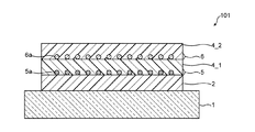
図5は、実施の形態2に係る光素子の断面を模式的に示す図である。
同図には、一例として、実施の形態2に係る光素子101の積層構造の一部が図示されている。
具体的には、第1工程によって形成した樹脂層2上に、金属微粒子5aが分散した分散液(ナノコロイド溶液)をスピンコート法によって塗布する。
具体的には、先ず、第2工程において作製された、金属微粒子層5が形成された積層構造上に、HMDSを公知のスピンコート法によって塗布し、自然乾燥させる。その後、上記第1工程と同様に、上記含フッ素環状重合体溶液を、公知のスピンコート法により、金属微粒子層5が形成された樹脂層2上に塗布する。
具体的には、第3工程によって形成した樹脂層4_1上に、金属微粒子6aが分散した分散液(ナノコロイド溶液)をスピンコート法によって塗布する。
具体的には、先ず、第4工程において作製された、金属微粒子層6が形成された積層構造上に、HMDSを公知のスピンコート法によって塗布し、自然乾燥させる。その後、上記第1工程と同様に、上記含フッ素環状重合体溶液を、公知のスピンコート法により、金属微粒子層6が形成された樹脂層4_1上に塗布する。
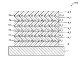
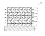
同図に示される光素子101Aは、金属微粒子層5と金属微粒子層6とが交互に複数積層された構造を有し、光素子101Aと同様に、2種類の金属微粒子5a,6bに基づく局在表面プラズモン共鳴による光吸収に基づく非線形光学効果を発現する。
Claims (8)
- 透光性を有する基板と、
前記基板の上に形成され、透光性を有する樹脂から成る複数の樹脂層と、
少なくとも1つの前記樹脂層間に形成され、少なくとも2種類の金属微粒子から成る金属微粒子層とを有する
光素子。 - 請求項1に記載の光素子において、
前記金属微粒子層における前記金属微粒子の密度は、前記金属微粒子の種類毎に異なる
ことを特徴とする光素子。 - 請求項1または2に記載の光素子において、
前記金属微粒子層は、金、銀、および銅のうち少なくとも2つの金属微粒子を含む
ことを特徴とする光素子。 - 透過性を有する基板と、
前記基板の上に形成され、透過性を有する樹脂から構成された複数の樹脂層と、
前記樹脂層の間に夫々形成された複数の金属微粒子層とを有し、
前記複数の金属微粒子層は、第1金属微粒子から構成された第1金属微粒子層と、前記第1金属微粒子とは異なる第2金属微粒子から構成された第2金属微粒子層と、を少なくとも含む
光素子。 - 請求項4に記載の光素子において、
前記第1金属微粒子層の数と前記第2金属微粒子層の数とが相違する
ことを特徴とする光素子。 - 請求項4または5に記載の光素子において、
前記第1金属微粒子は、金、銀、および銅のうち何れか一つの金属材料から成り、
前記第2金属微粒子は、金、銀、および銅のうち前記第1金属微粒子と異なる金属材料から成る
ことを特徴とする光素子。 - 透光性を有する樹脂から構成された樹脂層を形成する第1工程と、
少なくも2種類の金属微粒子が分散した分散液を前記樹脂層上に塗布して、前記樹脂層上に前記金属微粒子を配置する第2工程と、
透光性を有する樹脂を前記金属微粒子が配置された前記樹脂層上に塗布することにより、新たな樹脂層を形成する第3工程とを含む
光素子の製造方法。 - 透光性を有する樹脂から構成された樹脂層を形成する第1工程と、
金属微粒子が分散した分散液を前記樹脂層上に塗布して、前記樹脂層上に金属微粒子を配置する第2工程と、
透光性を有する樹脂を前記金属微粒子が配置された前記樹脂層上に塗布することにより、新たな樹脂層を形成する第3工程とを含み、
前記第2工程と前記第3工程とを繰り返し、前記金属微粒子から成る金属微粒子層を複数形成し、
n(nは2以上の整数)回の前記第2工程のうちm(mは1≦m<nの整数)回の前記第2工程は、第1金属微粒子が分散した分散液を前記樹脂層上に塗布することにより、前記樹脂層上に前記第1金属微粒子から成る第1金属微粒子層を形成する工程であり、残りの(n−m)回の前記第2工程のうち少なくとも1回の工程は、第2金属微粒子が分散した分散液を前記樹脂層上に塗布することにより、前記樹脂層上に前記第2金属微粒子から成る第2金属微粒子層を形成する工程である
光素子の製造方法。
Priority Applications (1)
| Application Number | Priority Date | Filing Date | Title |
|---|---|---|---|
| JP2016095866A JP2017203893A (ja) | 2016-05-12 | 2016-05-12 | 光素子および光素子の製造方法 |
Applications Claiming Priority (1)
| Application Number | Priority Date | Filing Date | Title |
|---|---|---|---|
| JP2016095866A JP2017203893A (ja) | 2016-05-12 | 2016-05-12 | 光素子および光素子の製造方法 |
Publications (1)
| Publication Number | Publication Date |
|---|---|
| JP2017203893A true JP2017203893A (ja) | 2017-11-16 |
Family
ID=60322324
Family Applications (1)
| Application Number | Title | Priority Date | Filing Date |
|---|---|---|---|
| JP2016095866A Pending JP2017203893A (ja) | 2016-05-12 | 2016-05-12 | 光素子および光素子の製造方法 |
Country Status (1)
| Country | Link |
|---|---|
| JP (1) | JP2017203893A (ja) |
Citations (5)
| Publication number | Priority date | Publication date | Assignee | Title |
|---|---|---|---|---|
| JPH03294829A (ja) * | 1990-04-13 | 1991-12-26 | Matsushita Electric Ind Co Ltd | 非線形光学薄膜およびその製造方法 |
| JPH08146477A (ja) * | 1994-11-17 | 1996-06-07 | Matsushita Electric Ind Co Ltd | 非線形光学薄膜およびその製造方法 |
| JP2008232720A (ja) * | 2007-03-19 | 2008-10-02 | Canon Inc | 検出素子、検出素子装置及び検出方法 |
| US20110116168A1 (en) * | 2009-11-13 | 2011-05-19 | Nikoobakht Babak | Nanoengineered devices based on electro-optical modulation of the electrical and optical properties of plasmonic nanoparticles |
| US20150116856A1 (en) * | 2013-10-31 | 2015-04-30 | Korea Institute Of Science And Technology | Plasmonic nano-color coating layer and method for fabricating the same |
-
2016
- 2016-05-12 JP JP2016095866A patent/JP2017203893A/ja active Pending
Patent Citations (5)
| Publication number | Priority date | Publication date | Assignee | Title |
|---|---|---|---|---|
| JPH03294829A (ja) * | 1990-04-13 | 1991-12-26 | Matsushita Electric Ind Co Ltd | 非線形光学薄膜およびその製造方法 |
| JPH08146477A (ja) * | 1994-11-17 | 1996-06-07 | Matsushita Electric Ind Co Ltd | 非線形光学薄膜およびその製造方法 |
| JP2008232720A (ja) * | 2007-03-19 | 2008-10-02 | Canon Inc | 検出素子、検出素子装置及び検出方法 |
| US20110116168A1 (en) * | 2009-11-13 | 2011-05-19 | Nikoobakht Babak | Nanoengineered devices based on electro-optical modulation of the electrical and optical properties of plasmonic nanoparticles |
| US20150116856A1 (en) * | 2013-10-31 | 2015-04-30 | Korea Institute Of Science And Technology | Plasmonic nano-color coating layer and method for fabricating the same |
Similar Documents
| Publication | Publication Date | Title |
|---|---|---|
| Bilal et al. | Elliptical metallic rings-shaped fractal metamaterial absorber in the visible regime | |
| Yu et al. | Structural coloring of glass using dewetted nanoparticles and ultrathin films of metals | |
| Baudrion et al. | Reversible strong coupling in silver nanoparticle arrays using photochromic molecules | |
| Roberts et al. | Subwavelength plasmonic color printing protected for ambient use | |
| Hiller et al. | Reversibly erasable nanoporous anti-reflection coatings from polyelectrolyte multilayers | |
| Lee et al. | Active control of all-fibre graphene devices with electrical gating | |
| Ji et al. | Broadband absorption engineering of hyperbolic metafilm patterns | |
| Kang et al. | Broad-wavelength-range chemically tunable block-copolymer photonic gels | |
| Lee et al. | Tunable metasurfaces for visible and SWIR applications | |
| Caligiuri et al. | Resonant gain singularities in 1D and 3D metal/dielectric multilayered nanostructures | |
| Capretti et al. | Integrating quantum dots and dielectric Mie resonators: a hierarchical metamaterial inheriting the best of both | |
| Choi et al. | Advances in femtosecond laser processing of optical material for device applications | |
| Masharin et al. | Giant ultrafast all-optical modulation based on exceptional points in exciton–polariton perovskite metasurfaces | |
| Lu et al. | Chip-integrated ultrawide-band all-optical logic comparator in plasmonic circuits | |
| Gu et al. | Blue shift of spontaneous emission in hyperbolic metamaterial | |
| Jiang et al. | Colloidal self-assembly based ultrathin metasurface for perfect absorption across the entire visible spectrum | |
| Jin et al. | Inkjet-printed optical interference filters | |
| Galinski et al. | Light manipulation in metallic nanowire networks with functional connectivity | |
| Pianelli et al. | Si-CMOS compatible epsilon-near-zero metamaterial for two-color ultrafast all-optical switching | |
| Khudiyev et al. | Structural coloring in large scale core–shell nanowires | |
| Castillo et al. | Tunable narrowband excitonic Optical Tamm states enabled by a metal-free all-organic structure | |
| Liu et al. | The coupling effects of surface plasmon polaritons and magnetic dipole resonances in metamaterials | |
| Abdel-Galil et al. | Subwavelength focusing in the infrared range using different metasurfaces | |
| Dhuey et al. | Three-dimensional woodpile photonic crystals for visible light applications | |
| Mahros et al. | Investigating the fabrication imperfections of plasmonic nanohole arrays and its effect on the optical transmission spectra |
Legal Events
| Date | Code | Title | Description |
|---|---|---|---|
| A621 | Written request for application examination |
Free format text: JAPANESE INTERMEDIATE CODE: A621 Effective date: 20180625 |
|
| A977 | Report on retrieval |
Free format text: JAPANESE INTERMEDIATE CODE: A971007 Effective date: 20190313 |
|
| A131 | Notification of reasons for refusal |
Free format text: JAPANESE INTERMEDIATE CODE: A131 Effective date: 20190409 |
|
| A521 | Request for written amendment filed |
Free format text: JAPANESE INTERMEDIATE CODE: A523 Effective date: 20190530 |
|
| A131 | Notification of reasons for refusal |
Free format text: JAPANESE INTERMEDIATE CODE: A131 Effective date: 20191015 |
|
| A02 | Decision of refusal |
Free format text: JAPANESE INTERMEDIATE CODE: A02 Effective date: 20200507 |