JP2017510060A - Silicon-on-insulator (SOI) substrate manufacturing method and SOI substrate - Google Patents
Silicon-on-insulator (SOI) substrate manufacturing method and SOI substrate Download PDFInfo
- Publication number
- JP2017510060A JP2017510060A JP2016547879A JP2016547879A JP2017510060A JP 2017510060 A JP2017510060 A JP 2017510060A JP 2016547879 A JP2016547879 A JP 2016547879A JP 2016547879 A JP2016547879 A JP 2016547879A JP 2017510060 A JP2017510060 A JP 2017510060A
- Authority
- JP
- Japan
- Prior art keywords
- patterned
- silicon substrate
- layer
- substrate
- oxide layer
- Prior art date
- Legal status (The legal status is an assumption and is not a legal conclusion. Google has not performed a legal analysis and makes no representation as to the accuracy of the status listed.)
- Granted
Links
Images






Classifications
-
- H—ELECTRICITY
- H10—SEMICONDUCTOR DEVICES; ELECTRIC SOLID-STATE DEVICES NOT OTHERWISE PROVIDED FOR
- H10W—GENERIC PACKAGES, INTERCONNECTIONS, CONNECTORS OR OTHER CONSTRUCTIONAL DETAILS OF DEVICES COVERED BY CLASS H10
- H10W10/00—Isolation regions in semiconductor bodies between components of integrated devices
- H10W10/01—Manufacture or treatment
- H10W10/011—Manufacture or treatment of isolation regions comprising dielectric materials
-
- H—ELECTRICITY
- H10—SEMICONDUCTOR DEVICES; ELECTRIC SOLID-STATE DEVICES NOT OTHERWISE PROVIDED FOR
- H10P—GENERIC PROCESSES OR APPARATUS FOR THE MANUFACTURE OR TREATMENT OF DEVICES COVERED BY CLASS H10
- H10P90/00—Preparation of wafers not covered by a single main group of this subclass, e.g. wafer reinforcement
- H10P90/19—Preparing inhomogeneous wafers
- H10P90/1904—Preparing vertically inhomogeneous wafers
- H10P90/1906—Preparing SOI wafers
- H10P90/1914—Preparing SOI wafers using bonding
- H10P90/1916—Preparing SOI wafers using bonding with separation or delamination along an ion implanted layer, e.g. Smart-cut
-
- H—ELECTRICITY
- H10—SEMICONDUCTOR DEVICES; ELECTRIC SOLID-STATE DEVICES NOT OTHERWISE PROVIDED FOR
- H10F—INORGANIC SEMICONDUCTOR DEVICES SENSITIVE TO INFRARED RADIATION, LIGHT, ELECTROMAGNETIC RADIATION OF SHORTER WAVELENGTH OR CORPUSCULAR RADIATION
- H10F71/00—Manufacture or treatment of devices covered by this subclass
- H10F71/127—The active layers comprising only Group III-V materials, e.g. GaAs or InP
- H10F71/1278—The active layers comprising only Group III-V materials, e.g. GaAs or InP comprising nitrides, e.g. GaN
-
- H—ELECTRICITY
- H10—SEMICONDUCTOR DEVICES; ELECTRIC SOLID-STATE DEVICES NOT OTHERWISE PROVIDED FOR
- H10H—INORGANIC LIGHT-EMITTING SEMICONDUCTOR DEVICES HAVING POTENTIAL BARRIERS
- H10H20/00—Individual inorganic light-emitting semiconductor devices having potential barriers, e.g. light-emitting diodes [LED]
- H10H20/01—Manufacture or treatment
- H10H20/011—Manufacture or treatment of bodies, e.g. forming semiconductor layers
- H10H20/018—Bonding of wafers
-
- H—ELECTRICITY
- H10—SEMICONDUCTOR DEVICES; ELECTRIC SOLID-STATE DEVICES NOT OTHERWISE PROVIDED FOR
- H10P—GENERIC PROCESSES OR APPARATUS FOR THE MANUFACTURE OR TREATMENT OF DEVICES COVERED BY CLASS H10
- H10P14/00—Formation of materials, e.g. in the shape of layers or pillars
- H10P14/20—Formation of materials, e.g. in the shape of layers or pillars of semiconductor materials
- H10P14/34—Deposited materials, e.g. layers
- H10P14/3402—Deposited materials, e.g. layers characterised by the chemical composition
- H10P14/3414—Deposited materials, e.g. layers characterised by the chemical composition being group IIIA-VIA materials
- H10P14/3416—Nitrides
-
- H—ELECTRICITY
- H10—SEMICONDUCTOR DEVICES; ELECTRIC SOLID-STATE DEVICES NOT OTHERWISE PROVIDED FOR
- H10P—GENERIC PROCESSES OR APPARATUS FOR THE MANUFACTURE OR TREATMENT OF DEVICES COVERED BY CLASS H10
- H10P14/00—Formation of materials, e.g. in the shape of layers or pillars
- H10P14/20—Formation of materials, e.g. in the shape of layers or pillars of semiconductor materials
- H10P14/34—Deposited materials, e.g. layers
- H10P14/3402—Deposited materials, e.g. layers characterised by the chemical composition
- H10P14/3414—Deposited materials, e.g. layers characterised by the chemical composition being group IIIA-VIA materials
- H10P14/3418—Phosphides
-
- H—ELECTRICITY
- H10—SEMICONDUCTOR DEVICES; ELECTRIC SOLID-STATE DEVICES NOT OTHERWISE PROVIDED FOR
- H10P—GENERIC PROCESSES OR APPARATUS FOR THE MANUFACTURE OR TREATMENT OF DEVICES COVERED BY CLASS H10
- H10P14/00—Formation of materials, e.g. in the shape of layers or pillars
- H10P14/20—Formation of materials, e.g. in the shape of layers or pillars of semiconductor materials
- H10P14/34—Deposited materials, e.g. layers
- H10P14/3402—Deposited materials, e.g. layers characterised by the chemical composition
- H10P14/3414—Deposited materials, e.g. layers characterised by the chemical composition being group IIIA-VIA materials
- H10P14/3421—Arsenides
-
- H—ELECTRICITY
- H10—SEMICONDUCTOR DEVICES; ELECTRIC SOLID-STATE DEVICES NOT OTHERWISE PROVIDED FOR
- H10P—GENERIC PROCESSES OR APPARATUS FOR THE MANUFACTURE OR TREATMENT OF DEVICES COVERED BY CLASS H10
- H10P14/00—Formation of materials, e.g. in the shape of layers or pillars
- H10P14/20—Formation of materials, e.g. in the shape of layers or pillars of semiconductor materials
- H10P14/34—Deposited materials, e.g. layers
- H10P14/3402—Deposited materials, e.g. layers characterised by the chemical composition
- H10P14/3414—Deposited materials, e.g. layers characterised by the chemical composition being group IIIA-VIA materials
- H10P14/3422—Antimonides
-
- H—ELECTRICITY
- H10—SEMICONDUCTOR DEVICES; ELECTRIC SOLID-STATE DEVICES NOT OTHERWISE PROVIDED FOR
- H10P—GENERIC PROCESSES OR APPARATUS FOR THE MANUFACTURE OR TREATMENT OF DEVICES COVERED BY CLASS H10
- H10P50/00—Etching of wafers, substrates or parts of devices
- H10P50/73—Etching of wafers, substrates or parts of devices using masks for insulating materials
-
- H—ELECTRICITY
- H10—SEMICONDUCTOR DEVICES; ELECTRIC SOLID-STATE DEVICES NOT OTHERWISE PROVIDED FOR
- H10P—GENERIC PROCESSES OR APPARATUS FOR THE MANUFACTURE OR TREATMENT OF DEVICES COVERED BY CLASS H10
- H10P90/00—Preparation of wafers not covered by a single main group of this subclass, e.g. wafer reinforcement
- H10P90/19—Preparing inhomogeneous wafers
- H10P90/1904—Preparing vertically inhomogeneous wafers
- H10P90/1906—Preparing SOI wafers
- H10P90/1912—Preparing SOI wafers using selective deposition, e.g. epitaxial lateral overgrowth [ELO] or selective deposition of single crystal silicon
-
- H—ELECTRICITY
- H10—SEMICONDUCTOR DEVICES; ELECTRIC SOLID-STATE DEVICES NOT OTHERWISE PROVIDED FOR
- H10W—GENERIC PACKAGES, INTERCONNECTIONS, CONNECTORS OR OTHER CONSTRUCTIONAL DETAILS OF DEVICES COVERED BY CLASS H10
- H10W10/00—Isolation regions in semiconductor bodies between components of integrated devices
- H10W10/10—Isolation regions comprising dielectric materials
-
- H—ELECTRICITY
- H10—SEMICONDUCTOR DEVICES; ELECTRIC SOLID-STATE DEVICES NOT OTHERWISE PROVIDED FOR
- H10W—GENERIC PACKAGES, INTERCONNECTIONS, CONNECTORS OR OTHER CONSTRUCTIONAL DETAILS OF DEVICES COVERED BY CLASS H10
- H10W10/00—Isolation regions in semiconductor bodies between components of integrated devices
- H10W10/10—Isolation regions comprising dielectric materials
- H10W10/181—Semiconductor-on-insulator [SOI] isolation regions, e.g. buried oxide regions of SOI wafers
Landscapes
- Recrystallisation Techniques (AREA)
- Physical Vapour Deposition (AREA)
- Chemical Vapour Deposition (AREA)
Abstract
SOI基板製造方法及びSOI基板が提供される。SOI基板製造方法は、第一のシリコン基板(110)の酸化層(120)内にパターン化エッチストップ層(130)を形成するステップと、パターン化エッチストップ層(130)を有する第一のシリコン基板(110)の表面を第二のシリコン基板(210)の表面に結合させるステップと、第一のシリコン基板(110)の一部を剥離させてパターン化シリコン・オン・インシュレータSOI基板(300)を形成するステップとを含む。ヘテロエピタキシャル層をSOI基板のシリコン層上に成長させる際に、シリコン層とヘテロエピタキシャル層との間に格子不整合及び熱的不整合が生じるという従来技術の問題が解決される。貫通転位を有さないヘテロエピタキシャル層をSOI基板のシリコン層上に形成することができ、シリコン基板とヘテロエピタキシャル層との間の格子不整合の割合が大幅に減り、光電デバイスの使用性能及び信頼性が改善される。An SOI substrate manufacturing method and an SOI substrate are provided. An SOI substrate manufacturing method includes forming a patterned etch stop layer (130) in an oxide layer (120) of a first silicon substrate (110), and a first silicon having a patterned etch stop layer (130). Bonding the surface of the substrate (110) to the surface of the second silicon substrate (210) and peeling off a portion of the first silicon substrate (110) to form a patterned silicon-on-insulator SOI substrate (300). Forming a step. When the heteroepitaxial layer is grown on the silicon layer of the SOI substrate, the problem of the prior art that a lattice mismatch and a thermal mismatch occur between the silicon layer and the heteroepitaxial layer is solved. A heteroepitaxial layer having no threading dislocation can be formed on the silicon layer of the SOI substrate, and the rate of lattice mismatch between the silicon substrate and the heteroepitaxial layer is greatly reduced, and the usage performance and reliability of the photoelectric device are reduced. Improved.
Description
本発明の実施形態は半導体デバイス技術に係り、特にSOI基板製造方法及びSOI基板に関する。 Embodiments described herein relate generally to semiconductor device technology, and more particularly, to an SOI substrate manufacturing method and an SOI substrate.
半導体集積回路の小型化及び多様化に伴い、デバイスのフィーチャサイズが減少し、デバイスの集積が改善されている一方で、信号遅延や相互接続クロストーク等の問題が生じている。電気的相互接続誘電体の共通使用によって生じる高電力消費及びエネルギーの無駄のため、デバイスに対する高性能且つ低コストという半導体業界の要求は既に満たすことができないものになっている。他方、光学的相互接続は上記問題を効果的に解決して、従来の集積回路に多数の新たな機能をもたらすことができるので、光電デバイスが、半導体デバイスの高集積開発のための主な指針となっている。 With the miniaturization and diversification of semiconductor integrated circuits, device feature sizes have decreased and device integration has improved, while problems such as signal delay and interconnect crosstalk have arisen. The high power consumption and energy waste caused by the common use of electrical interconnect dielectrics has already made it impossible for the semiconductor industry to meet the high performance and low cost requirements for devices. On the other hand, optical interconnects can effectively solve the above problems and bring many new functions to conventional integrated circuits, so that photoelectric devices are the main guideline for highly integrated development of semiconductor devices. It has become.
現状で一般的に使われているシリコン・オン・インシュレータ(Silicon On Insulator,SOI)基板は、頂部層シリコン基板と底部層シリコン基板との間に埋め込まれた酸化層を導入することによって、得られる。具体的には、半導体薄膜が絶縁体上に形成されて、SOI基板は、バルクシリコン基板とは比較にならない利点を有する。例えば、SOI基板は、集積回路の部品間に誘電体分離を実現して、バルクシリコンの相補型金属酸化膜半導体(Complementary Metal Oxide Semiconductor,CMOS)回路における寄生ラッチアップ効果を排除することができる。SOI基板を用いて製造された集積回路は、低寄生キャパシタンス、高集積密度、高速性、簡易技術、低短絡効果等の利点を更に有し、特に、低電圧及び低電力消費回路に適用可能である。従って、SOI基板は、ディープサブミクロン、低電圧及び低電力消費集積回路の主流技術となる可能性がある。しかしながら、SOI基板を用いた光電デバイスや光導波デバイスの製造プロセスにおいては、ヘテロ接合をエピタキシャル成長させる必要がある。例えば、III‐V族化合物を、SOI基板のシリコン層上にエピタキシャル成長させると、良好な光電性能を有する基板物質が得られ、光電デバイスの基板物質とするのに適している。 A silicon on insulator (SOI) substrate that is generally used at present is obtained by introducing an oxide layer embedded between a top layer silicon substrate and a bottom layer silicon substrate. . Specifically, a semiconductor thin film is formed on an insulator, and an SOI substrate has an advantage that cannot be compared with a bulk silicon substrate. For example, an SOI substrate can provide dielectric isolation between components of an integrated circuit to eliminate parasitic latch-up effects in a bulk silicon complementary metal oxide semiconductor (CMOS) circuit. An integrated circuit manufactured using an SOI substrate further has advantages such as low parasitic capacitance, high integration density, high speed, simple technology, and low short-circuit effect, and is particularly applicable to low voltage and low power consumption circuits. is there. Thus, SOI substrates can become the mainstream technology for deep sub-micron, low voltage and low power consumption integrated circuits. However, in the manufacturing process of the photoelectric device and the optical waveguide device using the SOI substrate, it is necessary to epitaxially grow the heterojunction. For example, when a group III-V compound is epitaxially grown on a silicon layer of an SOI substrate, a substrate material having good photoelectric performance is obtained, which is suitable as a substrate material for a photoelectric device.
従来技術では、ヘテロエピタキシャル層をSOI基板のシリコン層上に成長させる際に、シリコン層とヘテロエピタキシャル層との間で格子不整合及び熱的不整合が生じるので、高密度の貫通転位の問題が基板に生じて、光電デバイスの使用性能及び信頼性を低下させる。 In the prior art, when the heteroepitaxial layer is grown on the silicon layer of the SOI substrate, lattice mismatching and thermal mismatching occur between the silicon layer and the heteroepitaxial layer. It occurs in the substrate and reduces the usage performance and reliability of the photoelectric device.
本発明の実施形態は、ヘテロエピタキシャル層をSOI基板のシリコン層上に成長させる際に、シリコン層とヘテロエピタキシャル層との間で格子不整合及び熱的不整合が生じて、高密度の貫通転位をもたらすという従来技術の問題を解決するために、SOI基板製造方法及びSOI基板を提供する。 In embodiments of the present invention, when a heteroepitaxial layer is grown on a silicon layer of an SOI substrate, lattice mismatches and thermal mismatches occur between the silicon layer and the heteroepitaxial layer, resulting in a high density of threading dislocations. In order to solve the problems of the prior art that cause the problem, an SOI substrate manufacturing method and an SOI substrate are provided.
第一の態様によると、本発明の一実施形態は、
第一のシリコン基板の酸化層内にパターン化エッチストップ層を形成するステップと、
パターン化エッチストップ層を有する第一のシリコン基板の表面を第二のシリコン基板の表面と結合させて、第一のシリコン基板の一部を剥離させて、パターン化シリコン・オン・インシュレータSOI基板を形成するステップと、を含むSOI基板製造方法を提供する。
According to a first aspect, an embodiment of the present invention is
Forming a patterned etch stop layer in the oxide layer of the first silicon substrate;
Bonding the surface of the first silicon substrate with the patterned etch stop layer with the surface of the second silicon substrate and peeling off a portion of the first silicon substrate to form a patterned silicon-on-insulator SOI substrate. And forming an SOI substrate.
第一の態様の第一の可能な実施方式では、第一のシリコン基板の酸化層内にパターン化エッチストップ層を形成するステップは、
第一のシリコン基板上に第一の酸化層を形成するステップと、
第一のシリコン基板の第一の酸化層上にパターン化エッチストップ層を形成するステップと、を含む。
In a first possible implementation of the first aspect, the step of forming a patterned etch stop layer in the oxide layer of the first silicon substrate comprises:
Forming a first oxide layer on a first silicon substrate;
Forming a patterned etch stop layer on the first oxide layer of the first silicon substrate.
第一の態様の第一の可能な実施方式に従う第二の可能な実施方式では、第一のシリコン基板の第一の酸化層上にパターン化エッチストップ層を形成するステップは、
第一のシリコン基板の第一の酸化層上にエッチストップ層を形成するステップと、
エッチストップ層上にパターン化マスクを形成して、エッチングによってパターン化エッチストップ層を得るステップと、を含み、パターン化マスクは、極紫外線リソグラフィEUV法を用いて得られるパターン化フォトレジストを含む。
In a second possible implementation according to the first possible implementation of the first aspect, the step of forming a patterned etch stop layer on the first oxide layer of the first silicon substrate comprises:
Forming an etch stop layer on the first oxide layer of the first silicon substrate;
Forming a patterned mask on the etch stop layer to obtain a patterned etch stop layer by etching, the patterned mask comprising a patterned photoresist obtained using an extreme ultraviolet lithography EUV method.
第一の態様の第一の可能な実施方式に従う第三の可能な実施方式では、第一のシリコン基板の第一の酸化層上にパターン化エッチストップ層を形成するステップは、
第一のシリコン基板の第一の酸化層上にエッチストップ層を形成するステップと、
エッチストップ層上にパターン化マスクを形成して、エッチングによってパターン化エッチストップ層を得るステップと、を含み、パターン化マスクは多孔質アルミナフィルムを含む。
In a third possible implementation according to the first possible implementation of the first aspect, the step of forming a patterned etch stop layer on the first oxide layer of the first silicon substrate comprises:
Forming an etch stop layer on the first oxide layer of the first silicon substrate;
Forming a patterned mask on the etch stop layer to obtain a patterned etch stop layer by etching, wherein the patterned mask comprises a porous alumina film.
第一の態様の第一から第三の可能な実施方式のうちいずれか一つに従う第四の可能な実施方式では、第一のシリコン基板の第一の酸化層上にパターン化エッチストップ層を形成するステップの後に、本方法は、
パターン化エッチストップ層上に第二の酸化層を成長させて、第二の酸化層に対して平坦化処理及び化学的表面処理を行うステップを更に含む。
In a fourth possible implementation manner according to any one of the first to third possible implementation manners of the first aspect, a patterned etch stop layer is provided on the first oxide layer of the first silicon substrate. After the forming step, the method
The method further includes growing a second oxide layer on the patterned etch stop layer and subjecting the second oxide layer to planarization and chemical surface treatment.
第一の態様の第一から第四の可能な実施方式のうちいずれか一つに従う第五の可能な実施方式では、第一のシリコン基板の第一の酸化層上にパターン化エッチストップ層を形成するステップの前に、本方法は、
第一のシリコン基板に対してイオン注入を行い、第一のシリコン基板のシリコン層内に欠陥層を形成するステップを更に含み、第一のシリコン基板の一部を剥離させることが、第一のシリコン基板内の欠陥層と、欠陥層上のシリコン層とを剥離させることを含み、
パターン化エッチストップ層を有する第一のシリコン基板の表面を第二のシリコン基板の表面と結合させて、第一のシリコン基板の一部を剥離させて、パターン化シリコン・オン・インシュレータSOI基板を形成するステップの後に、本方法は、
低温アニーリング処理を行い、第一のシリコン基板及び第二のシリコン基板の隣接した表面を強固に結合させるステップと、
パターン化SOI基板に対して表面研磨処理を行うステップを更に含む。
In a fifth possible implementation according to any one of the first to fourth possible implementations of the first aspect, a patterned etch stop layer is provided on the first oxide layer of the first silicon substrate. Prior to the forming step, the method
The method further includes the step of ion-implanting the first silicon substrate to form a defect layer in the silicon layer of the first silicon substrate, and peeling a part of the first silicon substrate includes the steps of: Peeling off the defective layer in the silicon substrate and the silicon layer on the defective layer,
Bonding the surface of the first silicon substrate with the patterned etch stop layer with the surface of the second silicon substrate and peeling off a portion of the first silicon substrate to form a patterned silicon-on-insulator SOI substrate. After the forming step, the method
Performing a low temperature annealing process to firmly bond adjacent surfaces of the first silicon substrate and the second silicon substrate;
The method further includes performing a surface polishing process on the patterned SOI substrate.
第一の態様及びその第一の態様の第一から第五の可能な実施方式のうちいずれか一つに従う第六の可能な実施方式では、パターン化エッチストップ層の物質は、酸化層に対してエッチング選択性を有する物質である。 In a sixth possible implementation manner according to the first aspect and any one of the first to fifth possible implementation manners of the first aspect, the material of the patterned etch stop layer is relative to the oxide layer. And a material having etching selectivity.
第一の態様及びその第一の態様の第一から第六の可能な実施方式のうちいずれか一つに従う第七の可能な実施方式では、パターン化エッチストップ層のパターンサイズは20nm未満であり、パターン化エッチストップ層の厚さは50nm未満である。 In a seventh possible implementation manner according to the first aspect and any one of the first to sixth possible implementation manners of the first aspect, the pattern size of the patterned etch stop layer is less than 20 nm. The thickness of the patterned etch stop layer is less than 50 nm.
第一の態様及びその第一の態様の第一から第七の可能な実施方式のうちいずれか一つに従う第八の可能な実施方式では、本方法は、
パターン化SOI基板上にパターン化マスクを形成して、デバイス形成領域を露出させるステップと、
パターン化SOI基板上のデバイス形成領域をエッチングして、第二のシリコン基板上にパターン化酸化層を得るステップと、
デバイス形成領域内にIII‐V族化合物をエピタキシャル成長させて、デバイス構造を形成するステップと、を更に含む。
In an eighth possible implementation manner according to any one of the first aspect and the first to seventh possible implementation manners of the first aspect, the method comprises:
Forming a patterned mask on a patterned SOI substrate to expose a device formation region;
Etching a device formation region on the patterned SOI substrate to obtain a patterned oxide layer on the second silicon substrate;
And epitaxially growing a III-V compound in the device formation region to form a device structure.
第一の態様の第八の可能な実施方式に従う第九の可能な実施方式では、パターン化SOI基板上のデバイス形成領域をエッチングして、第二のシリコン基板上にパターン化酸化層を得るステップは、
パターン化SOI基板上のデバイス形成領域内の第一のシリコン基板のシリコン層と、第一の酸化層と、第二の酸化層の一部とをエッチングして、第二のシリコン基板上のパターン化酸化層及びパターン化エッチストップ層を得るステップであって、パターン化酸化層がパターン化エッチストップ層の下に存在する、ステップと、
パターン化SOI基板上のデバイス形成領域内のパターン化エッチストップ層を除去して、第二のシリコン基板上にパターン化酸化層を得るステップと、を含む。
In a ninth possible implementation manner in accordance with the eighth possible implementation manner of the first aspect, the step of etching the device forming region on the patterned SOI substrate to obtain a patterned oxide layer on the second silicon substrate Is
A pattern on the second silicon substrate is etched by etching the silicon layer of the first silicon substrate, the first oxide layer, and a part of the second oxide layer in the device formation region on the patterned SOI substrate. Obtaining a patterned oxide layer and a patterned etch stop layer, wherein the patterned oxide layer is present under the patterned etch stop layer;
Removing the patterned etch stop layer in the device formation region on the patterned SOI substrate to obtain a patterned oxide layer on the second silicon substrate.
第一の態様の第八又は第九の可能な実施方式に従う第十の可能な実施方式では、デバイス形成領域内にIII‐V族化合物をエピタキシャル成長させて、デバイス基板を形成するステップは、
パターン化酸化層が既に得られている第二のシリコン基板上に第三の酸化層を成長させるステップであって、第三の酸化層が前記デバイス形成領域外に成長する、ステップと、
第三の酸化層が既に成長している第二のシリコン基板のパターン化酸化層上にIII‐V族化合物をエピタキシャル成長させて、デバイス構造を形成するステップと、を含み、エピタキシャル成長させたIII‐V族化合物は、第二のシリコン基板のパターン化酸化層のパターン内において第二のシリコン基板に接続される。
In a tenth possible implementation manner according to the eighth or ninth possible implementation manner of the first aspect, the step of epitaxially growing a group III-V compound in the device formation region to form a device substrate comprises:
Growing a third oxide layer on a second silicon substrate from which a patterned oxide layer has already been obtained, wherein the third oxide layer is grown outside the device formation region;
Epitaxially growing a III-V compound on a patterned oxide layer of a second silicon substrate on which a third oxide layer has already been grown to form a device structure, and epitaxially growing the III-V The group compound is connected to the second silicon substrate in the pattern of the patterned oxide layer of the second silicon substrate.
第一の態様の第八から第十の可能な実施方式のうちいずれか一つに従う第十一の可能な実施方式では、III‐V族化合物は、リン化アルミニウムAlP、リン化ガリウムGaP、リン化インジウムInP、ヒ化アルミニウムAlAs、ヒ化ガリウムGaAs、ヒ化インジウムInAs、アンチモン化アルミニウムAlSb、アンチモン化ガリウムGaSb、アンチモン化インジウムInSb、窒化アルミニウムAlN、窒化ガリウムGaN、窒化インジウムInN、又は、これらの三元化合物及び四元化合物を含む。 In an eleventh possible implementation manner according to any one of the eighth to tenth possible implementation manners of the first aspect, the group III-V compound comprises aluminum phosphide AlP, gallium phosphide GaP, phosphorous InP InP, aluminum arsenide AlAs, gallium arsenide GaAs, indium arsenide InAs, aluminum antimonide AlSb, gallium antimonide GaSb, indium antimonide InSb, aluminum nitride AlN, gallium nitride GaN, indium nitride InN, or these Includes ternary and quaternary compounds.
第一の態様の第八から第十一の可能な実施方式のうちいずれか一つに従う第十二の可能な実施方式では、デバイス形成領域内にIII‐V族化合物をエピタキシャル成長させて、デバイス基板を形成するステップは、
分子線エピタキシMBE法、化学気相堆積CVD法、原子層堆積ALD法、又はこれらの変形法を用いて、デバイス形成領域内にIII‐V族化合物を成長させて、デバイス基板を形成するステップを含む。
In a twelfth possible implementation manner according to any one of the eighth to eleventh possible implementation manners of the first aspect, a group III-V compound is epitaxially grown in the device formation region to obtain a device substrate. The step of forming
Using the molecular beam epitaxy MBE method, the chemical vapor deposition CVD method, the atomic layer deposition ALD method, or a modified method thereof, growing a group III-V compound in the device formation region to form a device substrate Including.
第一の態様の第八から第十二の可能な実施方式のうちいずれか一つに従う第十三の可能な実施方式では、本方法は、
デバイス基板が既に形成されているパターン化SOI基板に対してアニーリング処理を行い、デバイス形成領域内におけるIII‐V族化合物のエピタキシャル・ラテラル・オーバーグロースELOによって生じる欠陥を減らすステップを更に含む。
In a thirteenth possible implementation manner according to any one of the eighth to twelfth possible implementation manners of the first aspect, the method comprises:
The method further includes annealing the patterned SOI substrate on which the device substrate has already been formed to reduce defects caused by the III-V compound epitaxial lateral overgrowth ELO in the device formation region.
第一の態様の第八から第十三の可能な実施方式のうちいずれか一つに従う第十四の可能な実施方式では、本方法は、
デバイス構造内に光電デバイス構造を形成するステップを更に含み、光電デバイス構造が多層構造を有する。
In a fourteenth possible implementation manner according to any one of the eighth to thirteenth possible implementation manners of the first aspect, the method comprises:
The method further includes forming a photoelectric device structure within the device structure, wherein the photoelectric device structure has a multilayer structure.
第二の態様によると、本発明の一実施形態は、上記本発明の実施形態において提供されるSOI基板製造方法を用いて製造されたSOI基板を提供する。 According to a second aspect, an embodiment of the present invention provides an SOI substrate manufactured using the SOI substrate manufacturing method provided in the above embodiment of the present invention.
本実施形態において提供されるSOI基板製造方法及びSOI基板によると、パターン化エッチストップ層を第一のシリコン基板の酸化層内に形成し、パターン化エッチストップ層を有する第一のシリコン基板の表面を第二のシリコン基板のシリコン表面に結合させて、第一のシリコン基板の一部を剥離させて、処理後にパターン化SOI基板を形成するが、これは、ヘテロエピタキシャル層をSOI基板のシリコン層上に成長させる際に、シリコン層とヘテロエピタキシャル層との間に格子不整合及び熱的不整合が生じて、高密度の貫通転位をもたらすという従来技術の問題を解決する。本実施形態において提供されるパターン化SOI基板では、貫通転位を有さないヘテロエピタキシャル層をシリコン基板上に形成することができ、光電デバイスの使用性能及び信頼性が改善される。 According to the SOI substrate manufacturing method and the SOI substrate provided in this embodiment, the patterned etch stop layer is formed in the oxide layer of the first silicon substrate, and the surface of the first silicon substrate having the patterned etch stop layer is formed. Is bonded to the silicon surface of the second silicon substrate, and a part of the first silicon substrate is peeled off to form a patterned SOI substrate after processing, in which the heteroepitaxial layer is transformed into the silicon layer of the SOI substrate. It solves the prior art problem of lattice mismatch and thermal mismatch between the silicon layer and the heteroepitaxial layer when grown on it, resulting in a high density of threading dislocations. In the patterned SOI substrate provided in this embodiment, a heteroepitaxial layer having no threading dislocation can be formed on a silicon substrate, and the use performance and reliability of the photoelectric device are improved.
以下、本発明の実施形態又は従来技術における技術的解決策をより明確に説明するため、本実施形態又は従来技術を説明するのに必要な添付図面について簡単に説明する。以下説明の添付図面が本発明の一部実施形態を示すものであることは明らかであり、当業者は、創作的活動を行わずに、これらの添付図面からなおも他の図面を導き出し得るものである。 Hereinafter, in order to describe the technical solutions in the embodiments of the present invention or the prior art more clearly, the accompanying drawings necessary for describing the embodiments or the prior art will be briefly described. It is obvious that the accompanying drawings described below show some embodiments of the present invention, and those skilled in the art can still derive other drawings from these accompanying drawings without performing creative activities. It is.
以下、本発明の実施形態の目的、技術的解決策及び利点をより明らかにするため、本発明の実施形態の添付図面を参照して、本発明の実施形態の技術的解決策を明確且つ完全に説明する。説明される実施形態が本発明の実施形態の一部であって全部ではないことは明らかである。当業者が創作的活動を行わずに本発明の実施形態に基づいて得る他の全ての実施形態は、本発明の保護範囲内に含まれるものである。 Hereinafter, in order to clarify the objects, technical solutions, and advantages of the embodiments of the present invention, the technical solutions of the embodiments of the present invention will be clearly and completely described with reference to the accompanying drawings of the embodiments of the present invention. Explained. Apparently, the described embodiments are a part rather than all of the embodiments of the present invention. All other embodiments obtained by a person of ordinary skill in the art based on the embodiments of the present invention without performing creative activities shall fall within the protection scope of the present invention.
[実施形態1]
図1は、本発明の実施形態1に係るSOI基板製造方法のフローチャートである。本実施形態の方法は、半導体デバイス基板の製造の場合に適用可能である。本実施形態の方法は以下のステップを含む。
[Embodiment 1]
FIG. 1 is a flowchart of an SOI substrate manufacturing method according to
S110:第一のシリコン基板の酸化層内にパターン化エッチストップ層を形成するステップ S110: forming a patterned etch stop layer in the oxide layer of the first silicon substrate
現状で一般的に用いられているSOI基板の構造では、酸化層は頂部層シリコン基板と底部層シリコン基板との間に導入される。図2に示されるように、図2は、従来技術に係るSOI基板の概略構造図である。従来技術におけるSOI基板の製造は、一般的に、二つのウェーハ基板、具体的にはシリコン基板A及びシリコン基板Bを要する。酸化層をシリコン基板A上に形成して、酸化層を有するシリコン基板Aを反転させて、シリコン基板Bのシリコン表面と結合させる。具体的には、シリコン基板Aの酸化層をシリコン基板Bの表面上のシリコン層と結合させて、酸化層が頂部層シリコン基板と底部層シリコン基板との間に存在している基板構造を形成する。既存のSOI基板は一般的なシリコン基板よりも優れた性能を有するが、ヘテロ接合を既存のSOI基板のシリコン層上にエピタキシャル成長させる際には、エピタキシャル層になおも転移が生じる。従来技術とは異なり、本実施形態では、二つのシリコン基板の間の酸化層内にパターン化されたフィルムが存在している。図3Aに示されるように、図3Aは、図1に示される実施形態に係るSOI基板製造方法における基板構造の概略図である。特定の製造プロセスにおいて、パターン化エッチストップ層130を第一のシリコン基板110の酸化層120内に形成し得て、パターン化エッチストップ層130は酸化層120の中部及び上部に形成される。
In the structure of an SOI substrate generally used at present, an oxide layer is introduced between a top layer silicon substrate and a bottom layer silicon substrate. As shown in FIG. 2, FIG. 2 is a schematic structural diagram of an SOI substrate according to the prior art. The manufacture of SOI substrates in the prior art generally requires two wafer substrates, specifically silicon substrate A and silicon substrate B. An oxide layer is formed on the silicon substrate A, and the silicon substrate A having the oxide layer is inverted and bonded to the silicon surface of the silicon substrate B. Specifically, the oxide layer of the silicon substrate A is combined with the silicon layer on the surface of the silicon substrate B to form a substrate structure in which the oxide layer exists between the top layer silicon substrate and the bottom layer silicon substrate. To do. Existing SOI substrates have better performance than typical silicon substrates, but when a heterojunction is epitaxially grown on a silicon layer of an existing SOI substrate, a transition still occurs in the epitaxial layer. Unlike the prior art, in this embodiment there is a patterned film in the oxide layer between the two silicon substrates. As shown in FIG. 3A, FIG. 3A is a schematic view of the substrate structure in the SOI substrate manufacturing method according to the embodiment shown in FIG. In a particular manufacturing process, a patterned
本実施形態では、パターン化エッチストップ層130のパターンサイズは20nm未満となり得て、パターン化エッチストップ層130の厚さは50nm未満となり得る点に留意されたい。同様に、パターン化エッチストップ層130の上方の酸化層の厚さも50nm未満となり得て、パターン化エッチストップ層130の上方及び下方の酸化層は全体として接続される。
It should be noted that in this embodiment, the pattern size of the patterned
Luryi及びSuhirによって提案されている理論によると、以下の式(1)で示されるように、基板上のエピタキシャル層に垂直な応力場σは、成長方向zにおいて指数関数的に減衰する:
σ ∝ e−πz/(2l) (1)
According to the theory proposed by Luryi and Suhir, the stress field σ normal to the epitaxial layer on the substrate decays exponentially in the growth direction z, as shown in equation (1) below:
σ e e −πz / (2l) (1)
上記式(1)において、2lはパターンの横寸法であり、パターンサイズが減少するにつれて、応力場σが指数関数的に減衰することが分かる。従って、パターンが十分小さい限り、転移が生じるエピタキシャル層の臨界厚さは無限と見なされ、これは、貫通転位を有さないヘテロエピタキシャル層をシリコン基板上に形成できることと同義である。 In the above equation (1), 2l is the lateral dimension of the pattern, and it can be seen that the stress field σ decays exponentially as the pattern size decreases. Therefore, as long as the pattern is sufficiently small, the critical thickness of the epitaxial layer where the transition occurs is considered infinite, which is synonymous with the ability to form a heteroepitaxial layer without threading dislocations on the silicon substrate.
本実施形態で提供されるSOI基板製造方法によると、パターンサイズが極めて小さいパターン化エッチストップ層130を、第一のシリコン基板110の酸化層120内に形成する。本方法を用いて製造されたSOI基板は、シリコンに対して格子不整合を有する物質を成長させるのに適用可能であり、貫通転位を有さないヘテロエピタキシャル層をシリコン基板上に形成することができる。
According to the SOI substrate manufacturing method provided in the present embodiment, the patterned
S120:パターン化エッチストップ層を有する第一のシリコン基板の表面を第二のシリコン基板のシリコン表面と結合させて、第一のシリコン基板の一部を剥離させて、パターン化シリコン・オン・インシュレータSOI基板を形成するステップ S120: The surface of the first silicon substrate having the patterned etch stop layer is bonded to the silicon surface of the second silicon substrate, and a part of the first silicon substrate is peeled off to form a patterned silicon-on-insulator. Forming an SOI substrate;
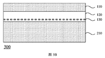
本実施形態では、パターン化エッチストップ層130は、第一のシリコン基板110の酸化層120内に既に形成されていて、第二のシリコン基板210の表面上に薄い酸化層が存在し得て、第二のシリコン基板210の表面上の酸化層は、自然酸化層であるか、又は、熱酸化法を用いて形成され得る。第一のシリコン基板110及び第二のシリコン基板210に対して結合処理を行う際には、第一のシリコン基板110を反転させて、パターン化エッチストップ層130を有する第一のシリコン基板110の表面を第二のシリコン基板210の表面と結合させて、その後、第一のシリコン基板110の一部を剥離させて、酸化層120が第一のシリコン基板110と第二のシリコン基板210との間に存在している基板構造、つまりパターン化SOI基板300を得る。図3Bに示されるように、図3Bは、図1に示される実施形態に係るSOI基板製造方法における基板構造の概略図である。また、パターン化エッチストップ層130は、本実施形態で提供されるパターン化SOI基板300の酸化層120内に存在している。
In this embodiment, the patterned
本実施形態で提供されるSOI基板製造方法によると、パターン化エッチストップ層を第一のシリコン基板の酸化層内に形成して、パターン化エッチストップ層を有する第一のシリコン基板の表面を第二のシリコン基板のシリコン表面と結合させて、第一のシリコン基板の一部を剥離させて、パターン化SOI基板を形成する。本構造は、ヘテロエピタキシャル層をSOI基板のシリコン層上に成長させる際に、シリコン層とヘテロエピタキシャル層との間に生じる格子不整合及び熱的不整合によって、多量の貫通転位がエピタキシャル層に生じるという従来技術の問題を解決することができる。本実施形態で提供されるパターン化SOI基板によると、貫通転位を有さないヘテロエピタキシャル層をシリコン基板上に形成することができ、光電デバイスの使用性能及び信頼性を改善する。 According to the SOI substrate manufacturing method provided in the present embodiment, the patterned etch stop layer is formed in the oxide layer of the first silicon substrate, and the surface of the first silicon substrate having the patterned etch stop layer is formed on the first silicon substrate. Bonding with the silicon surface of the second silicon substrate, a part of the first silicon substrate is peeled off to form a patterned SOI substrate. In this structure, when the heteroepitaxial layer is grown on the silicon layer of the SOI substrate, a large amount of threading dislocations are generated in the epitaxial layer due to lattice mismatch and thermal mismatch generated between the silicon layer and the heteroepitaxial layer. It is possible to solve the problem of the prior art. According to the patterned SOI substrate provided in the present embodiment, a heteroepitaxial layer having no threading dislocation can be formed on a silicon substrate, which improves the usage performance and reliability of the photoelectric device.
[実施形態2]
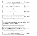
図4は、本発明の実施形態2に係るSOI基板製造方法のフローチャートである。図5Aから図5Gは、図4に示される実施形態に係るSOI基板製造方法における基板構造の概略図である。本実施形態で提供されるSOI基板製造方法は以下のステップを含む。
[Embodiment 2]
FIG. 4 is a flowchart of the SOI substrate manufacturing method according to the second embodiment of the present invention. 5A to 5G are schematic views of the substrate structure in the SOI substrate manufacturing method according to the embodiment shown in FIG. The SOI substrate manufacturing method provided in the present embodiment includes the following steps.
S200:第一のシリコン基板上に第一の酸化層を形成するステップ S200: forming a first oxide layer on the first silicon substrate.
図5Aを参照すると、本実施形態では、まず、二つのシリコン基板、具体的には第一のシリコン基板110及び第二のシリコン基板210(図5Aに示さず)を提供し得る。SOI基板の基本構造において、酸化層は二つのシリコン基板の間に加えられるものであるので、本実施形態の特定の実施では、第一の酸化層121を第一のシリコン基板110上に形成し得て、一般的には、第一のシリコン基板110に対して熱酸化処理を行って、シリコン表面上に第一の酸化層121を形成し得る。
Referring to FIG. 5A, in the present embodiment, first, two silicon substrates, specifically, a
S210:第一のシリコン基板に対してイオン注入を行い、第一のシリコン基板のシリコン層内に欠陥層を形成するステップ S210: performing ion implantation on the first silicon substrate to form a defect layer in the silicon layer of the first silicon substrate.
図5Bを参照すると、本実施形態では、第一の酸化層121が既に成長している第一のシリコン基板110に対してイオン注入を行い、一般的には、高エネルギーイオン注入を行い得て、イオンビーム140aを或る量のエネルギーを用いて第一のシリコン基板110内に誘導して、イオンビームが、第一の酸化層121と、第一のシリコン基板110の一部とを貫通することができ、そして、更に第一のシリコン基板110内の或る深さにおいてシリコンと反応して、その深さに欠陥層140を形成する。欠陥層140の深さは、イオンビーム140aの入射エネルギーに依存する。
Referring to FIG. 5B, in this embodiment, ion implantation may be performed on the
S220:第一のシリコン基板の第一の酸化層上にパターン化エッチストップ層を形成するステップ S220: forming a patterned etch stop layer on the first oxide layer of the first silicon substrate.
特に、S220の具体的な実施については、実施形態1のS110を参照されたい。 In particular, for the specific implementation of S220, refer to S110 of the first embodiment.
任意で、本実施形態のS220は、第一のシリコン基板110の第一の酸化層121上にエッチストップ層130を形成するステップと、エッチストップ層130上にパターン化マスクを形成するステップと、エッチング法を用いてパターン化エッチストップ層130を得るステップと、を含み得る。パターン化マスクは、極紫外線リソグラフィ(Extreme Ultraviolet,略してEUV)法を用いて得られるパターン化フォトレジストを含み、フィーチャサイズが20nm未満であるパターンをEUVフォトリソグラフィ法を用いて生成され得る。
Optionally, S220 of this embodiment includes forming an
図5Cを参照すると、本実施形態では、フォトリソグラフィ技術を用いてパターン化エッチストップ層130を形成し、成長させたエッチストップ層130上にパターン化マスクを形成する。具体的には、パターンサイズが極めて小さいフォトレジストパターン150が、EUVへの露光及び現像の後で、エッチストップ層130上に形成され得る。図5Dを参照すると、フォトレジストパターン150をマスクとして用いて第一のシリコン基板110をエッチングし、フォトレジストパターン150によって覆われていないエッチストップ層130の一部をエッチングして、パターン化エッチストップ層130を形成する。
Referring to FIG. 5C, in the present embodiment, a patterned
パターン化エッチストップ層130の物質は、第一の酸化層121に対してエッチング選択性を有する物質であり、一般的には、窒化シリコン、酸化アルミニウム、酸化チタン、シリコンの豊富な酸化シリコン、水素の豊富な窒化シリコン等の物質が挙げられ、これらの物質は第一の酸化層121に対して高いエッチング選択比を有し得る点に留意されたい。
The material of the patterned
本実施形態の他の可能な実施方式では、パターン化マスクは多孔質アルミナフィルムでもあり得る。この実施方式では、フォトリソグラフィ技術は必要とされず、パターン化処理のために、多孔質アルミナフィルムをエッチストップ層130上に直接積層させる。これまでの実施形態と同様に、本実施形態においても、パターン化マスクのパターンサイズは20nm未満であり得て、パターン化エッチストップ層130のパターンサイズも20nm未満であり得る。
In another possible implementation of this embodiment, the patterned mask can also be a porous alumina film. In this implementation, no photolithographic technique is required, and a porous alumina film is deposited directly on the
S230:パターン化エッチストップ層上に第二の酸化層を成長させて、第二の酸化層に対して平坦化処理及び化学的表面処理を行うステップ S230: Growing a second oxide layer on the patterned etch stop layer and performing planarization treatment and chemical surface treatment on the second oxide layer
図5Eを参照すると、本実施形態では、第一のシリコン基板110の第一の酸化層121上に形成されたパターン化エッチストップ層130は、表面が突出している小型パターンであり、パターン化エッチストップ層130の表面と第二のシリコン基板210との間の結合プロセスを直接行うことができない。従って、第二の酸化層122をパターン化エッチストップ層130上に更に成長させ得て、更に成長させた第二の酸化層122に対して平坦化処理及び化学的表面処理を行って、第一のシリコン基板110が平滑な表面を有するようにし得る。
Referring to FIG. 5E, in the present embodiment, the patterned
第一の酸化層121及び第二の酸化層122は酸化シリコン物質製であり得て、第二の酸化層122の厚さは50nm未満であり得て、第二の酸化層122及び第一の酸化層121のフィルム物質は一般的に同じであり、第二の酸化層122は、パターン化エッチストップ層130の窓領域130a内において第一の酸化層121に接続されて、一体構造を有する酸化層を形成する。
The
S240:パターン化エッチストップ層を有する第一のシリコン基板の表面を第二のシリコン基板の表面に結合させて、第一のシリコン基板の一部を剥離させて、パターン化SOI基板を形成するステップ S240: bonding the surface of the first silicon substrate having the patterned etch stop layer to the surface of the second silicon substrate and peeling off a part of the first silicon substrate to form a patterned SOI substrate.
特に、S240の結合処理の具体的な実施については、実施形態1のS120を参照されたい。 In particular, for the specific implementation of the combining process in S240, refer to S120 in the first embodiment.
図5Fを参照すると、本実施形態では、第一のシリコン基板110のシリコン層の或る深さに欠陥層140が存在していて、本実施形態で形成される半導体構造は、第一のシリコン層110と第二のシリコン層210との間に酸化層が存在している基板構造である。具体的には、第一の酸化層121と第二の酸化層122との間にパターン化エッチストップ層130が存在している。
Referring to FIG. 5F, in this embodiment, the
図5Gを参照すると、本実施形態では、第一の酸化層121が既に成長している第一のシリコン基板110に対してイオン注入を行って、第一のシリコン層110のシリコン層内に欠陥層140を形成する。欠陥層140が既に形成されている第一のシリコン基板110内においては、欠陥層140とシリコン層110aとの間の分子結合が弱まっていて、シリコン層110aを欠陥層140から剥離させることができ、つまり、上部シリコン層110aを剥離させることができ、欠陥層140も剥離させて、欠陥層140の下の第一のシリコン基板110の一部のみを残す。図5F及び図5Gに示されるように、剥離後には、第一のシリコン基板110のシリコン層110bが残されて、パターン化SOI基板300が得られる。更に、第一のシリコン基板110から剥離されたシリコン層110aを用いて、シリコン基板を研磨法で再び製造し得て、シリコン基板を再利用して、生産コストを削減して、生産利益を改善する。
Referring to FIG. 5G, in the present embodiment, ion implantation is performed on the
S250:低温アニーリング処理を行い、第一のシリコン基板及び第二のシリコン基板の隣接する表面を強固に結合させるステップ S250: performing a low temperature annealing process to firmly bond the adjacent surfaces of the first silicon substrate and the second silicon substrate.
S260:パターン化SOI基板に対して表面研磨処理を行うステップ S260: performing a surface polishing process on the patterned SOI substrate
本実施形態では、既に形成されたパターン化SOI基板300に対してアニーリング処理を更に行って、二つのシリコン基板の隣接する表面、つまり、第一のシリコン基板110の第二の酸化層122の表面及び第二のシリコン基板210の表面を強固に結合させる。更に、パターン化SOI基板300の第一のシリコン基板110のシリコン層110aを剥離させるので、シリコン層110aを剥離させた後に、パターン化SOI基板300に対して多様な表面研磨処理を行い得て、平滑な表面構造が、デバイスを形成する際に多様な処理を行うことを容易にする。
In the present embodiment, the
本実施形態で提供されるSOI基板製造方法によると、パターン化エッチストップ層を第一のシリコン基板の酸化層内に形成して、パターン化エッチストップ層を有する第一のシリコン基板の表面を第二のシリコン基板のシリコン表面と結合させて、第一のシリコン基板の一部を剥離させて、パターン化SOI基板を形成するが、これは、ヘテロエピタキシャル層をSOI基板のシリコン層上に成長させる際に、シリコン層とヘテロエピタキシャル層との間に生じる格子不整合及び熱的不整合によって多量の貫通転位が生じるという従来技術の問題を解決する。本実施形態で提供されるパターン化SOI基板によると、貫通転位を有さないヘテロエピタキシャル層をシリコン基板上に形成することができ、光電デバイスの使用性能及び信頼性を改善する。 According to the SOI substrate manufacturing method provided in the present embodiment, the patterned etch stop layer is formed in the oxide layer of the first silicon substrate, and the surface of the first silicon substrate having the patterned etch stop layer is formed on the first silicon substrate. Combined with the silicon surface of the second silicon substrate, a portion of the first silicon substrate is stripped to form a patterned SOI substrate, which grows a heteroepitaxial layer on the silicon layer of the SOI substrate. In this case, the problem of the prior art that a large amount of threading dislocations are generated due to lattice mismatch and thermal mismatch between the silicon layer and the heteroepitaxial layer is solved. According to the patterned SOI substrate provided in the present embodiment, a heteroepitaxial layer having no threading dislocation can be formed on a silicon substrate, which improves the usage performance and reliability of the photoelectric device.
[実施形態3]
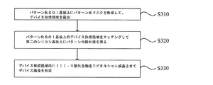
図6は、本発明の実施形態3に係るパターン化SOI基板を用いてヘテロエピタキシャルIII‐V族構造を成長させる方法のフローチャートである。図7Aから図7Eは、図6に示される実施形態に係る技術的工程の概略図である。本実施形態で提供される方法は、これまでの実施形態で提供されたパターン化SOI基板上にヘテロエピタキシャル層を形成する場合に適用可能である。図6に示されるように、本実施形態で提供される方法は以下のステップを含み得る。
[Embodiment 3]
FIG. 6 is a flowchart of a method for growing a heteroepitaxial III-V structure using a patterned SOI substrate according to Embodiment 3 of the present invention. 7A to 7E are schematic diagrams of technical steps according to the embodiment shown in FIG. The method provided in the present embodiment is applicable when forming a heteroepitaxial layer on the patterned SOI substrate provided in the previous embodiments. As shown in FIG. 6, the method provided in the present embodiment may include the following steps.
S310:パターン化SOI基板上にパターン化マスクを形成して、デバイス形成領域を露出させるステップ S310: forming a patterned mask on the patterned SOI substrate to expose a device formation region
図7Aを参照すると、これまでの実施形態に基づき本実施形態で提供されるSOI基板製造方法に従って、パターン化SOI基板300をヘテロエピタキシャル成長させて、光電デバイスを製造するのに適用可能な構造を得る。通常は、多数の独立したデバイスが互いに分離されてこのウェーハ上に製造される。従って、まずは、製造されるデバイスのパターンに従ったデバイス形成領域400をパターン化SOI基板300に設け、製造される光電デバイスをデバイス形成領域400を基板として用いて製造し、パターン化SOI基板300のデバイス形成領域400外の部分は、デバイスを分離するのに用いられ、つまり、デバイス分離領域410である。パターン化SOI基板300をフォトリソグラフィ法を用いてパターン化マスクで処理して、デバイス形成領域400をパターン化マスクの窓部分、つまり、フォトレジスト160によって覆われていない部分内に形成する。
Referring to FIG. 7A, a
S320:パターン化SOI基板上のデバイス形成領域をエッチングして、第二のシリコン基板上にパターン化酸化層を得るステップ S320: etching a device forming region on the patterned SOI substrate to obtain a patterned oxide layer on the second silicon substrate.
図7Bを参照すると、本実施形態では、パターン化SOI基板300のデバイス形成領域400はフォトレジスト160によって覆われておらず、パターン化SOI基板300をエッチングする際に、デバイス形成領域内400の第一のシリコン基板110のシリコン層110bと、第一の酸化層121と、第二の酸化層122の一部とをまずエッチングして、第二のシリコン基板210上のパターン化酸化層123及びパターン化エッチストップ層130を得て、パターン化酸化層123はパターン化エッチストップ層130の下方に存在している。図7Cを参照すると、パターン化SOI基板300のデバイス形成領域400内のパターン化エッチストップ層130を更に除去して、第二のシリコン基板210上にパターン化酸化層123を得る。
Referring to FIG. 7B, in this embodiment, the
デバイス形成領域400内の第一のシリコン基板110のエッチングされたシリコン層110bと、第一の酸化層121と、第二の酸化層122の一部との物質は酸化シリコンであり、パターン化エッチストップ層130の物質はエッチング選択性を有する物質であり得て、一般的に、窒化シリコン、酸化アルミニウム、酸化チタン、シリコンの豊富な酸化シリコン、水素の豊富な窒化シリコン等の物質が挙げられる。特定の実施では、酸化シリコンに対して高い選択比を有するエッチングガスを選択することによって、パターン化エッチストップ層130をほとんどエッチングせずに酸化シリコンをエッチングすることを実現し得る。エッチングガスは、一般的に、高炭素含有量のフッ素系ガス(C2F2やCHF3等)が添加され得て、又は、エッチングガス中の水素含有量を増大させ得る。従って、酸化シリコンをエッチングした後に、第二のシリコン基板210上のパターン化酸化層123及びパターン化エッチストップ層130を形成することができ、パターン化酸化層123は、第二の酸化層122の一部であり、具体的には、パターン化エッチストップ層130によって覆われている第二の酸化層122の一部である。パターン化エッチストップ層130の物質が窒化シリコンである例について説明すると、同様に、窒化シリコンに対して高い選択比を有するエッチングガスを選択して、パターン化酸化層123をほとんどエッチングせずにパターン化エッチストップ層130をエッチングすることを実現する。従って、最終的には、小型パターンを有するパターン化酸化層123が、パターン化SOI基板300のデバイス形成領域400内に得られ、そのパターンは、これまでの実施形態のパターン化エッチストップ層130のパターンサイズと同じサイズを有し、一般的には20nm未満である。エッチングによって形成されるパターン化酸化層123の窓の下部開口は、窓の上部開口よりも一般的に小さいか又は等しく、つまり、窓は垂直な又は傾斜した側壁を有する点に更に留意されたい。
The material of the etched
S330:デバイス形成領域内にIII‐V族化合物をエピタキシャル成長させて、デバイス構造を形成するステップ S330: Step of forming a device structure by epitaxially growing a III-V compound in the device formation region
図7Dを参照すると、本実施形態では、パターン化SOI基板300のデバイス形成領域400内において第二のシリコン基板210上に極めて小さなパターンを有するパターン化酸化層123が存在しているので、ヘテロエピタキシャル層をデバイス形成領域400内に成長し得る。本実施形態では、III‐V族化合物をエピタキシャル成長させる例を用いて説明する。特定の実施では、パターン化酸化層123が既に得られている第二のシリコン基板210上に、第三の酸化層124を成長させ得る。第三の酸化層124をデバイス形成領域400外に成長させて、第三の酸化層124は、III‐V族化合物をエピタキシャル成長させる際にデバイス分離領域410用のマスク機能を提供するのに用いられ、つまり、III‐V族化合物をデバイス形成領域400外の領域に成長させない。図7Eを参照すると、第三の酸化層124が既に成長している第二のシリコン基板210上のパターン化酸化層123上に、III‐V族化合物をエピタキシャル成長させて、デバイス構造170を形成し、第二のシリコン基板210上のパターン化酸化層123のパターン内において、エピタキシャル成長させたIII‐V化合物が第二のシリコン基板210に接続される。具体的には、パターン化酸化層123が第二のシリコン基板210上に存在しているので、貫通転位を有さないIII‐V族化合物エピタキシャル層をデバイス形成領域400内に形成することができる。
Referring to FIG. 7D, in the present embodiment, the patterned
本実施形態のIII‐V族化合物として、例えば、リン化アルミニウムAlP、リン化ガリウムGaP、リン化インジウムInP、ヒ化アルミニウムAlAs、ヒ化ガリウムGaAs、ヒ化インジウムInAs、アンチモン化アルミニウムAlSb、アンチモン化ガリウムGaSb、アンチモン化インジウムInSb、窒化アルミニウムAlN、窒化ガリウムGaN、窒化インジウムInN、これらの三元化合物及び四元化合物が挙げられる点に留意されたい。デバイス形成領域400内にIII‐V族化合物をエピタキシャル成長させる方法として、例えば、分子線エピタキシ(Molecular Beam Epitaxy,略してMBE)法、化学気相堆積(Chemical Vapor Deposition,略してCVD)法、原子層堆積(Atomic Layer Deposition,略してALD)法、又はこれらの変形法が挙げられる。例えば、CVDの変形法として、有機金属化学気相堆積(Metal Organic Chemical Vapor Deposition,略してMOCVD)、プラズマ増強化学気相堆積(Plasma Enhanced Chemical Vapor Deposition,略してPECVD)、低圧化学気相堆積(Low Pressure Chemical Vapor Deposition,略してLPCVD)、超高真空化学気相堆積(Ultra High Vacuum Chemical Vapor Deposition,略してUHVCVD)、減圧化学気相堆積(Reduced Pressure Chemical Vapor Deposition,略してRPCVD)が挙げられる。
Examples of the III-V group compound of this embodiment include aluminum phosphide AlP, gallium phosphide GaP, indium phosphide InP, aluminum arsenide AlAs, gallium arsenide GaAs, indium arsenide InAs, aluminum antimonide AlSb, antimonide Note that gallium GaSb, indium antimonide InSb, aluminum nitride AlN, gallium nitride GaN, indium nitride InN, and their ternary and quaternary compounds. As a method of epitaxially growing a group III-V compound in the
本実施形態で提供されるSOI基板製造方法によると、パターン化エッチストップ層を第一のシリコン基板の酸化層内に形成して、パターン化エッチストップ層を有する第一のシリコン基板の表面を第二のシリコン基板の表面と結合させて、第一のシリコン基板の一部を剥離させて、パターン化SOI基板を形成し、更に、第二のシリコン基板上に小型パターンを有する酸化層を、パターン化エッチストップ層のエッチストップ機能によってパターン化SOI基板上のデバイス形成領域内に形成し、貫通転位を有さないヘテロエピタキシャル層を、第二のシリコン基板上のパターン化酸化層を用いてデバイス形成領域内に成長させることができるが、これは、ヘテロエピタキシャル層をSOI基板のシリコン層上に成長させる際に、シリコン層とヘテロエピタキシャル層との間に生じる格子不整合及び熱的不整合によって多量の貫通転位が生じるという従来技術の問題を解決し、光電デバイスの使用性能及び信頼性を改善する。更に、本実施形態で提供される方法によると、貫通転位を有さないヘテロエピタキシャル層を、デバイス形成領域内でフォトリソグラフィを一回行うだけで成長させることができ、CMOS技術との相性を改善する。 According to the SOI substrate manufacturing method provided in the present embodiment, the patterned etch stop layer is formed in the oxide layer of the first silicon substrate, and the surface of the first silicon substrate having the patterned etch stop layer is formed on the first silicon substrate. Bonding with the surface of the second silicon substrate, a part of the first silicon substrate is peeled off to form a patterned SOI substrate, and an oxide layer having a small pattern is further patterned on the second silicon substrate. A heteroepitaxial layer having no threading dislocation is formed in the device formation region on the patterned SOI substrate by the etch stop function of the patterned etch stop layer, and a device is formed by using the patterned oxide layer on the second silicon substrate. Can be grown in the region, but this is not the case when the heteroepitaxial layer is grown on the silicon layer of the SOI substrate. And solve the problems of the prior art that a large amount of threading dislocations caused by lattice mismatch and thermal mismatch which occurs between the heteroepitaxial layer, to improve the usability and reliability of the photovoltaic device. Furthermore, according to the method provided in the present embodiment, a heteroepitaxial layer having no threading dislocation can be grown by performing photolithography once in the device formation region, thereby improving compatibility with CMOS technology. To do.
更に、本実施形態では、デバイス基板170が既に形成されているパターン化SOI基板300に対してアニーリングプロセスを更に行い得て、デバイス形成領域400内のIII‐V族化合物のエピタキシャル・ラテラル・オーバーグロース(Epitaxial Lateral Overgrowth,略してELO)プロセスにおいて生じる欠陥を減らす。
Furthermore, in the present embodiment, an annealing process can be further performed on the
本実施形態では、貫通転位を有さないヘテロエピタキシャル層をパターン化SOI基板300のデバイス形成領域400内に形成するので、光電デバイス構造をデバイス形成領域400内、つまりはデバイス基板170上に形成することができ、光電デバイス構造は一般的に多層構造を有する。
In the present embodiment, since the heteroepitaxial layer having no threading dislocation is formed in the
図3Bを参照すると、図3Bは本発明の一実施形態に係るSOI基板の概略構造図でもある。そのSOI基板は、図1に示される実施形態で提供されるSOI基板製造方法を用いて製造され得るものであり、実施プロセス及び利点は同じであるので、ここでは再び説明しない。 Referring to FIG. 3B, FIG. 3B is a schematic structural diagram of an SOI substrate according to an embodiment of the present invention. The SOI substrate can be manufactured using the SOI substrate manufacturing method provided in the embodiment shown in FIG. 1, and since the implementation process and advantages are the same, they will not be described again here.
図5Gを参照すると、図5Gは本発明の一実施形態に係る他のSOI基板の概略構造図である。そのSOI基板は、図4に示される実施形態で提供されるSOI基板製造方法を用いて製造され得るものであり、実施プロセス及び利点は同じであるので、ここでは再び説明しない。 Referring to FIG. 5G, FIG. 5G is a schematic structural diagram of another SOI substrate according to an embodiment of the present invention. The SOI substrate can be manufactured using the SOI substrate manufacturing method provided in the embodiment shown in FIG. 4 and the implementation process and advantages are the same and will not be described again here.
図7Eを参照すると、図7Eは本発明の一実施形態に係る更に他のSOI基板の概略構造図である。そのSOI基板は、図6に示される実施形態で提供されるSOI基板製造方法を用いて製造され得るものであり、実施プロセス及び利点は同じであるので、ここでは再び説明しない。 Referring to FIG. 7E, FIG. 7E is a schematic structural diagram of still another SOI substrate according to an embodiment of the present invention. The SOI substrate can be manufactured using the SOI substrate manufacturing method provided in the embodiment shown in FIG. 6 and the implementation process and advantages are the same and will not be described again here.
最後に、以上の実施形態は単に本発明の技術的解決策を説明するためだけのものであり、本発明を限定するものではない点に留意されたい。以上の実施形態を参照して本発明を詳細に説明してきたが、当業者は、本発明の実施形態の技術的解決策の範囲から逸脱せずに、以上の実施形態で説明された技術的解決策を更に修正し得て、また、その技術的特徴の一部又は全部を均等物に置換し得るものである。 Finally, it should be noted that the above embodiments are merely illustrative of the technical solutions of the present invention and do not limit the present invention. Although the present invention has been described in detail with reference to the above embodiments, those skilled in the art will be able to understand the technical aspects described in the above embodiments without departing from the scope of the technical solutions of the embodiments of the present invention. The solution can be further modified and some or all of its technical features can be replaced by equivalents.
第一の態様の第一の可能な実施方式に従う第二の可能な実施方式では、第一のシリコン基板の第一の酸化層上にパターン化エッチストップ層を形成するステップは、
第一のシリコン基板の第一の酸化層上にエッチストップ層を形成するステップと、
エッチストップ層上にパターン化マスクを形成して、エッチングによってパターン化エッチストップ層を得るステップと、を含み、パターン化マスクは、極紫外線(Extreme UltraViolet,EUV)リソグラフィ法を用いて得られるパターン化フォトレジストを含む。
In a second possible implementation according to the first possible implementation of the first aspect, the step of forming a patterned etch stop layer on the first oxide layer of the first silicon substrate comprises:
Forming an etch stop layer on the first oxide layer of the first silicon substrate;
Forming a patterned mask on the etch stop layer to obtain a patterned etch stop layer by etching, wherein the patterned mask is obtained using an extreme ultraviolet (EUV) lithography method Includes photoresist.
第一の態様の第八又は第九の可能な実施方式に従う第十の可能な実施方式では、デバイス形成領域内にIII‐V族化合物をエピタキシャル成長させて、デバイス構造を形成するステップは、
パターン化酸化層が既に得られている第二のシリコン基板上に第三の酸化層を成長させるステップであって、第三の酸化層が前記デバイス形成領域外に成長する、ステップと、
第三の酸化層が既に成長している第二のシリコン基板のパターン化酸化層上にIII‐V族化合物をエピタキシャル成長させて、デバイス構造を形成するステップと、を含み、エピタキシャル成長させたIII‐V族化合物は、第二のシリコン基板のパターン化酸化層のパターン内において第二のシリコン基板に接続される。
In a tenth possible implementation manner according to the eighth or ninth possible implementation manner of the first aspect, the step of epitaxially growing a group III-V compound in the device formation region to form the device structure comprises:
Growing a third oxide layer on a second silicon substrate from which a patterned oxide layer has already been obtained, wherein the third oxide layer is grown outside the device formation region;
Epitaxially growing a III-V compound on a patterned oxide layer of a second silicon substrate on which a third oxide layer has already been grown to form a device structure, and epitaxially growing the III-V The group compound is connected to the second silicon substrate in the pattern of the patterned oxide layer of the second silicon substrate.
第一の態様の第八から第十の可能な実施方式のうちいずれか一つに従う第十一の可能な実施方式では、III‐V族化合物は、リン化アルミニウム(aluminium phosphide,AlP)、リン化ガリウム(gallium phosphide,GaP)、リン化インジウム(indium phosphide,InP)、ヒ化アルミニウム(aluminium arsenide,AlAs)、ヒ化ガリウム(gallium arsenide,GaAs)、ヒ化インジウム(indium arsenide,InAs)、アンチモン化アルミニウム(aluminium antimonide,AlSb)、アンチモン化ガリウム(gallium antimonide,GaSb)、アンチモン化インジウム(indium antimonide,InSb)、窒化アルミニウム(aluminium nitride,AlN)、窒化ガリウム(gallium nitride,GaN)、窒化インジウム(indium nitride,InN)、又は、これらの三元化合物及び四元化合物を含む。 In an eleventh possible implementation according to any one of the eighth to tenth possible implementations of the first aspect, the group III-V compound is aluminum phosphide (AlP) , phosphorous Gallium phosphide (GaP) , Indium phosphide (InP) , Aluminum arsenide (AlAs) , Gallium arsenide (GaAs) , Indium arsenide, InAs Aluminum antimonide (AlSb) , gallium antimonide (GaSb) , indium antimonide ( Indium antimonide ( InSb) , aluminum nitride (AlN) , gallium nitride (gallium nitride, GaN) , indium nitride (indium nitride, InN) , or a ternary compound and a quaternary compound thereof.
第一の態様の第八から第十一の可能な実施方式のうちいずれか一つに従う第十二の可能な実施方式では、デバイス形成領域内にIII‐V族化合物をエピタキシャル成長させて、デバイス構造を形成するステップは、
分子線エピタキシ(molecular beam epitaxy,MBE)法、化学気相堆積(chemical vapor deposition,CVD)法、原子層堆積ALD法、又はこれらの変形法を用いて、デバイス形成領域内にIII‐V族化合物を成長させて、デバイス構造を形成するステップを含む。
In a twelfth possible implementation manner according to any one of the eighth to eleventh possible implementation manners of the first aspect, a III-V compound is epitaxially grown in the device formation region to produce a device structure. The step of forming
Using a molecular beam epitaxy (MBE) method, a chemical vapor deposition (CVD) method, an atomic layer deposition ALD method, or a modified method thereof, a group III-V compound is formed in the device formation region. Growing a device structure to form a device structure .
第一の態様の第八から第十二の可能な実施方式のうちいずれか一つに従う第十三の可能な実施方式では、本方法は、
デバイス構造が既に形成されているパターン化SOI基板に対してアニーリング処理を行い、デバイス形成領域内におけるIII‐V族化合物のエピタキシャル・ラテラル・オーバーグロースELOによって生じる欠陥を減らすステップを更に含む。
In a thirteenth possible implementation manner according to any one of the eighth to twelfth possible implementation manners of the first aspect, the method comprises:
The method further includes performing an annealing process on the patterned SOI substrate on which the device structure has already been formed to reduce defects caused by the epitaxial lateral overgrowth ELO of the III-V compound in the device formation region.
以下、本実施形態又は従来技術を説明するのに必要な添付図面について簡単に説明する。 The following briefly describes the accompanying drawings required for describing the present embodiment or the related art .
以下、本発明の実施形態の添付図面を参照して、本発明の実施形態の技術的解決策を説明する。 Hereinafter, with reference to the accompanying drawings embodiments of the present invention, to explain the technical solutions of the embodiments of the present invention.
[実施形態1]
図1は、本発明の実施形態1に係るSOI基板製造方法のフローチャートである。本実施形態の方法は、半導体デバイス構造の製造の場合に適用可能である。本実施形態の方法は以下のステップを含む。
[Embodiment 1]
FIG. 1 is a flowchart of an SOI substrate manufacturing method according to
S120:パターン化エッチストップ層を有する第一のシリコン基板の表面を第二のシリコン基板のシリコン表面と結合させて、第一のシリコン基板の一部を剥離させて、パターン化SOI基板を形成するステップ S120: the first surface of the silicon substrate having the patterned etch stop layer is coupled with the second silicon substrate silicon surface, by stripping a part of the first silicon substrate, forming a patterned S OI substrate Step to do
任意で、本実施形態のS220は、第一のシリコン基板110の第一の酸化層121上にエッチストップ層130を形成するステップと、エッチストップ層130上にパターン化マスクを形成するステップと、エッチング法を用いてパターン化エッチストップ層130を得るステップと、を含み得る。パターン化マスクは、極紫外線(EUV)リソグラフィ(Extreme Ultraviolet,略してEUV)法を用いて得られるパターン化フォトレジストを含み、フィーチャサイズが20nm未満であるパターンをEUVフォトリソグラフィ法を用いて生成され得る。
Optionally, S220 of this embodiment includes forming an
図7Aを参照すると、これまでの実施形態に基づき本実施形態で提供される方法に従って、パターン化SOI基板300をヘテロエピタキシャル成長させて、光電デバイスを製造するのに適用可能な構造を得る。通常は、多数の独立したデバイスが互いに分離されてこのウェーハ上に製造される。従って、まずは、製造されるデバイスのパターンに従ったデバイス形成領域400をパターン化SOI基板300に設け、製造される光電デバイスをデバイス形成領域400を基板として用いて製造し、パターン化SOI基板300のデバイス形成領域400外の部分は、デバイスを分離するのに用いられ、つまり、デバイス分離領域410である。パターン化SOI基板300をフォトリソグラフィ法を用いてパターン化マスクで処理して、デバイス形成領域400をパターン化マスクの窓部分、つまり、フォトレジスト160によって覆われていない部分内に形成する。
Referring to FIG. 7A, obtained according to how Ru are provided in this embodiment on the basis of the previous embodiments, the
本実施形態のIII‐V族化合物として、例えば、AlP、GaP、InP、AlAs、GaAs、InAs、AlSb、GaSb、InSb、AlN、GaN、InN、これらの三元化合物及び四元化合物が挙げられる点に留意されたい。デバイス形成領域400内にIII‐V族化合物をエピタキシャル成長させる方法として、例えば、分子線エピタキシ(Molecular Beam Epitaxy,MBE)法、化学気相堆積(Chemical Vapor Deposition,CVD)法、原子層堆積(Atomic Layer Deposition,ALD)法、又はこれらの変形法が挙げられる。例えば、CVDの変形法として、有機金属化学気相堆積(Metal Organic Chemical Vapor Deposition,MOCVD)、プラズマ増強化学気相堆積(Plasma Enhanced Chemical Vapor Deposition,PECVD)、低圧化学気相堆積(Low Pressure Chemical Vapor Deposition,LPCVD)、超高真空化学気相堆積(Ultra High Vacuum Chemical Vapor Deposition,UHVCVD)、減圧化学気相堆積(Reduced Pressure Chemical Vapor Deposition,RPCVD)が挙げられる。
Examples of the III-V group compound of this embodiment include AlP, GaP, InP, AlAs, GaAs, InAs, AlSb, GaSb, InSb, AlN, GaN, InN , and their ternary and quaternary compounds. Please note that. As a method of epitaxially growing a group III-V compound to the
本実施形態で提供される方法によると、パターン化エッチストップ層を第一のシリコン基板の酸化層内に形成して、パターン化エッチストップ層を有する第一のシリコン基板の表面を第二のシリコン基板の表面と結合させて、第一のシリコン基板の一部を剥離させて、パターン化SOI基板を形成し、更に、第二のシリコン基板上に小型パターンを有する酸化層を、パターン化エッチストップ層のエッチストップ機能によってパターン化SOI基板上のデバイス形成領域内に形成し、貫通転位を有さないヘテロエピタキシャル層を、第二のシリコン基板上のパターン化酸化層を用いてデバイス形成領域内に成長させることができるが、これは、ヘテロエピタキシャル層をSOI基板のシリコン層上に成長させる際に、シリコン層とヘテロエピタキシャル層との間に生じる格子不整合及び熱的不整合によって多量の貫通転位が生じるという従来技術の問題を解決し、光電デバイスの使用性能及び信頼性を改善する。更に、本実施形態で提供される方法によると、貫通転位を有さないヘテロエピタキシャル層を、デバイス形成領域内でフォトリソグラフィを一回行うだけで成長させることができ、CMOS技術との相性を改善する。 According to how Ru are provided in this embodiment, the patterned etch stop layer first formed in the oxide layer in the silicon substrate, the first silicon substrate having a patterned etch stop layer surface a second Bonded with the surface of the silicon substrate, a part of the first silicon substrate is peeled off to form a patterned SOI substrate, and an oxide layer having a small pattern is formed on the second silicon substrate by pattern etching. A heteroepitaxial layer having no threading dislocation is formed in the device formation region on the patterned SOI substrate by the etch stop function of the stop layer, and the heteroepitaxial layer having no threading dislocation is formed in the device formation region by using the patterned oxide layer on the second silicon substrate. This is because when the heteroepitaxial layer is grown on the silicon layer of the SOI substrate, Solves the problems of the prior art that a large amount of threading dislocations caused by lattice mismatch and thermal mismatch which occurs between the Kisharu layer, to improve the usability and reliability of the photovoltaic device. Furthermore, according to the method provided in the present embodiment, a heteroepitaxial layer having no threading dislocation can be grown by performing photolithography once in the device formation region, thereby improving compatibility with CMOS technology. To do.
更に、本実施形態では、デバイス構造170が既に形成されているパターン化SOI基板300に対してアニーリングプロセスを更に行い得て、デバイス形成領域400内のIII‐V族化合物のエピタキシャル・ラテラル・オーバーグロース(Epitaxial Lateral Overgrowth,略してELO)プロセスにおいて生じる欠陥を減らす。
Furthermore, in the present embodiment, an annealing process can be further performed on the
本実施形態では、貫通転位を有さないヘテロエピタキシャル層をパターン化SOI基板300のデバイス形成領域400内に形成するので、光電デバイス構造をデバイス形成領域400内、つまりはデバイス構造170上に形成することができ、光電デバイス構造は一般的に多層構造を有する。
In the present embodiment, since the heteroepitaxial layer having no threading dislocation is formed in the
Claims (16)
第一のシリコン基板の酸化層内にパターン化エッチストップ層を形成するステップと、
前記パターン化エッチストップ層を有する前記第一のシリコン基板の表面を第二のシリコン基板の表面と結合させて、前記第一のシリコン基板の一部を剥離させて、パターン化シリコン・オン・インシュレータSOI基板を形成するステップと、を備える方法。 An SOI substrate manufacturing method comprising:
Forming a patterned etch stop layer in the oxide layer of the first silicon substrate;
A surface of the first silicon substrate having the patterned etch stop layer is bonded to a surface of a second silicon substrate, and a part of the first silicon substrate is peeled off to form a patterned silicon-on-insulator. Forming an SOI substrate.
前記第一のシリコン基板上に第一の酸化層を形成するステップと、
前記第一のシリコン基板の前記第一の酸化層上に前記パターン化エッチストップ層を形成するステップと、を備える、請求項1に記載の方法。 Forming a patterned etch stop layer in the oxide layer of the first silicon substrate;
Forming a first oxide layer on the first silicon substrate;
Forming the patterned etch stop layer on the first oxide layer of the first silicon substrate.
前記第一のシリコン基板の前記第一の酸化層上にエッチストップ層を形成するステップと、
前記エッチストップ層上にパターン化マスクを形成し、エッチングによって前記パターン化エッチストップ層を得るステップと、を備え、前記パターン化マスクが、極紫外線リソグラフィEUV法を用いて得られるパターン化フォトレジストを備える、請求項2に記載の方法。 Forming the patterned etch stop layer on the first oxide layer of the first silicon substrate;
Forming an etch stop layer on the first oxide layer of the first silicon substrate;
Forming a patterned mask on the etch stop layer and obtaining the patterned etch stop layer by etching, wherein the patterned mask comprises a patterned photoresist obtained by using an extreme ultraviolet lithography EUV method. The method of claim 2 comprising.
前記第一のシリコン基板の前記第一の酸化層上にエッチストップ層を形成するステップと、
前記エッチストップ層上にパターン化マスクを形成し、エッチングによって前記パターン化エッチストップ層を得るステップと、を備え、前記パターン化マスクが多孔質アルミナフィルムを備える、請求項2に記載の方法。 Forming the patterned etch stop layer on the first oxide layer of the first silicon substrate;
Forming an etch stop layer on the first oxide layer of the first silicon substrate;
Forming a patterned mask on the etch stop layer and obtaining the patterned etch stop layer by etching, wherein the patterned mask comprises a porous alumina film.
前記パターン化エッチストップ層上に第二の酸化層を成長させ、前記第二の酸化層に対して平坦化処理及び化学的表面処理を行うステップを更に備える請求項2から4のいずれか一項に記載の方法。 After forming the patterned etch stop layer on the first oxide layer of the first silicon substrate,
5. The method according to claim 2, further comprising: growing a second oxide layer on the patterned etch stop layer, and performing a planarization process and a chemical surface treatment on the second oxide layer. The method described in 1.
前記第一のシリコン基板に対してイオン注入を行い、前記第一のシリコン基板のシリコン層内に欠陥層を形成するステップを更に備え、前記第一のシリコン基板の一部を剥離させることが、前記第一のシリコン基板内の前記欠陥層と、前記欠陥層上のシリコン層とを剥離させることを備え、
前記パターン化エッチストップ層を有する前記第一のシリコン基板の表面を第二のシリコン基板のシリコン表面と結合させて、前記第一のシリコン基板の一部を剥離させて、パターン化シリコン・オン・インシュレータSOI基板を形成するステップの後に、
低温アニーリング処理を行い、前記第一のシリコン基板及び前記第二のシリコン基板の隣接した表面を強固に結合させるステップと、
前記パターン化SOI基板に対して表面研磨処理を行うステップと、を更に備える請求項2から5のいずれか一項に記載の方法。 Prior to forming the patterned etch stop layer on the first oxide layer of the first silicon substrate,
Performing ion implantation on the first silicon substrate to further form a defect layer in the silicon layer of the first silicon substrate, and peeling a part of the first silicon substrate; Peeling off the defect layer in the first silicon substrate and the silicon layer on the defect layer;
Bonding the surface of the first silicon substrate having the patterned etch stop layer with the silicon surface of a second silicon substrate and peeling off a portion of the first silicon substrate to form a patterned silicon on After the step of forming the insulator SOI substrate,
Performing a low temperature annealing process to firmly bond adjacent surfaces of the first silicon substrate and the second silicon substrate;
The method according to claim 2, further comprising performing a surface polishing process on the patterned SOI substrate.
前記パターン化SOI基板上の前記デバイス形成領域をエッチングして、前記第二のシリコン基板上にパターン化酸化層を得るステップと、
前記デバイス形成領域内にIII‐V族化合物をエピタキシャル成長させて、デバイス構造を形成するステップと、を更に備える請求項1から8のいずれか一項に記載の方法。 Forming a patterned mask on the patterned SOI substrate to expose a device formation region;
Etching the device formation region on the patterned SOI substrate to obtain a patterned oxide layer on the second silicon substrate;
The method according to claim 1, further comprising epitaxially growing a group III-V compound in the device formation region to form a device structure.
前記パターン化SOI基板上の前記デバイス形成領域内の前記第一のシリコン基板のシリコン層と、前記第一の酸化層と、前記第二の酸化層の一部とをエッチングして、前記第二のシリコン基板上の前記パターン化酸化層及び前記パターン化エッチストップ層を得るステップであって、前記パターン化酸化層が前記パターン化エッチストップ層の下に存在する、ステップと、
前記パターン化SOI基板上の前記デバイス形成領域内の前記パターン化エッチストップ層を除去して、前記第二のシリコン基板上に前記パターン化酸化層を得るステップと、を備える、請求項9に記載の方法。 Etching the device forming region on the patterned SOI substrate to obtain a patterned oxide layer on the second silicon substrate;
Etching the silicon layer of the first silicon substrate, the first oxide layer, and a portion of the second oxide layer in the device formation region on the patterned SOI substrate, Obtaining the patterned oxide layer on the silicon substrate and the patterned etch stop layer, wherein the patterned oxide layer is present under the patterned etch stop layer;
Removing the patterned etch stop layer in the device formation region on the patterned SOI substrate to obtain the patterned oxide layer on the second silicon substrate. the method of.
前記パターン化酸化層が既に得られている前記第二のシリコン基板上に第三の酸化層を成長させるステップであって、前記第三の酸化層が前記デバイス形成領域外に成長する、ステップと、
前記第三の酸化層が既に成長している前記第二のシリコン基板の前記パターン化酸化層上に前記III‐V族化合物をエピタキシャル成長させて、前記デバイス構造を形成するステップと、を備え、エピタキシャル成長させた前記III‐V族化合物が前記第二のシリコン基板の前記パターン化酸化層のパターン内において前記第二のシリコン基板に接続される、請求項9又は10に記載の方法。 Epitaxially growing a group III-V compound in the device formation region to form a device substrate;
Growing a third oxide layer on the second silicon substrate from which the patterned oxide layer has already been obtained, wherein the third oxide layer is grown outside the device formation region; and ,
Epitaxially growing the III-V compound on the patterned oxide layer of the second silicon substrate on which the third oxide layer has already been grown to form the device structure. The method according to claim 9 or 10, wherein the group III-V compound is connected to the second silicon substrate in a pattern of the patterned oxide layer of the second silicon substrate.
分子線エピタキシMBE法、化学気相堆積CVD法、原子層堆積ALD法、又はこれらの変形法を用いて、前記デバイス形成領域内に前記III‐V族化合物を成長させて、前記デバイス基板を形成するステップを備える、請求項9から12のいずれか一項に記載の方法。 Epitaxially growing a group III-V compound in the device formation region to form a device substrate;
Using the molecular beam epitaxy MBE method, the chemical vapor deposition CVD method, the atomic layer deposition ALD method, or a modified method thereof, the III-V group compound is grown in the device formation region to form the device substrate. The method according to any one of claims 9 to 12, comprising the step of:
Applications Claiming Priority (1)
| Application Number | Priority Date | Filing Date | Title |
|---|---|---|---|
| PCT/CN2014/071108 WO2015109456A1 (en) | 2014-01-22 | 2014-01-22 | Soi substrate manufacturing method and soi substrate |
Publications (2)
| Publication Number | Publication Date |
|---|---|
| JP2017510060A true JP2017510060A (en) | 2017-04-06 |
| JP6264675B2 JP6264675B2 (en) | 2018-01-24 |
Family
ID=53680571
Family Applications (1)
| Application Number | Title | Priority Date | Filing Date |
|---|---|---|---|
| JP2016547879A Active JP6264675B2 (en) | 2014-01-22 | 2014-01-22 | Silicon-on-insulator (SOI) substrate manufacturing method and SOI substrate |
Country Status (6)
| Country | Link |
|---|---|
| US (1) | US10804137B2 (en) |
| EP (1) | EP3089205B1 (en) |
| JP (1) | JP6264675B2 (en) |
| CN (1) | CN105340074B (en) |
| RU (1) | RU2639612C1 (en) |
| WO (1) | WO2015109456A1 (en) |
Families Citing this family (8)
| Publication number | Priority date | Publication date | Assignee | Title |
|---|---|---|---|---|
| CN105392089A (en) * | 2015-12-03 | 2016-03-09 | 瑞声声学科技(深圳)有限公司 | Composite layer structure and manufacture method thereof |
| CN105392093B (en) * | 2015-12-03 | 2018-09-11 | 瑞声声学科技(深圳)有限公司 | The manufacturing method of microphone chip |
| US10304749B2 (en) * | 2017-06-20 | 2019-05-28 | Intel Corporation | Method and apparatus for improved etch stop layer or hard mask layer of a memory device |
| KR102374206B1 (en) | 2017-12-05 | 2022-03-14 | 삼성전자주식회사 | Method of fabricating semiconductor device |
| CN113512697A (en) * | 2020-04-10 | 2021-10-19 | 中国科学技术大学 | High-precision silicon-based mask plate and processing method thereof |
| CN111880124B (en) * | 2020-07-10 | 2021-11-19 | 中国科学院上海微系统与信息技术研究所 | Preparation method of high-frequency adjustable magnetic field detector |
| RU2745297C1 (en) * | 2020-08-05 | 2021-03-23 | Обществом с ограниченной ответственностью "Маппер" | Device for manual alignment of silicon wafers prior to temporary splicing |
| US20240194670A1 (en) * | 2022-12-09 | 2024-06-13 | International Business Machines Corporation | Asymmetrically bonded integrated circuit devices |
Citations (6)
| Publication number | Priority date | Publication date | Assignee | Title |
|---|---|---|---|---|
| JPH0484418A (en) * | 1990-07-27 | 1992-03-17 | Nec Corp | Method of heteroepitaxial development of iii-v group compound semiconductor for different types of substrates |
| JPH11111839A (en) * | 1997-10-01 | 1999-04-23 | Denso Corp | Semiconductor substrate and method of manufacturing the same |
| JP2000030996A (en) * | 1998-07-07 | 2000-01-28 | Shin Etsu Handotai Co Ltd | SOI wafer manufacturing method and SOI wafer |
| US6191007B1 (en) * | 1997-04-28 | 2001-02-20 | Denso Corporation | Method for manufacturing a semiconductor substrate |
| US20030048395A1 (en) * | 2001-08-27 | 2003-03-13 | Seiko Epson Corporation | Electric optical apparatus and manufacturing method of the same, projection display, and electronic instrument |
| US20120028444A1 (en) * | 2010-07-29 | 2012-02-02 | Taiwan Semiconductor Manufacturing Company, Ltd. | Defect-free hetero-epitaxy of lattice mismatched semiconductors |
Family Cites Families (23)
| Publication number | Priority date | Publication date | Assignee | Title |
|---|---|---|---|---|
| US5935762A (en) * | 1997-10-14 | 1999-08-10 | Industrial Technology Research Institute | Two-layered TSI process for dual damascene patterning |
| KR100318467B1 (en) * | 1998-06-30 | 2002-02-19 | 박종섭 | A method of fabricating bonding type SOI wafer |
| US6881645B2 (en) * | 2000-08-17 | 2005-04-19 | Samsung Electronics Co., Ltd. | Method of preventing semiconductor layers from bending and semiconductor device formed thereby |
| CN1315155C (en) * | 2004-03-19 | 2007-05-09 | 中国科学院上海微系统与信息技术研究所 | Upper silicon structure of insulation layer and its prepn. method |
| US7138309B2 (en) * | 2005-01-19 | 2006-11-21 | Sharp Laboratories Of America, Inc. | Integration of biaxial tensile strained NMOS and uniaxial compressive strained PMOS on the same wafer |
| US8324660B2 (en) * | 2005-05-17 | 2012-12-04 | Taiwan Semiconductor Manufacturing Company, Ltd. | Lattice-mismatched semiconductor structures with reduced dislocation defect densities and related methods for device fabrication |
| KR100705225B1 (en) | 2005-12-15 | 2007-04-06 | 엘지전자 주식회사 | Manufacturing method of vertical light emitting device |
| TWI334164B (en) * | 2006-06-07 | 2010-12-01 | Ind Tech Res Inst | Method of manufacturing nitride semiconductor substrate and composite material substrate |
| FR2906078B1 (en) * | 2006-09-19 | 2009-02-13 | Commissariat Energie Atomique | METHOD FOR MANUFACTURING A MIXED MICRO-TECHNOLOGICAL STRUCTURE AND A STRUCTURE THUS OBTAINED |
| KR20080093624A (en) * | 2007-04-17 | 2008-10-22 | 삼성전자주식회사 | Multiple dielectric film for semiconductor device and method for fabricating the same |
| US7795132B2 (en) * | 2007-07-31 | 2010-09-14 | Molecular Imprints, Inc. | Self-aligned cross-point memory fabrication |
| CN100592533C (en) * | 2007-10-15 | 2010-02-24 | 天钰科技股份有限公司 | laterally diffused metal oxide transistor |
| US7883956B2 (en) * | 2008-02-15 | 2011-02-08 | International Business Machines Corporation | Method of forming coplanar active and isolation regions and structures thereof |
| RU2368034C1 (en) * | 2008-05-13 | 2009-09-20 | Институт физики полупроводников Сибирского отделения Российской академии наук | Method for manufacturing of silicon-on-insulator structure |
| WO2009152648A1 (en) * | 2008-06-20 | 2009-12-23 | Lee Tienhsi | Method for the production of thin film |
| CN100585805C (en) * | 2008-10-10 | 2010-01-27 | 上海新傲科技有限公司 | Method for preparing silicon-on-insulator substrate |
| US7767546B1 (en) * | 2009-01-12 | 2010-08-03 | International Business Machines Corporation | Low cost fabrication of double box back gate silicon-on-insulator wafers with built-in shallow trench isolation in back gate layer |
| US7994550B2 (en) * | 2009-05-22 | 2011-08-09 | Raytheon Company | Semiconductor structures having both elemental and compound semiconductor devices on a common substrate |
| DE102009051520B4 (en) * | 2009-10-31 | 2016-11-03 | X-Fab Semiconductor Foundries Ag | Process for the production of silicon semiconductor wafers with layer structures for the integration of III-V semiconductor devices |
| US20120168823A1 (en) * | 2010-12-31 | 2012-07-05 | Zhijiong Luo | Semiconductor device and method for manufacturing the same |
| CN102332423B (en) * | 2011-05-25 | 2013-11-06 | 湖南红太阳光电科技有限公司 | Process for reducing chemical-mechanical polishing crack on buried layer cavity silicon-on-insulator (SOI) wafer |
| RU2497231C1 (en) * | 2012-04-19 | 2013-10-27 | Федеральное государственное бюджетное учреждение науки Институт физики полупроводников им. А.В. Ржанова Сибирского отделения Российской академии наук (ИФП СО РАН) | Method for making silicon-on-insulator structure |
| KR102284657B1 (en) * | 2015-01-05 | 2021-08-02 | 삼성전자 주식회사 | Photodiode and optical communication system including the same |
-
2014
- 2014-01-22 RU RU2016134085A patent/RU2639612C1/en active
- 2014-01-22 JP JP2016547879A patent/JP6264675B2/en active Active
- 2014-01-22 EP EP14879857.2A patent/EP3089205B1/en active Active
- 2014-01-22 CN CN201480037255.3A patent/CN105340074B/en active Active
- 2014-01-22 WO PCT/CN2014/071108 patent/WO2015109456A1/en not_active Ceased
-
2016
- 2016-07-19 US US15/214,257 patent/US10804137B2/en active Active
Patent Citations (8)
| Publication number | Priority date | Publication date | Assignee | Title |
|---|---|---|---|---|
| JPH0484418A (en) * | 1990-07-27 | 1992-03-17 | Nec Corp | Method of heteroepitaxial development of iii-v group compound semiconductor for different types of substrates |
| US6191007B1 (en) * | 1997-04-28 | 2001-02-20 | Denso Corporation | Method for manufacturing a semiconductor substrate |
| JPH11111839A (en) * | 1997-10-01 | 1999-04-23 | Denso Corp | Semiconductor substrate and method of manufacturing the same |
| JP2000030996A (en) * | 1998-07-07 | 2000-01-28 | Shin Etsu Handotai Co Ltd | SOI wafer manufacturing method and SOI wafer |
| US6245645B1 (en) * | 1998-07-07 | 2001-06-12 | Shin-Etsu Handotai Co., Ltd. | Method of fabricating an SOI wafer |
| US20030048395A1 (en) * | 2001-08-27 | 2003-03-13 | Seiko Epson Corporation | Electric optical apparatus and manufacturing method of the same, projection display, and electronic instrument |
| JP2003152193A (en) * | 2001-08-27 | 2003-05-23 | Seiko Epson Corp | Electro-optical device, method of manufacturing electro-optical device, projection display device, and electronic apparatus |
| US20120028444A1 (en) * | 2010-07-29 | 2012-02-02 | Taiwan Semiconductor Manufacturing Company, Ltd. | Defect-free hetero-epitaxy of lattice mismatched semiconductors |
Also Published As
| Publication number | Publication date |
|---|---|
| RU2639612C1 (en) | 2017-12-21 |
| CN105340074A (en) | 2016-02-17 |
| US20160329239A1 (en) | 2016-11-10 |
| WO2015109456A1 (en) | 2015-07-30 |
| JP6264675B2 (en) | 2018-01-24 |
| EP3089205A4 (en) | 2017-01-11 |
| EP3089205A1 (en) | 2016-11-02 |
| EP3089205B1 (en) | 2020-03-18 |
| CN105340074B (en) | 2019-07-19 |
| US10804137B2 (en) | 2020-10-13 |
Similar Documents
| Publication | Publication Date | Title |
|---|---|---|
| JP6264675B2 (en) | Silicon-on-insulator (SOI) substrate manufacturing method and SOI substrate | |
| CN101300663B (en) | Lattice-mismatched semiconductor structures with reduced dislocation defect density and related device fabrication methods | |
| KR102110858B1 (en) | Defect transferred and lattice mismatched epitaxial film | |
| EP2423951B1 (en) | Antiphase domain boundary-free III-V compound semiconductor material on semiconductor substrate and method for manufacturing thereof | |
| KR102106348B1 (en) | Non-silicon device heterolayers on patterned silicon substrate for cmos by combination of selective and conformal epitaxy | |
| CN102790084B (en) | Germanium and III-V mix coplanar soi semiconductor structure and preparation method thereof | |
| US9355889B2 (en) | Semiconductor-on-insulator device and method of fabricating the same | |
| KR20160111364A (en) | Iii-n devices in si trenches | |
| CN102790054A (en) | Germanium and III-V mixed coplanar semi-conductor structure and preparation method thereof | |
| US10204781B1 (en) | Methods for bottom up fin structure formation | |
| CN102593037B (en) | Semiconductor structure and fabrication method thereof | |
| US7687378B2 (en) | Fabricating method of nitride semiconductor substrate and composite material substrate | |
| CN101944538B (en) | Semiconductor structures and manufacturing method thereof | |
| US9917153B2 (en) | Method for producing a microelectronic device | |
| CN103280425B (en) | A kind of compound substrate and manufacture method thereof with separator | |
| TW201729355A (en) | Method of making a hybrid substrate | |
| EP2924722A1 (en) | Method for manufacturing a semiconductor-on-insulator device | |
| CN105745737B (en) | Planar Heterogeneous Devices | |
| KR101566224B1 (en) | SEMICONDUCTOR DEVICE USING Ge AND III-V GROUP COMPOUND SEMICONDUCTOR AND METHOD OF MANUFACTURING THE SAME | |
| US11088244B2 (en) | Devices having substrates with selective airgap regions | |
| CN103855005B (en) | Double stress heterogeneous SOI semiconductor structure and its manufacturing method | |
| Huangfu et al. | Monolithic integration of III–V devices with silicon photonics on a modified SOI platform |
Legal Events
| Date | Code | Title | Description |
|---|---|---|---|
| A521 | Request for written amendment filed |
Free format text: JAPANESE INTERMEDIATE CODE: A523 Effective date: 20160901 |
|
| A621 | Written request for application examination |
Free format text: JAPANESE INTERMEDIATE CODE: A621 Effective date: 20160901 |
|
| A977 | Report on retrieval |
Free format text: JAPANESE INTERMEDIATE CODE: A971007 Effective date: 20170731 |
|
| A131 | Notification of reasons for refusal |
Free format text: JAPANESE INTERMEDIATE CODE: A131 Effective date: 20170808 |
|
| A521 | Request for written amendment filed |
Free format text: JAPANESE INTERMEDIATE CODE: A523 Effective date: 20171108 |
|
| TRDD | Decision of grant or rejection written | ||
| A01 | Written decision to grant a patent or to grant a registration (utility model) |
Free format text: JAPANESE INTERMEDIATE CODE: A01 Effective date: 20171121 |
|
| A61 | First payment of annual fees (during grant procedure) |
Free format text: JAPANESE INTERMEDIATE CODE: A61 Effective date: 20171207 |
|
| R150 | Certificate of patent or registration of utility model |
Ref document number: 6264675 Country of ref document: JP Free format text: JAPANESE INTERMEDIATE CODE: R150 |
|
| R250 | Receipt of annual fees |
Free format text: JAPANESE INTERMEDIATE CODE: R250 |
|
| R250 | Receipt of annual fees |
Free format text: JAPANESE INTERMEDIATE CODE: R250 |
|
| R250 | Receipt of annual fees |
Free format text: JAPANESE INTERMEDIATE CODE: R250 |
|
| R250 | Receipt of annual fees |
Free format text: JAPANESE INTERMEDIATE CODE: R250 |
|
| R250 | Receipt of annual fees |
Free format text: JAPANESE INTERMEDIATE CODE: R250 |
|
| R250 | Receipt of annual fees |
Free format text: JAPANESE INTERMEDIATE CODE: R250 |