JP2019096897A - 半導体装置 - Google Patents
半導体装置 Download PDFInfo
- Publication number
- JP2019096897A JP2019096897A JP2019014714A JP2019014714A JP2019096897A JP 2019096897 A JP2019096897 A JP 2019096897A JP 2019014714 A JP2019014714 A JP 2019014714A JP 2019014714 A JP2019014714 A JP 2019014714A JP 2019096897 A JP2019096897 A JP 2019096897A
- Authority
- JP
- Japan
- Prior art keywords
- conductivity type
- impurity concentration
- semiconductor layer
- peak
- layer
- Prior art date
- Legal status (The legal status is an assumption and is not a legal conclusion. Google has not performed a legal analysis and makes no representation as to the accuracy of the status listed.)
- Granted
Links
Images


Classifications
-
- H—ELECTRICITY
- H10—SEMICONDUCTOR DEVICES; ELECTRIC SOLID-STATE DEVICES NOT OTHERWISE PROVIDED FOR
- H10D—INORGANIC ELECTRIC SEMICONDUCTOR DEVICES
- H10D62/00—Semiconductor bodies, or regions thereof, of devices having potential barriers
- H10D62/10—Shapes, relative sizes or dispositions of the regions of the semiconductor bodies; Shapes of the semiconductor bodies
- H10D62/17—Semiconductor regions connected to electrodes not carrying current to be rectified, amplified or switched, e.g. channel regions
- H10D62/393—Body regions of DMOS transistors or IGBTs
-
- H—ELECTRICITY
- H10—SEMICONDUCTOR DEVICES; ELECTRIC SOLID-STATE DEVICES NOT OTHERWISE PROVIDED FOR
- H10D—INORGANIC ELECTRIC SEMICONDUCTOR DEVICES
- H10D12/00—Bipolar devices controlled by the field effect, e.g. insulated-gate bipolar transistors [IGBT]
- H10D12/411—Insulated-gate bipolar transistors [IGBT]
- H10D12/441—Vertical IGBTs
- H10D12/461—Vertical IGBTs having non-planar surfaces, e.g. having trenches, recesses or pillars in the surfaces of the emitter, base or collector regions
- H10D12/481—Vertical IGBTs having non-planar surfaces, e.g. having trenches, recesses or pillars in the surfaces of the emitter, base or collector regions having gate structures on slanted surfaces, on vertical surfaces, or in grooves, e.g. trench gate IGBTs
-
- H—ELECTRICITY
- H10—SEMICONDUCTOR DEVICES; ELECTRIC SOLID-STATE DEVICES NOT OTHERWISE PROVIDED FOR
- H10D—INORGANIC ELECTRIC SEMICONDUCTOR DEVICES
- H10D12/00—Bipolar devices controlled by the field effect, e.g. insulated-gate bipolar transistors [IGBT]
- H10D12/411—Insulated-gate bipolar transistors [IGBT]
- H10D12/441—Vertical IGBTs
- H10D12/491—Vertical IGBTs having both emitter contacts and collector contacts in the same substrate side
-
- H—ELECTRICITY
- H10—SEMICONDUCTOR DEVICES; ELECTRIC SOLID-STATE DEVICES NOT OTHERWISE PROVIDED FOR
- H10D—INORGANIC ELECTRIC SEMICONDUCTOR DEVICES
- H10D30/00—Field-effect transistors [FET]
- H10D30/60—Insulated-gate field-effect transistors [IGFET]
-
- H—ELECTRICITY
- H10—SEMICONDUCTOR DEVICES; ELECTRIC SOLID-STATE DEVICES NOT OTHERWISE PROVIDED FOR
- H10D—INORGANIC ELECTRIC SEMICONDUCTOR DEVICES
- H10D62/00—Semiconductor bodies, or regions thereof, of devices having potential barriers
- H10D62/10—Shapes, relative sizes or dispositions of the regions of the semiconductor bodies; Shapes of the semiconductor bodies
- H10D62/124—Shapes, relative sizes or dispositions of the regions of semiconductor bodies or of junctions between the regions
-
- H—ELECTRICITY
- H10—SEMICONDUCTOR DEVICES; ELECTRIC SOLID-STATE DEVICES NOT OTHERWISE PROVIDED FOR
- H10D—INORGANIC ELECTRIC SEMICONDUCTOR DEVICES
- H10D62/00—Semiconductor bodies, or regions thereof, of devices having potential barriers
- H10D62/50—Physical imperfections
- H10D62/53—Physical imperfections the imperfections being within the semiconductor body
-
- H—ELECTRICITY
- H10—SEMICONDUCTOR DEVICES; ELECTRIC SOLID-STATE DEVICES NOT OTHERWISE PROVIDED FOR
- H10D—INORGANIC ELECTRIC SEMICONDUCTOR DEVICES
- H10D64/00—Electrodes of devices having potential barriers
- H10D64/20—Electrodes characterised by their shapes, relative sizes or dispositions
- H10D64/27—Electrodes not carrying the current to be rectified, amplified, oscillated or switched, e.g. gates
- H10D64/311—Gate electrodes for field-effect devices
- H10D64/411—Gate electrodes for field-effect devices for FETs
- H10D64/511—Gate electrodes for field-effect devices for FETs for IGFETs
- H10D64/512—Disposition of the gate electrodes, e.g. buried gates
- H10D64/513—Disposition of the gate electrodes, e.g. buried gates within recesses in the substrate, e.g. trench gates, groove gates or buried gates
-
- H—ELECTRICITY
- H10—SEMICONDUCTOR DEVICES; ELECTRIC SOLID-STATE DEVICES NOT OTHERWISE PROVIDED FOR
- H10P—GENERIC PROCESSES OR APPARATUS FOR THE MANUFACTURE OR TREATMENT OF DEVICES COVERED BY CLASS H10
- H10P30/00—Ion implantation into wafers, substrates or parts of devices
- H10P30/20—Ion implantation into wafers, substrates or parts of devices into semiconductor materials, e.g. for doping
-
- H—ELECTRICITY
- H10—SEMICONDUCTOR DEVICES; ELECTRIC SOLID-STATE DEVICES NOT OTHERWISE PROVIDED FOR
- H10P—GENERIC PROCESSES OR APPARATUS FOR THE MANUFACTURE OR TREATMENT OF DEVICES COVERED BY CLASS H10
- H10P30/00—Ion implantation into wafers, substrates or parts of devices
- H10P30/20—Ion implantation into wafers, substrates or parts of devices into semiconductor materials, e.g. for doping
- H10P30/202—Ion implantation into wafers, substrates or parts of devices into semiconductor materials, e.g. for doping characterised by the semiconductor materials
- H10P30/204—Ion implantation into wafers, substrates or parts of devices into semiconductor materials, e.g. for doping characterised by the semiconductor materials into Group IV semiconductors
-
- H—ELECTRICITY
- H10—SEMICONDUCTOR DEVICES; ELECTRIC SOLID-STATE DEVICES NOT OTHERWISE PROVIDED FOR
- H10P—GENERIC PROCESSES OR APPARATUS FOR THE MANUFACTURE OR TREATMENT OF DEVICES COVERED BY CLASS H10
- H10P30/00—Ion implantation into wafers, substrates or parts of devices
- H10P30/20—Ion implantation into wafers, substrates or parts of devices into semiconductor materials, e.g. for doping
- H10P30/208—Ion implantation into wafers, substrates or parts of devices into semiconductor materials, e.g. for doping of electrically inactive species
-
- H—ELECTRICITY
- H10—SEMICONDUCTOR DEVICES; ELECTRIC SOLID-STATE DEVICES NOT OTHERWISE PROVIDED FOR
- H10D—INORGANIC ELECTRIC SEMICONDUCTOR DEVICES
- H10D12/00—Bipolar devices controlled by the field effect, e.g. insulated-gate bipolar transistors [IGBT]
- H10D12/01—Manufacture or treatment
- H10D12/031—Manufacture or treatment of IGBTs
- H10D12/032—Manufacture or treatment of IGBTs of vertical IGBTs
- H10D12/038—Manufacture or treatment of IGBTs of vertical IGBTs having a recessed gate, e.g. trench-gate IGBTs
Landscapes
- Thin Film Transistor (AREA)
- Metal-Oxide And Bipolar Metal-Oxide Semiconductor Integrated Circuits (AREA)
- Thyristors (AREA)
- Bipolar Transistors (AREA)
Abstract
Description
[先行技術文献]
[特許文献]
[特許文献1] 特表2010−541266号公報
[特許文献2] 特開2014−99643号公報
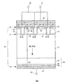
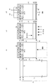
第2番目の不純物濃度ピークの位置は、おもて面から57μmより大きく、60μmより小さい範囲にあってよい。
第3番目の不純物濃度ピークの位置は、おもて面から65μmより大きく、68μmより小さい範囲にあってよい。
プロトン以外の不純物濃度ピークの位置は、おもて面から68μmより大きく、70μmより小さい範囲にあってよい。

Claims (12)
- 第1の面と前記第1の面の反対側に位置する第2の面とを有する第1導電型の半導体層と、
前記第1導電型の半導体層の前記第1の面に接して設けられた第2導電型の半導体層と
を備え、
前記第1導電型の半導体層は、前記第1の面から前記第2の面への第1方向の異なる位置において、複数の不純物濃度ピークを有し、
前記第1方向における前記第1導電型の半導体層と前記第2導電型の半導体層との接合界面である前記第1の面から、前記複数の不純物濃度ピークのうち前記第1の面に1番目に近い第1番目の不純物濃度ピークと、前記第1の面に2番目に近い第2番目の不純物濃度ピークとの境界までにおける積分濃度が、臨界積分濃度以下である、半導体装置。 - 前記第1方向における前記第1の面から、前記第2番目の不純物濃度ピークと、前記複数の不純物濃度ピークのうち前記第1の面に3番目に近い第3番目の不純物濃度ピークとの境界までの積分濃度が、前記臨界積分濃度以下である、
請求項1に記載の半導体装置。 - 前記第1導電型の半導体層は、前記複数の不純物濃度ピークのうち前記第3番目の不純物濃度ピークよりも前記第2の面側に、プロトン以外の不純物濃度ピークを有する
請求項2に記載の半導体装置。 - 前記第1方向における前記第1の面から、前記第3番目の不純物濃度ピークと、前記プロトン以外の不純物濃度ピークとの境界までの積分濃度が、前記臨界積分濃度以下である
請求項3に記載の半導体装置。 - 前記第1方向における前記第1の面から、前記第3番目の不純物濃度ピークまでの積分濃度が、前記臨界積分濃度以下である
請求項3に記載の半導体装置。 - 前記第1導電型の半導体層は、前記第2の面と、前記プロトン以外の不純物の濃度ピークとの間に、前記プロトン以外の不純物の濃度ピークよりも高い不純物濃度の第2導電型の不純物濃度ピークを有する
請求項3に記載の半導体装置。 - 前記第1導電型の半導体層および前記第2導電型の半導体層の前記第1方向における長さに対する前記第2導電型の半導体層の前記接合界面とは反対側に位置するおもて面から、前記第1番目の不純物濃度ピークの位置までの割合は、85%より大きく、89%より小さい範囲であり、
前記第1導電型の半導体層および前記第2導電型の半導体層の前記第1方向における長さに対する前記おもて面から、前記第2番目の不純物濃度ピークの位置までの割合は、89%より大きく、91%より小さい範囲であり、
前記第1導電型の半導体層および前記第2導電型の半導体層の前記第1方向における長さに対する前記おもて面から、前記第3番目の不純物濃度ピークの位置までの割合は、96%より大きく、98%より小さい範囲であり、
前記第1導電型の半導体層および前記第2導電型の半導体層の前記第1方向における長さに対する前記おもて面から、前記プロトン以外の不純物濃度ピークの位置までの割合は、98%より大きく、100%より小さい範囲である
請求項3に記載の半導体装置。 - 前記第1番目の不純物濃度ピークの位置は、前記第2導電型の半導体層の前記接合界面とは反対側に位置するおもて面から94μmより大きく、97μmより小さい範囲にあり、
前記第2番目の不純物濃度ピークの位置は、前記おもて面から97μmより大きく、100μmより小さい範囲にあり、
前記第3番目の不純物濃度ピークの位置は、前記おもて面から105μmより大きく、108μmより小さい範囲にあり、
前記プロトン以外の不純物濃度ピークの位置は、前記おもて面から108μmより大きく、110μmより小さい範囲にある
請求項3に記載の半導体装置。 - 前記第1導電型の半導体層および前記第2導電型の半導体層の前記第1方向における長さに対する前記第2導電型の半導体層の前記接合界面とは反対側に位置するおもて面から、前記第1番目の不純物濃度ピークの位置までの割合は、77%より大きく、81%より小さい範囲であり、
前記第1導電型の半導体層および前記第2導電型の半導体層の前記第1方向における長さに対する前記おもて面から前記第2番目の不純物濃度ピークの位置までの割合は、81%より大きく、86%より小さい範囲であり、
前記第1導電型の半導体層および前記第2導電型の半導体層の前記第1方向における長さに対する前記おもて面から前記第3番目の不純物濃度ピークの位置までの割合は、93%より大きく、97%より小さい範囲であり、
前記第1導電型の半導体層および前記第2導電型の半導体層の前記第1方向における長さに対する前記おもて面から前記プロトン以外の不純物濃度ピークの位置までの割合は、97%より大きく、100%より小さい範囲である、
請求項3に記載の半導体装置。 - 前記第1番目の不純物濃度ピークの位置は、前記第2導電型の半導体層の前記接合界面とは反対側に位置するおもて面から54μmより大きく、57μmより小さい範囲にあり、
前記第2番目の不純物濃度ピークの位置は、前記おもて面から57μmより大きく、60μmより小さい範囲にあり、
前記第3番目の不純物濃度ピークの位置は、前記おもて面から65μmより大きく、68μmより小さい範囲にあり、
前記プロトン以外の不純物濃度ピークの位置は、前記おもて面から68μmより大きく、70μmより小さい範囲にある、
請求項3に記載の半導体装置。 - 少なくとも前記第2導電型の半導体層の一部において、トレンチ状に設けられたゲート絶縁膜と、
前記ゲート絶縁膜に接して設けられたゲート電極と
をさらに有する、請求項1に記載の半導体装置。 - 前記第1番目から第3番目の不純物濃度ピークは、水素、空孔及び酸素による複合ドナーを含むことを特徴とする請求項1に記載の半導体装置。
Applications Claiming Priority (2)
| Application Number | Priority Date | Filing Date | Title |
|---|---|---|---|
| JP2015122037 | 2015-06-17 | ||
| JP2015122037 | 2015-06-17 |
Related Parent Applications (1)
| Application Number | Title | Priority Date | Filing Date |
|---|---|---|---|
| JP2017242421A Division JP6562066B2 (ja) | 2015-06-17 | 2017-12-19 | 半導体装置 |
Publications (2)
| Publication Number | Publication Date |
|---|---|
| JP2019096897A true JP2019096897A (ja) | 2019-06-20 |
| JP6725015B2 JP6725015B2 (ja) | 2020-07-15 |
Family
ID=57545874
Family Applications (3)
| Application Number | Title | Priority Date | Filing Date |
|---|---|---|---|
| JP2017525230A Active JP6292349B2 (ja) | 2015-06-17 | 2016-06-13 | 半導体装置 |
| JP2017242421A Active JP6562066B2 (ja) | 2015-06-17 | 2017-12-19 | 半導体装置 |
| JP2019014714A Active JP6725015B2 (ja) | 2015-06-17 | 2019-01-30 | 半導体装置 |
Family Applications Before (2)
| Application Number | Title | Priority Date | Filing Date |
|---|---|---|---|
| JP2017525230A Active JP6292349B2 (ja) | 2015-06-17 | 2016-06-13 | 半導体装置 |
| JP2017242421A Active JP6562066B2 (ja) | 2015-06-17 | 2017-12-19 | 半導体装置 |
Country Status (5)
| Country | Link |
|---|---|
| US (1) | US10229972B2 (ja) |
| JP (3) | JP6292349B2 (ja) |
| CN (2) | CN107004716B (ja) |
| DE (1) | DE112016000168B4 (ja) |
| WO (1) | WO2016204126A1 (ja) |
Cited By (3)
| Publication number | Priority date | Publication date | Assignee | Title |
|---|---|---|---|---|
| JP2022035046A (ja) * | 2020-08-20 | 2022-03-04 | 三菱電機株式会社 | 半導体装置 |
| JP2022103589A (ja) * | 2020-12-28 | 2022-07-08 | 三菱電機株式会社 | 半導体装置及びその製造方法 |
| WO2022265061A1 (ja) * | 2021-06-17 | 2022-12-22 | 富士電機株式会社 | 半導体装置および半導体装置の製造方法 |
Families Citing this family (24)
| Publication number | Priority date | Publication date | Assignee | Title |
|---|---|---|---|---|
| JP6237921B2 (ja) * | 2014-09-30 | 2017-11-29 | 富士電機株式会社 | 半導体装置および半導体装置の製造方法 |
| JP6820738B2 (ja) * | 2016-12-27 | 2021-01-27 | 三菱電機株式会社 | 半導体装置、電力変換装置および半導体装置の製造方法 |
| WO2018135448A1 (ja) | 2017-01-17 | 2018-07-26 | 富士電機株式会社 | 半導体装置 |
| DE102017126853B4 (de) * | 2017-11-15 | 2019-11-21 | Infineon Technologies Dresden Gmbh | Halbleitervorrichtung mit Puffergebiet |
| DE212019000150U1 (de) | 2018-08-10 | 2020-07-29 | Rohm Co., Ltd. | SiC-Halbleiterbauteil |
| JP6664446B2 (ja) * | 2018-08-10 | 2020-03-13 | ローム株式会社 | SiC半導体装置 |
| JP6964566B2 (ja) * | 2018-08-17 | 2021-11-10 | 三菱電機株式会社 | 半導体装置およびその製造方法 |
| JP6993946B2 (ja) * | 2018-08-21 | 2022-01-14 | 株式会社東芝 | 半導体素子 |
| JP7010184B2 (ja) * | 2018-09-13 | 2022-01-26 | 株式会社デンソー | 半導体装置 |
| DE102018132236B4 (de) | 2018-12-14 | 2023-04-27 | Infineon Technologies Ag | Leistungshalbleiterbauelement und Verfahren zu dessen Herstellung |
| JP7375340B2 (ja) * | 2019-06-12 | 2023-11-08 | サンケン電気株式会社 | 半導体装置 |
| WO2021029285A1 (ja) | 2019-08-09 | 2021-02-18 | 富士電機株式会社 | 半導体装置 |
| WO2021075330A1 (ja) * | 2019-10-17 | 2021-04-22 | 富士電機株式会社 | 半導体装置および半導体装置の製造方法 |
| JP7129437B2 (ja) * | 2020-02-17 | 2022-09-01 | ローム株式会社 | SiC半導体装置 |
| DE112021000082T5 (de) | 2020-03-04 | 2022-04-21 | Fuji Electric Co., Ltd. | Halbleitervorrichtung, verfahren zur herstellung einer halbleitervorrichtung und leistungsumwandlungsvorrichtung mit einer halbleitervorrichtung |
| CN113471273A (zh) * | 2020-03-31 | 2021-10-01 | 比亚迪半导体股份有限公司 | 绝缘栅双极型晶体管及制备方法、电子设备 |
| DE112021000205T5 (de) * | 2020-07-15 | 2022-08-18 | Fuji Electric Co., Ltd. | Halbleitervorrichtung |
| JP7528628B2 (ja) * | 2020-08-20 | 2024-08-06 | 三菱電機株式会社 | 半導体装置および半導体装置の製造方法 |
| WO2022107727A1 (ja) | 2020-11-17 | 2022-05-27 | 富士電機株式会社 | 半導体装置 |
| CN116978937A (zh) * | 2021-02-07 | 2023-10-31 | 华为技术有限公司 | 半导体器件及相关模块、电路、制备方法 |
| CN113644123B (zh) * | 2021-06-28 | 2024-09-06 | 华为技术有限公司 | 半导体器件及相关芯片和制备方法 |
| JP7597233B2 (ja) * | 2021-09-15 | 2024-12-10 | 富士電機株式会社 | 半導体装置および半導体装置の製造方法 |
| JP7852281B2 (ja) | 2022-02-17 | 2026-04-28 | 富士電機株式会社 | 半導体装置 |
| JP7845142B2 (ja) * | 2022-10-27 | 2026-04-14 | 株式会社デンソー | 半導体装置 |
Citations (4)
| Publication number | Priority date | Publication date | Assignee | Title |
|---|---|---|---|---|
| US20060081923A1 (en) * | 2004-09-30 | 2006-04-20 | Infineon Technologies Ag | Semiconductor device and fabrication method suitable therefor |
| US20080001257A1 (en) * | 2006-06-30 | 2008-01-03 | Infineon Technologies Austria Ag | Semiconductor device with a field stop zone |
| WO2011052787A1 (ja) * | 2009-11-02 | 2011-05-05 | 富士電機システムズ株式会社 | 半導体装置および半導体装置の製造方法 |
| WO2013073623A1 (ja) * | 2011-11-15 | 2013-05-23 | 富士電機株式会社 | 半導体装置および半導体装置の製造方法 |
Family Cites Families (12)
| Publication number | Priority date | Publication date | Assignee | Title |
|---|---|---|---|---|
| US6482681B1 (en) * | 2000-05-05 | 2002-11-19 | International Rectifier Corporation | Hydrogen implant for buffer zone of punch-through non epi IGBT |
| JP4093042B2 (ja) * | 2002-12-09 | 2008-05-28 | 富士電機デバイステクノロジー株式会社 | 半導体装置 |
| JP2006049473A (ja) * | 2004-08-03 | 2006-02-16 | Toyota Central Res & Dev Lab Inc | 縦型半導体装置 |
| US7989888B2 (en) * | 2006-08-31 | 2011-08-02 | Infineon Technologies Autria AG | Semiconductor device with a field stop zone and process of producing the same |
| EP2045844A1 (en) | 2007-10-03 | 2009-04-08 | ABB Technology AG | Semiconductor Module |
| US7960222B1 (en) * | 2007-11-21 | 2011-06-14 | National Semiconductor Corporation | System and method for manufacturing double EPI N-type lateral diffusion metal oxide semiconductor transistors |
| JP5365009B2 (ja) | 2008-01-23 | 2013-12-11 | 富士電機株式会社 | 半導体装置およびその製造方法 |
| JP6006918B2 (ja) * | 2011-06-06 | 2016-10-12 | ルネサスエレクトロニクス株式会社 | 半導体装置、半導体装置の製造方法、及び電子装置 |
| JP5817686B2 (ja) * | 2011-11-30 | 2015-11-18 | 株式会社デンソー | 半導体装置 |
| WO2013089256A1 (ja) * | 2011-12-15 | 2013-06-20 | 富士電機株式会社 | 半導体装置および半導体装置の製造方法 |
| EP2790209B1 (en) * | 2012-03-30 | 2019-09-25 | Fuji Electric Co., Ltd. | Manufacturing method for semiconductor device |
| KR102070959B1 (ko) * | 2012-04-24 | 2020-01-30 | 온세미컨덕터코리아 주식회사 | 파워 소자 및 그 제조방법 |
-
2016
- 2016-06-13 CN CN201680003832.6A patent/CN107004716B/zh active Active
- 2016-06-13 CN CN202011371539.XA patent/CN112490281B/zh active Active
- 2016-06-13 JP JP2017525230A patent/JP6292349B2/ja active Active
- 2016-06-13 WO PCT/JP2016/067597 patent/WO2016204126A1/ja not_active Ceased
- 2016-06-13 DE DE112016000168.1T patent/DE112016000168B4/de active Active
-
2017
- 2017-05-30 US US15/607,697 patent/US10229972B2/en active Active
- 2017-12-19 JP JP2017242421A patent/JP6562066B2/ja active Active
-
2019
- 2019-01-30 JP JP2019014714A patent/JP6725015B2/ja active Active
Patent Citations (4)
| Publication number | Priority date | Publication date | Assignee | Title |
|---|---|---|---|---|
| US20060081923A1 (en) * | 2004-09-30 | 2006-04-20 | Infineon Technologies Ag | Semiconductor device and fabrication method suitable therefor |
| US20080001257A1 (en) * | 2006-06-30 | 2008-01-03 | Infineon Technologies Austria Ag | Semiconductor device with a field stop zone |
| WO2011052787A1 (ja) * | 2009-11-02 | 2011-05-05 | 富士電機システムズ株式会社 | 半導体装置および半導体装置の製造方法 |
| WO2013073623A1 (ja) * | 2011-11-15 | 2013-05-23 | 富士電機株式会社 | 半導体装置および半導体装置の製造方法 |
Cited By (7)
| Publication number | Priority date | Publication date | Assignee | Title |
|---|---|---|---|---|
| JP2022035046A (ja) * | 2020-08-20 | 2022-03-04 | 三菱電機株式会社 | 半導体装置 |
| JP7374054B2 (ja) | 2020-08-20 | 2023-11-06 | 三菱電機株式会社 | 半導体装置 |
| JP2022103589A (ja) * | 2020-12-28 | 2022-07-08 | 三菱電機株式会社 | 半導体装置及びその製造方法 |
| JP7415913B2 (ja) | 2020-12-28 | 2024-01-17 | 三菱電機株式会社 | 半導体装置及びその製造方法 |
| WO2022265061A1 (ja) * | 2021-06-17 | 2022-12-22 | 富士電機株式会社 | 半導体装置および半導体装置の製造方法 |
| JPWO2022265061A1 (ja) * | 2021-06-17 | 2022-12-22 | ||
| JP7670132B2 (ja) | 2021-06-17 | 2025-04-30 | 富士電機株式会社 | 半導体装置および半導体装置の製造方法 |
Also Published As
| Publication number | Publication date |
|---|---|
| CN112490281A (zh) | 2021-03-12 |
| DE112016000168T5 (de) | 2017-08-03 |
| CN107004716B (zh) | 2020-12-18 |
| US20170278929A1 (en) | 2017-09-28 |
| JP6292349B2 (ja) | 2018-03-14 |
| DE112016000168B4 (de) | 2025-02-20 |
| WO2016204126A1 (ja) | 2016-12-22 |
| JP2018082191A (ja) | 2018-05-24 |
| JPWO2016204126A1 (ja) | 2017-09-14 |
| CN107004716A (zh) | 2017-08-01 |
| JP6562066B2 (ja) | 2019-08-21 |
| CN112490281B (zh) | 2025-02-25 |
| JP6725015B2 (ja) | 2020-07-15 |
| US10229972B2 (en) | 2019-03-12 |
Similar Documents
| Publication | Publication Date | Title |
|---|---|---|
| JP2019096897A (ja) | 半導体装置 | |
| JP7655354B2 (ja) | 半導体装置および半導体装置の製造方法 | |
| US10497801B2 (en) | Method of manufacturing a semiconductor device having an undulated profile of net doping in a drift zone | |
| CN109075213B (zh) | 半导体装置 | |
| CN101908558B (zh) | 半导体装置 | |
| CN103986447B (zh) | 双极半导体开关及其制造方法 | |
| CN110034173B (zh) | 宽带隙半导体器件和形成宽带隙半导体器件的方法 | |
| CN104299991B (zh) | 半导体装置 | |
| JP2019102493A (ja) | 炭化珪素半導体装置および炭化珪素半導体装置の製造方法 | |
| JP7582733B2 (ja) | 炭化珪素からなるトレンチゲート構造の縦型mosfet | |
| US20160027867A1 (en) | Semiconductor device | |
| US20200273970A1 (en) | Semiconductor device | |
| CN103383957A (zh) | 一种逆导型igbt器件 | |
| CN114078962A (zh) | 半导体装置 | |
| WO2023042886A1 (ja) | 半導体装置および半導体装置の製造方法 | |
| WO2018154963A1 (ja) | 半導体装置 | |
| JP7670132B2 (ja) | 半導体装置および半導体装置の製造方法 | |
| JP6930113B2 (ja) | 半導体装置および半導体装置の製造方法 | |
| CN104465792A (zh) | 半导体装置 | |
| JP7276407B2 (ja) | 炭化珪素半導体装置 | |
| Donlon et al. | Chip improvements for future IGBT modules | |
| JP2024100692A (ja) | 半導体装置 | |
| CN118352354A (zh) | 半导体装置 |
Legal Events
| Date | Code | Title | Description |
|---|---|---|---|
| A521 | Request for written amendment filed |
Free format text: JAPANESE INTERMEDIATE CODE: A523 Effective date: 20190130 |
|
| A621 | Written request for application examination |
Free format text: JAPANESE INTERMEDIATE CODE: A621 Effective date: 20190130 |
|
| A977 | Report on retrieval |
Free format text: JAPANESE INTERMEDIATE CODE: A971007 Effective date: 20191031 |
|
| A131 | Notification of reasons for refusal |
Free format text: JAPANESE INTERMEDIATE CODE: A131 Effective date: 20191112 |
|
| A521 | Request for written amendment filed |
Free format text: JAPANESE INTERMEDIATE CODE: A523 Effective date: 20200109 |
|
| TRDD | Decision of grant or rejection written | ||
| A01 | Written decision to grant a patent or to grant a registration (utility model) |
Free format text: JAPANESE INTERMEDIATE CODE: A01 Effective date: 20200526 |
|
| A61 | First payment of annual fees (during grant procedure) |
Free format text: JAPANESE INTERMEDIATE CODE: A61 Effective date: 20200608 |
|
| R150 | Certificate of patent or registration of utility model |
Ref document number: 6725015 Country of ref document: JP Free format text: JAPANESE INTERMEDIATE CODE: R150 |
|
| R250 | Receipt of annual fees |
Free format text: JAPANESE INTERMEDIATE CODE: R250 |
|
| R250 | Receipt of annual fees |
Free format text: JAPANESE INTERMEDIATE CODE: R250 |
|
| R250 | Receipt of annual fees |
Free format text: JAPANESE INTERMEDIATE CODE: R250 |