JP3639302B2 - 樹脂封止型半導体装置 - Google Patents
樹脂封止型半導体装置 Download PDFInfo
- Publication number
- JP3639302B2 JP3639302B2 JP2004240416A JP2004240416A JP3639302B2 JP 3639302 B2 JP3639302 B2 JP 3639302B2 JP 2004240416 A JP2004240416 A JP 2004240416A JP 2004240416 A JP2004240416 A JP 2004240416A JP 3639302 B2 JP3639302 B2 JP 3639302B2
- Authority
- JP
- Japan
- Prior art keywords
- semiconductor device
- lead
- resin
- die pad
- sealing resin
- Prior art date
- Legal status (The legal status is an assumption and is not a legal conclusion. Google has not performed a legal analysis and makes no representation as to the accuracy of the status listed.)
- Expired - Lifetime
Links
Images




Classifications
-
- H—ELECTRICITY
- H10—SEMICONDUCTOR DEVICES; ELECTRIC SOLID-STATE DEVICES NOT OTHERWISE PROVIDED FOR
- H10W—GENERIC PACKAGES, INTERCONNECTIONS, CONNECTORS OR OTHER CONSTRUCTIONAL DETAILS OF DEVICES COVERED BY CLASS H10
- H10W90/00—Package configurations
- H10W90/701—Package configurations characterised by the relative positions of pads or connectors relative to package parts
- H10W90/751—Package configurations characterised by the relative positions of pads or connectors relative to package parts of bond wires
- H10W90/756—Package configurations characterised by the relative positions of pads or connectors relative to package parts of bond wires between a chip and a stacked lead frame, conducting package substrate or heat sink
Landscapes
- Lead Frames For Integrated Circuits (AREA)
Description
図1,図2及び図3は、それぞれ本発明の第1の実施形態に係る樹脂封止型半導体装置の構造を説明する断面図,上面図及び裏面図である。ただし、図2の平面図では、内部構造を理解しやすくするため、封止樹脂を透視した状態を示している。また、図1は、図2に示すI-I線における断面図である。
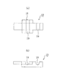
次に、第2の実施形態について説明する。図5は本実施形態における半導体装置の裏面図である。本実施形態においても、半導体装置の断面構造は上記第1の実施形態における図1に示す構造と同じであるので、断面図の図示は省略する。また、本実施形態の半導体装置の上面構造は図5に示す裏面図から容易に理解できるので、上面図の図示は省略する。
次に、第3の実施形態について説明する。図6は本実施形態における半導体装置の裏面図である。本実施形態においても、半導体装置の断面構造は上記第1の実施形態における図1に示す構造と同じであるので、断面図の図示は省略する。また、本実施形態の半導体装置の上面構造は図6に示す裏面図から容易に理解できるので、上面図の図示は省略する。
次に、上記各実施形態に共通に適用できる他の実施形態について説明する。
12 半導体チップ
13 リード
14 金属細線(接続部材)
15 封止樹脂
16 外部電極
17 段差部
18 幅広部
19 溝
20 外枠
Claims (9)
- ダイパッドと、
溝を有するリードと、
前記ダイパッドに搭載された半導体チップと、
前記半導体チップと前記リードとを電気的に接続する金属細線と、
前記溝と、前記金属細線と、前記半導体チップと、前記リードの上面とを封止し、かつ、前記リードの下面の一部を露出する封止樹脂とを備え、
前記溝は、前記リードの下面の露出部の上方に位置し、
前記リードは、上方の幅が下方の幅よりも広い部分を有し、
前記金属細線は、前記リードの前記溝の上でない部分であって、前記封止樹脂に封止された部分に接続される樹脂封止型半導体装置。 - 前記リードの下面の一部以外の部分が前記封止樹脂により封止された請求項1に記載の樹脂封止型半導体装置。
- 前記リードは、上面が下面よりも大きい請求項1又は2に記載の樹脂封止型半導体装置。
- 前記溝は、前記リードの上面に形成されている請求項1から3のいずれかに記載の樹脂封止型半導体装置。
- 前記リードは、前記溝よりも前記ダイパッド側に薄肉部を有し、前記薄肉部の厚みは、前記リードの下面の露出部と前記リードの前記溝を除く上面とで構成される厚みよりも薄い請求項1から4のいずれかに記載の樹脂封止型半導体装置。
- 前記薄肉部の下方に前記樹脂封止を有している請求項5に記載の樹脂封止型半導体装置。
- 前記半導体チップは、前記ダイパッドからはみ出して搭載されている請求項1から6のいずれかに記載の樹脂封止型半導体装置。
- 前記封止樹脂は、前記ダイパッドの下面を露出している請求項1から7のいずれかに記載の樹脂封止型半導体装置。
- 前記封止樹脂の側面と前記リードの先端とがほぼ同一面である請求項1から8のいずれかに記載の樹脂封止型半導体装置。
Priority Applications (1)
| Application Number | Priority Date | Filing Date | Title |
|---|---|---|---|
| JP2004240416A JP3639302B2 (ja) | 2004-08-20 | 2004-08-20 | 樹脂封止型半導体装置 |
Applications Claiming Priority (1)
| Application Number | Priority Date | Filing Date | Title |
|---|---|---|---|
| JP2004240416A JP3639302B2 (ja) | 2004-08-20 | 2004-08-20 | 樹脂封止型半導体装置 |
Related Parent Applications (1)
| Application Number | Title | Priority Date | Filing Date |
|---|---|---|---|
| JP10016498A Division JPH11214606A (ja) | 1998-01-29 | 1998-01-29 | 樹脂封止型半導体装置及びリードフレーム |
Publications (2)
| Publication Number | Publication Date |
|---|---|
| JP2004328015A JP2004328015A (ja) | 2004-11-18 |
| JP3639302B2 true JP3639302B2 (ja) | 2005-04-20 |
Family
ID=33509492
Family Applications (1)
| Application Number | Title | Priority Date | Filing Date |
|---|---|---|---|
| JP2004240416A Expired - Lifetime JP3639302B2 (ja) | 2004-08-20 | 2004-08-20 | 樹脂封止型半導体装置 |
Country Status (1)
| Country | Link |
|---|---|
| JP (1) | JP3639302B2 (ja) |
Families Citing this family (5)
| Publication number | Priority date | Publication date | Assignee | Title |
|---|---|---|---|---|
| JP5183572B2 (ja) * | 2009-06-08 | 2013-04-17 | 株式会社三井ハイテック | リードフレーム及び半導体装置 |
| JP5255009B2 (ja) | 2010-02-26 | 2013-08-07 | ルネサスエレクトロニクス株式会社 | 半導体装置 |
| JP6253531B2 (ja) | 2014-06-30 | 2017-12-27 | ルネサスエレクトロニクス株式会社 | 半導体装置 |
| CN111602240B (zh) * | 2018-03-02 | 2023-08-01 | 新电元工业株式会社 | 树脂封装型半导体装置 |
| CN116613132A (zh) * | 2023-07-19 | 2023-08-18 | 青岛泰睿思微电子有限公司 | 射频类的芯片封装结构及方法 |
-
2004
- 2004-08-20 JP JP2004240416A patent/JP3639302B2/ja not_active Expired - Lifetime
Also Published As
| Publication number | Publication date |
|---|---|
| JP2004328015A (ja) | 2004-11-18 |
Similar Documents
| Publication | Publication Date | Title |
|---|---|---|
| CN100414696C (zh) | 引线框及制造方法以及树脂密封型半导体器件及制造方法 | |
| US9171761B2 (en) | Resin sealing type semiconductor device and method of manufacturing the same, and lead frame | |
| US6753599B2 (en) | Semiconductor package and mounting structure on substrate thereof and stack structure thereof | |
| JP2000188366A (ja) | 半導体装置 | |
| US20090020859A1 (en) | Quad flat package with exposed common electrode bars | |
| JP2000307045A (ja) | リードフレームおよびそれを用いた樹脂封止型半導体装置の製造方法 | |
| JP3470111B2 (ja) | 樹脂封止型半導体装置の製造方法 | |
| JPH11214606A (ja) | 樹脂封止型半導体装置及びリードフレーム | |
| JP4091050B2 (ja) | 半導体装置の製造方法 | |
| JP2000091488A (ja) | 樹脂封止型半導体装置とそれに用いられる回路部材 | |
| CN101325190A (zh) | 导线架上具有图案的四方扁平无引脚封装结构 | |
| JP3639302B2 (ja) | 樹脂封止型半導体装置 | |
| JP2569400B2 (ja) | 樹脂封止型半導体装置の製造方法 | |
| JP3502377B2 (ja) | リードフレーム、樹脂封止型半導体装置及びその製造方法 | |
| JPH10275887A (ja) | 半導体装置 | |
| JP6923299B2 (ja) | 半導体装置及び半導体装置の製造方法 | |
| JPH09116045A (ja) | リードフレームを用いたbgaタイプの樹脂封止型半導体装置およびその製造方法 | |
| JPH11233709A (ja) | 半導体装置およびその製造方法ならびに電子装置 | |
| JP2001077285A (ja) | リードフレームとそれを用いた樹脂封止型半導体装置の製造方法 | |
| KR100668932B1 (ko) | 리드프레임 및 이를 이용한 반도체패키지 | |
| JP3361917B2 (ja) | リードフレーム、半導体装置および半導体装置の製造方法 | |
| JP2004200719A (ja) | 半導体装置 | |
| JP2003007954A (ja) | 樹脂封止型半導体装置の製造方法 | |
| KR200159861Y1 (ko) | 반도체 패키지 | |
| JPH1126643A (ja) | 半導体装置 |
Legal Events
| Date | Code | Title | Description |
|---|---|---|---|
| A521 | Request for written amendment filed |
Free format text: JAPANESE INTERMEDIATE CODE: A523 Effective date: 20040826 |
|
| A621 | Written request for application examination |
Free format text: JAPANESE INTERMEDIATE CODE: A621 Effective date: 20040826 |
|
| A871 | Explanation of circumstances concerning accelerated examination |
Free format text: JAPANESE INTERMEDIATE CODE: A871 Effective date: 20040826 |
|
| A975 | Report on accelerated examination |
Free format text: JAPANESE INTERMEDIATE CODE: A971005 Effective date: 20040922 |
|
| A131 | Notification of reasons for refusal |
Free format text: JAPANESE INTERMEDIATE CODE: A131 Effective date: 20041005 |
|
| A521 | Request for written amendment filed |
Free format text: JAPANESE INTERMEDIATE CODE: A523 Effective date: 20041206 |
|
| TRDD | Decision of grant or rejection written | ||
| A01 | Written decision to grant a patent or to grant a registration (utility model) |
Free format text: JAPANESE INTERMEDIATE CODE: A01 Effective date: 20050105 |
|
| A61 | First payment of annual fees (during grant procedure) |
Free format text: JAPANESE INTERMEDIATE CODE: A61 Effective date: 20050113 |
|
| R150 | Certificate of patent or registration of utility model |
Free format text: JAPANESE INTERMEDIATE CODE: R150 |
|
| FPAY | Renewal fee payment (event date is renewal date of database) |
Free format text: PAYMENT UNTIL: 20080121 Year of fee payment: 3 |
|
| FPAY | Renewal fee payment (event date is renewal date of database) |
Free format text: PAYMENT UNTIL: 20090121 Year of fee payment: 4 |
|
| FPAY | Renewal fee payment (event date is renewal date of database) |
Free format text: PAYMENT UNTIL: 20090121 Year of fee payment: 4 |
|
| FPAY | Renewal fee payment (event date is renewal date of database) |
Free format text: PAYMENT UNTIL: 20100121 Year of fee payment: 5 |
|
| FPAY | Renewal fee payment (event date is renewal date of database) |
Free format text: PAYMENT UNTIL: 20110121 Year of fee payment: 6 |
|
| FPAY | Renewal fee payment (event date is renewal date of database) |
Free format text: PAYMENT UNTIL: 20110121 Year of fee payment: 6 |
|
| FPAY | Renewal fee payment (event date is renewal date of database) |
Free format text: PAYMENT UNTIL: 20120121 Year of fee payment: 7 |
|
| FPAY | Renewal fee payment (event date is renewal date of database) |
Free format text: PAYMENT UNTIL: 20130121 Year of fee payment: 8 |
|
| FPAY | Renewal fee payment (event date is renewal date of database) |
Free format text: PAYMENT UNTIL: 20130121 Year of fee payment: 8 |
|
| EXPY | Cancellation because of completion of term |