JP3836697B2 - 半導体素子 - Google Patents
半導体素子 Download PDFInfo
- Publication number
- JP3836697B2 JP3836697B2 JP2001267299A JP2001267299A JP3836697B2 JP 3836697 B2 JP3836697 B2 JP 3836697B2 JP 2001267299 A JP2001267299 A JP 2001267299A JP 2001267299 A JP2001267299 A JP 2001267299A JP 3836697 B2 JP3836697 B2 JP 3836697B2
- Authority
- JP
- Japan
- Prior art keywords
- less
- conductive layer
- semiconductor element
- dislocation density
- epitaxially grown
- Prior art date
- Legal status (The legal status is an assumption and is not a legal conclusion. Google has not performed a legal analysis and makes no representation as to the accuracy of the status listed.)
- Expired - Lifetime
Links
Images
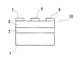


Classifications
-
- H—ELECTRICITY
- H10—SEMICONDUCTOR DEVICES; ELECTRIC SOLID-STATE DEVICES NOT OTHERWISE PROVIDED FOR
- H10D—INORGANIC ELECTRIC SEMICONDUCTOR DEVICES
- H10D10/00—Bipolar junction transistors [BJT]
- H10D10/01—Manufacture or treatment
- H10D10/021—Manufacture or treatment of heterojunction BJTs [HBT]
-
- H—ELECTRICITY
- H10—SEMICONDUCTOR DEVICES; ELECTRIC SOLID-STATE DEVICES NOT OTHERWISE PROVIDED FOR
- H10D—INORGANIC ELECTRIC SEMICONDUCTOR DEVICES
- H10D30/00—Field-effect transistors [FET]
- H10D30/01—Manufacture or treatment
- H10D30/015—Manufacture or treatment of FETs having heterojunction interface channels or heterojunction gate electrodes, e.g. HEMT
-
- H—ELECTRICITY
- H10—SEMICONDUCTOR DEVICES; ELECTRIC SOLID-STATE DEVICES NOT OTHERWISE PROVIDED FOR
- H10D—INORGANIC ELECTRIC SEMICONDUCTOR DEVICES
- H10D30/00—Field-effect transistors [FET]
- H10D30/01—Manufacture or treatment
- H10D30/061—Manufacture or treatment of FETs having Schottky gates
-
- H—ELECTRICITY
- H10—SEMICONDUCTOR DEVICES; ELECTRIC SOLID-STATE DEVICES NOT OTHERWISE PROVIDED FOR
- H10D—INORGANIC ELECTRIC SEMICONDUCTOR DEVICES
- H10D30/00—Field-effect transistors [FET]
- H10D30/01—Manufacture or treatment
- H10D30/061—Manufacture or treatment of FETs having Schottky gates
- H10D30/0612—Manufacture or treatment of FETs having Schottky gates of lateral single-gate Schottky FETs
- H10D30/0614—Manufacture or treatment of FETs having Schottky gates of lateral single-gate Schottky FETs using processes wherein the final gate is made after the completion of the source and drain regions, e.g. gate-last processes using dummy gates
-
- H—ELECTRICITY
- H10—SEMICONDUCTOR DEVICES; ELECTRIC SOLID-STATE DEVICES NOT OTHERWISE PROVIDED FOR
- H10P—GENERIC PROCESSES OR APPARATUS FOR THE MANUFACTURE OR TREATMENT OF DEVICES COVERED BY CLASS H10
- H10P14/00—Formation of materials, e.g. in the shape of layers or pillars
- H10P14/20—Formation of materials, e.g. in the shape of layers or pillars of semiconductor materials
- H10P14/24—Formation of materials, e.g. in the shape of layers or pillars of semiconductor materials using chemical vapour deposition [CVD]
-
- H—ELECTRICITY
- H10—SEMICONDUCTOR DEVICES; ELECTRIC SOLID-STATE DEVICES NOT OTHERWISE PROVIDED FOR
- H10P—GENERIC PROCESSES OR APPARATUS FOR THE MANUFACTURE OR TREATMENT OF DEVICES COVERED BY CLASS H10
- H10P14/00—Formation of materials, e.g. in the shape of layers or pillars
- H10P14/20—Formation of materials, e.g. in the shape of layers or pillars of semiconductor materials
- H10P14/29—Formation of materials, e.g. in the shape of layers or pillars of semiconductor materials characterised by the substrates
- H10P14/2901—Materials
-
- H—ELECTRICITY
- H10—SEMICONDUCTOR DEVICES; ELECTRIC SOLID-STATE DEVICES NOT OTHERWISE PROVIDED FOR
- H10P—GENERIC PROCESSES OR APPARATUS FOR THE MANUFACTURE OR TREATMENT OF DEVICES COVERED BY CLASS H10
- H10P14/00—Formation of materials, e.g. in the shape of layers or pillars
- H10P14/20—Formation of materials, e.g. in the shape of layers or pillars of semiconductor materials
- H10P14/29—Formation of materials, e.g. in the shape of layers or pillars of semiconductor materials characterised by the substrates
- H10P14/2901—Materials
- H10P14/2921—Materials being crystalline insulating materials
-
- H—ELECTRICITY
- H10—SEMICONDUCTOR DEVICES; ELECTRIC SOLID-STATE DEVICES NOT OTHERWISE PROVIDED FOR
- H10P—GENERIC PROCESSES OR APPARATUS FOR THE MANUFACTURE OR TREATMENT OF DEVICES COVERED BY CLASS H10
- H10P14/00—Formation of materials, e.g. in the shape of layers or pillars
- H10P14/20—Formation of materials, e.g. in the shape of layers or pillars of semiconductor materials
- H10P14/32—Formation of materials, e.g. in the shape of layers or pillars of semiconductor materials characterised by intermediate layers between substrates and deposited layers
- H10P14/3202—Materials thereof
- H10P14/3214—Materials thereof being Group IIIA-VA semiconductors
- H10P14/3216—Nitrides
-
- H—ELECTRICITY
- H10—SEMICONDUCTOR DEVICES; ELECTRIC SOLID-STATE DEVICES NOT OTHERWISE PROVIDED FOR
- H10P—GENERIC PROCESSES OR APPARATUS FOR THE MANUFACTURE OR TREATMENT OF DEVICES COVERED BY CLASS H10
- H10P14/00—Formation of materials, e.g. in the shape of layers or pillars
- H10P14/20—Formation of materials, e.g. in the shape of layers or pillars of semiconductor materials
- H10P14/34—Deposited materials, e.g. layers
- H10P14/3402—Deposited materials, e.g. layers characterised by the chemical composition
- H10P14/3414—Deposited materials, e.g. layers characterised by the chemical composition being group IIIA-VIA materials
- H10P14/3416—Nitrides
-
- H—ELECTRICITY
- H10—SEMICONDUCTOR DEVICES; ELECTRIC SOLID-STATE DEVICES NOT OTHERWISE PROVIDED FOR
- H10D—INORGANIC ELECTRIC SEMICONDUCTOR DEVICES
- H10D62/00—Semiconductor bodies, or regions thereof, of devices having potential barriers
- H10D62/80—Semiconductor bodies, or regions thereof, of devices having potential barriers characterised by the materials
- H10D62/85—Semiconductor bodies, or regions thereof, of devices having potential barriers characterised by the materials being Group III-V materials, e.g. GaAs
- H10D62/8503—Nitride Group III-V materials, e.g. AlN or GaN
Landscapes
- Junction Field-Effect Transistors (AREA)
- Chemical Vapour Deposition (AREA)
- Bipolar Transistors (AREA)
- Crystals, And After-Treatments Of Crystals (AREA)
Priority Applications (5)
| Application Number | Priority Date | Filing Date | Title |
|---|---|---|---|
| JP2001267299A JP3836697B2 (ja) | 2000-12-07 | 2001-09-04 | 半導体素子 |
| US10/007,099 US6583468B2 (en) | 2000-12-07 | 2001-12-04 | Semiconductor element |
| EP01128995A EP1213767A3 (fr) | 2000-12-07 | 2001-12-06 | Elément semi-conducteur en composé de nitrure |
| US10/370,350 US6707076B2 (en) | 2000-12-07 | 2003-02-18 | Semiconductor element |
| US10/690,290 US6781164B2 (en) | 2000-12-07 | 2003-10-21 | Semiconductor element |
Applications Claiming Priority (5)
| Application Number | Priority Date | Filing Date | Title |
|---|---|---|---|
| JP2000373039 | 2000-12-07 | ||
| JP2000-373039 | 2000-12-07 | ||
| JP2001-153693 | 2001-05-23 | ||
| JP2001153693 | 2001-05-23 | ||
| JP2001267299A JP3836697B2 (ja) | 2000-12-07 | 2001-09-04 | 半導体素子 |
Related Child Applications (1)
| Application Number | Title | Priority Date | Filing Date |
|---|---|---|---|
| JP2005015790A Division JP2005167275A (ja) | 2000-12-07 | 2005-01-24 | 半導体素子 |
Publications (2)
| Publication Number | Publication Date |
|---|---|
| JP2003045899A JP2003045899A (ja) | 2003-02-14 |
| JP3836697B2 true JP3836697B2 (ja) | 2006-10-25 |
Family
ID=27345391
Family Applications (1)
| Application Number | Title | Priority Date | Filing Date |
|---|---|---|---|
| JP2001267299A Expired - Lifetime JP3836697B2 (ja) | 2000-12-07 | 2001-09-04 | 半導体素子 |
Country Status (3)
| Country | Link |
|---|---|
| US (3) | US6583468B2 (fr) |
| EP (1) | EP1213767A3 (fr) |
| JP (1) | JP3836697B2 (fr) |
Cited By (1)
| Publication number | Priority date | Publication date | Assignee | Title |
|---|---|---|---|---|
| CN104779280A (zh) * | 2014-01-09 | 2015-07-15 | 日立金属株式会社 | 氮化物半导体外延晶圆和氮化物半导体器件 |
Families Citing this family (39)
| Publication number | Priority date | Publication date | Assignee | Title |
|---|---|---|---|---|
| JP4327339B2 (ja) * | 2000-07-28 | 2009-09-09 | 独立行政法人物質・材料研究機構 | 半導体層形成用基板とそれを利用した半導体装置 |
| JP3886341B2 (ja) * | 2001-05-21 | 2007-02-28 | 日本電気株式会社 | 窒化ガリウム結晶基板の製造方法及び窒化ガリウム結晶基板 |
| JP3946969B2 (ja) * | 2001-05-31 | 2007-07-18 | 日本碍子株式会社 | 電界効果トランジスタ、及びヘテロ接合型バイポーラトランジスタ |
| JP3954335B2 (ja) * | 2001-06-15 | 2007-08-08 | 日本碍子株式会社 | Iii族窒化物多層膜 |
| JP4514727B2 (ja) * | 2001-12-25 | 2010-07-28 | 日本碍子株式会社 | Iii族窒化物膜の製造方法、iii族窒化物膜、iii族窒化物素子用エピタキシャル基板、及びiii族窒化物素子 |
| KR100484486B1 (ko) * | 2002-10-18 | 2005-04-20 | 한국전자통신연구원 | 질화물 반도체 전계 효과 트랜지스터 및 그 제조방법 |
| JP4823466B2 (ja) * | 2002-12-18 | 2011-11-24 | 日本碍子株式会社 | エピタキシャル成長用基板および半導体素子 |
| JP2004289005A (ja) * | 2003-03-24 | 2004-10-14 | Ngk Insulators Ltd | エピタキシャル基板、半導体素子および高電子移動度トランジスタ |
| FR2853141A1 (fr) * | 2003-03-26 | 2004-10-01 | Kyocera Corp | Appareil a semi-conducteur, procede pour faire croitre un semi-conducteur a nitrure et procede de production d'un appareil a semi-conducteur |
| JP2004327882A (ja) * | 2003-04-28 | 2004-11-18 | Ngk Insulators Ltd | エピタキシャル基板、半導体素子および高電子移動度トランジスタ |
| US7078743B2 (en) * | 2003-05-15 | 2006-07-18 | Matsushita Electric Industrial Co., Ltd. | Field effect transistor semiconductor device |
| JP2005136200A (ja) * | 2003-10-30 | 2005-05-26 | Univ Nagoya | 窒化物半導体結晶層の作製方法、窒化物半導体結晶層、及び窒化物半導体結晶層作製用の基材 |
| US7238970B2 (en) * | 2003-10-30 | 2007-07-03 | Matsushita Electric Industrial Co., Ltd. | Semiconductor device and method for fabricating the same |
| US6987300B2 (en) * | 2004-03-25 | 2006-01-17 | Microchip Technology Incorporated | High voltage ESD-protection structure |
| US7981744B2 (en) | 2004-06-10 | 2011-07-19 | Toyoda Gosei Co., Ltd. | Field-effect transistor, semiconductor device, a method for manufacturing them, and a method of semiconductor crystal growth |
| JP2006032911A (ja) * | 2004-06-15 | 2006-02-02 | Ngk Insulators Ltd | 半導体積層構造、半導体素子およびhemt素子 |
| JP4712450B2 (ja) * | 2004-06-29 | 2011-06-29 | 日本碍子株式会社 | AlN結晶の表面平坦性改善方法 |
| US7339255B2 (en) * | 2004-08-24 | 2008-03-04 | Kabushiki Kaisha Toshiba | Semiconductor device having bidirectionally inclined toward <1-100> and <11-20> relative to {0001} crystal planes |
| WO2006098242A1 (fr) | 2005-03-17 | 2006-09-21 | Nec Corporation | Dispositif electrique enrobe d’un film et son procede de fabrication |
| JP5135686B2 (ja) * | 2005-03-23 | 2013-02-06 | 住友電気工業株式会社 | Iii族窒化物半導体素子 |
| JP4432827B2 (ja) * | 2005-04-26 | 2010-03-17 | 住友電気工業株式会社 | Iii族窒化物半導体素子およびエピタキシャル基板 |
| JP4984425B2 (ja) * | 2005-04-28 | 2012-07-25 | 住友電気工業株式会社 | 電界効果トランジスタおよびエピタキシャル基板 |
| EP1978550A4 (fr) | 2005-12-28 | 2009-07-22 | Nec Corp | Transistor a effet de champ, et film epitaxial multicouche pour un usage dans la preparation de transistor a effet de champ |
| JP4670055B2 (ja) * | 2006-03-20 | 2011-04-13 | Dowaエレクトロニクス株式会社 | 半導体基板及び半導体装置 |
| US7494546B1 (en) * | 2006-07-14 | 2009-02-24 | Blue Wave Semicodnuctors, Inc. | Method of growing insulating, semiconducting, and conducting group III-nitride thin films and coatings, and use as radiation hard coatings for electronics and optoelectronic devices |
| JP5311765B2 (ja) * | 2006-09-15 | 2013-10-09 | 住友化学株式会社 | 半導体エピタキシャル結晶基板およびその製造方法 |
| JP4712683B2 (ja) * | 2006-12-21 | 2011-06-29 | パナソニック株式会社 | トランジスタおよびその製造方法 |
| JP2008205221A (ja) * | 2007-02-20 | 2008-09-04 | Furukawa Electric Co Ltd:The | 半導体素子 |
| US8304809B2 (en) * | 2007-11-16 | 2012-11-06 | Furukawa Electric Co., Ltd. | GaN-based semiconductor device and method of manufacturing the same |
| JP2010206020A (ja) * | 2009-03-04 | 2010-09-16 | Panasonic Corp | 半導体装置 |
| JP5193150B2 (ja) * | 2009-09-24 | 2013-05-08 | 日本電信電話株式会社 | 窒化物半導体素子およびその製造方法 |
| JP2012015304A (ja) * | 2010-06-30 | 2012-01-19 | Sumitomo Electric Ind Ltd | 半導体装置 |
| JP2012015303A (ja) * | 2010-06-30 | 2012-01-19 | Sumitomo Electric Ind Ltd | 半導体基板および半導体装置 |
| JP5455875B2 (ja) * | 2010-11-25 | 2014-03-26 | 日本碍子株式会社 | エピタキシャル基板の製造方法 |
| US9396933B2 (en) * | 2012-04-26 | 2016-07-19 | Applied Materials, Inc. | PVD buffer layers for LED fabrication |
| US10636663B2 (en) | 2017-03-29 | 2020-04-28 | Toyoda Gosei Co., Ltd. | Method of manufacturing semiconductor device including implanting impurities into an implanted region of a semiconductor layer and annealing the implanted region |
| CN111164733B (zh) * | 2017-07-20 | 2024-03-19 | 斯维甘公司 | 用于高电子迁移率晶体管的异质结构及其生产方法 |
| WO2019059381A1 (fr) * | 2017-09-22 | 2019-03-28 | 株式会社トクヤマ | Substrat monocristallin de nitrure du groupe iii |
| US12094958B2 (en) * | 2019-12-05 | 2024-09-17 | Enkris Semiconductor, Inc. | Semiconductor structures and manufacturing methods thereof |
Family Cites Families (11)
| Publication number | Priority date | Publication date | Assignee | Title |
|---|---|---|---|---|
| DE69431333T2 (de) * | 1993-10-08 | 2003-07-31 | Mitsubishi Cable Industries, Ltd. | GaN-Einkristall |
| US5679965A (en) * | 1995-03-29 | 1997-10-21 | North Carolina State University | Integrated heterostructures of Group III-V nitride semiconductor materials including epitaxial ohmic contact, non-nitride buffer layer and methods of fabricating same |
| JPH0964477A (ja) * | 1995-08-25 | 1997-03-07 | Toshiba Corp | 半導体発光素子及びその製造方法 |
| US5641975A (en) | 1995-11-09 | 1997-06-24 | Northrop Grumman Corporation | Aluminum gallium nitride based heterojunction bipolar transistor |
| JPH10199896A (ja) * | 1997-01-07 | 1998-07-31 | Fujitsu Ltd | 半導体装置の製造方法および半導体装置 |
| JPH10335637A (ja) * | 1997-05-30 | 1998-12-18 | Sony Corp | ヘテロ接合電界効果トランジスタ |
| JPH11340147A (ja) | 1998-05-25 | 1999-12-10 | Matsushita Electron Corp | 窒化物半導体ウエハーの製造方法および窒化物半導体素子の製造方法 |
| TW418549B (en) * | 1998-06-26 | 2001-01-11 | Sharp Kk | Crystal growth method for nitride semiconductor, nitride semiconductor light emitting device, and method for producing the same |
| US6252261B1 (en) * | 1998-09-30 | 2001-06-26 | Nec Corporation | GaN crystal film, a group III element nitride semiconductor wafer and a manufacturing process therefor |
| JP4063520B2 (ja) * | 2000-11-30 | 2008-03-19 | 日本碍子株式会社 | 半導体発光素子 |
| CN1557024B (zh) * | 2001-07-24 | 2010-04-07 | 美商克立股份有限公司 | 绝缘栅铝镓氮化物/氮化钾高电子迁移率晶体管(hemt) |
-
2001
- 2001-09-04 JP JP2001267299A patent/JP3836697B2/ja not_active Expired - Lifetime
- 2001-12-04 US US10/007,099 patent/US6583468B2/en not_active Expired - Lifetime
- 2001-12-06 EP EP01128995A patent/EP1213767A3/fr not_active Withdrawn
-
2003
- 2003-02-18 US US10/370,350 patent/US6707076B2/en not_active Expired - Lifetime
- 2003-10-21 US US10/690,290 patent/US6781164B2/en not_active Expired - Lifetime
Cited By (3)
| Publication number | Priority date | Publication date | Assignee | Title |
|---|---|---|---|---|
| CN104779280A (zh) * | 2014-01-09 | 2015-07-15 | 日立金属株式会社 | 氮化物半导体外延晶圆和氮化物半导体器件 |
| JP2015133354A (ja) * | 2014-01-09 | 2015-07-23 | 日立金属株式会社 | 窒化物半導体エピタキシャルウェハ及び窒化物半導体デバイス |
| US9293539B2 (en) | 2014-01-09 | 2016-03-22 | Sciocs Company Limited | Nitride semiconductor epitaxial wafer and nitride semiconductor device |
Also Published As
| Publication number | Publication date |
|---|---|
| US6583468B2 (en) | 2003-06-24 |
| US6781164B2 (en) | 2004-08-24 |
| US20020113249A1 (en) | 2002-08-22 |
| EP1213767A3 (fr) | 2004-04-14 |
| US20030151065A1 (en) | 2003-08-14 |
| JP2003045899A (ja) | 2003-02-14 |
| EP1213767A2 (fr) | 2002-06-12 |
| US20040079964A1 (en) | 2004-04-29 |
| US6707076B2 (en) | 2004-03-16 |
Similar Documents
| Publication | Publication Date | Title |
|---|---|---|
| JP3836697B2 (ja) | 半導体素子 | |
| JP2005167275A (ja) | 半導体素子 | |
| JP4458223B2 (ja) | 化合物半導体素子及びその製造方法 | |
| JP4577460B2 (ja) | 半導体素子およびその製造方法 | |
| JP2004515909A (ja) | 窒化インジウムガリウムチャネル高電子移動度トランジスタおよびそのトランジスタの製造方法 | |
| CN111009468A (zh) | 一种半导体异质结构制备方法及其用途 | |
| CN100485959C (zh) | 复合隔离层氮化物高电子迁移率晶体管外延结构及制造方法 | |
| JP3946969B2 (ja) | 電界効果トランジスタ、及びヘテロ接合型バイポーラトランジスタ | |
| JP2016058693A (ja) | 半導体装置、半導体ウェーハ、及び、半導体装置の製造方法 | |
| JP2003151996A (ja) | 2次元電子ガスを用いた電子デバイス | |
| CN111009579A (zh) | 半导体异质结构及半导体器件 | |
| JP4468744B2 (ja) | 窒化物半導体薄膜の作製方法 | |
| CN116314278A (zh) | 高电子迁移率晶体管外延结构及制备方法、hemt器件 | |
| JP3753068B2 (ja) | 電界効果トランジスタ用エピタキシャルウェハの製造方法 | |
| CN112750691A (zh) | 氮极性面GaN材料及同质外延生长方法 | |
| CN111863945A (zh) | 一种高阻氮化镓及其异质结构的制备方法 | |
| JP2004289005A (ja) | エピタキシャル基板、半導体素子および高電子移動度トランジスタ | |
| JP2006114655A (ja) | 半導体エピタキシャルウェハ及び電界効果トランジスタ | |
| JP3987360B2 (ja) | エピタキシャル基板、電子デバイス用エピタキシャル基板、及び電子デバイス | |
| JP3603603B2 (ja) | Iii族窒化物半導体発光素子基板 | |
| JP2004327882A (ja) | エピタキシャル基板、半導体素子および高電子移動度トランジスタ | |
| JP2004296701A (ja) | エピタキシャル基板ならびに半導体装置および窒化物系半導体の結晶成長方法 | |
| CN104733510A (zh) | 一种半绝缘GaN外延结构 | |
| CN115088058B (zh) | 外延晶片、半导体装置以及外延晶片的制造方法 | |
| JP5455875B2 (ja) | エピタキシャル基板の製造方法 |
Legal Events
| Date | Code | Title | Description |
|---|---|---|---|
| A977 | Report on retrieval |
Free format text: JAPANESE INTERMEDIATE CODE: A971007 Effective date: 20040402 |
|
| A131 | Notification of reasons for refusal |
Free format text: JAPANESE INTERMEDIATE CODE: A131 Effective date: 20041124 |
|
| A521 | Request for written amendment filed |
Free format text: JAPANESE INTERMEDIATE CODE: A523 Effective date: 20050124 |
|
| A131 | Notification of reasons for refusal |
Free format text: JAPANESE INTERMEDIATE CODE: A131 Effective date: 20050329 |
|
| A521 | Request for written amendment filed |
Free format text: JAPANESE INTERMEDIATE CODE: A523 Effective date: 20050530 |
|
| A02 | Decision of refusal |
Free format text: JAPANESE INTERMEDIATE CODE: A02 Effective date: 20050719 |
|
| A521 | Request for written amendment filed |
Free format text: JAPANESE INTERMEDIATE CODE: A523 Effective date: 20050920 |
|
| A911 | Transfer to examiner for re-examination before appeal (zenchi) |
Free format text: JAPANESE INTERMEDIATE CODE: A911 Effective date: 20051130 |
|
| A131 | Notification of reasons for refusal |
Free format text: JAPANESE INTERMEDIATE CODE: A131 Effective date: 20060117 |
|
| A521 | Request for written amendment filed |
Free format text: JAPANESE INTERMEDIATE CODE: A523 Effective date: 20060303 |
|
| TRDD | Decision of grant or rejection written | ||
| A01 | Written decision to grant a patent or to grant a registration (utility model) |
Free format text: JAPANESE INTERMEDIATE CODE: A01 Effective date: 20060704 |
|
| A61 | First payment of annual fees (during grant procedure) |
Free format text: JAPANESE INTERMEDIATE CODE: A61 Effective date: 20060727 |
|
| R150 | Certificate of patent or registration of utility model |
Ref document number: 3836697 Country of ref document: JP Free format text: JAPANESE INTERMEDIATE CODE: R150 Free format text: JAPANESE INTERMEDIATE CODE: R150 |
|
| S201 | Request for registration of exclusive licence |
Free format text: JAPANESE INTERMEDIATE CODE: R314201 |
|
| FPAY | Renewal fee payment (event date is renewal date of database) |
Free format text: PAYMENT UNTIL: 20090804 Year of fee payment: 3 |
|
| R350 | Written notification of registration of transfer |
Free format text: JAPANESE INTERMEDIATE CODE: R350 |
|
| FPAY | Renewal fee payment (event date is renewal date of database) |
Free format text: PAYMENT UNTIL: 20100804 Year of fee payment: 4 |
|
| FPAY | Renewal fee payment (event date is renewal date of database) |
Free format text: PAYMENT UNTIL: 20100804 Year of fee payment: 4 |
|
| FPAY | Renewal fee payment (event date is renewal date of database) |
Free format text: PAYMENT UNTIL: 20110804 Year of fee payment: 5 |
|
| FPAY | Renewal fee payment (event date is renewal date of database) |
Free format text: PAYMENT UNTIL: 20120804 Year of fee payment: 6 |
|
| FPAY | Renewal fee payment (event date is renewal date of database) |
Free format text: PAYMENT UNTIL: 20130804 Year of fee payment: 7 |
|
| EXPY | Cancellation because of completion of term |