EP1213767A2 - Elément semi-conducteur en composé de nitrure - Google Patents
Elément semi-conducteur en composé de nitrure Download PDFInfo
- Publication number
- EP1213767A2 EP1213767A2 EP01128995A EP01128995A EP1213767A2 EP 1213767 A2 EP1213767 A2 EP 1213767A2 EP 01128995 A EP01128995 A EP 01128995A EP 01128995 A EP01128995 A EP 01128995A EP 1213767 A2 EP1213767 A2 EP 1213767A2
- Authority
- EP
- European Patent Office
- Prior art keywords
- underlayer
- semiconductor element
- semiconductor
- conductive layer
- substrate
- Prior art date
- Legal status (The legal status is an assumption and is not a legal conclusion. Google has not performed a legal analysis and makes no representation as to the accuracy of the status listed.)
- Withdrawn
Links
Images
Classifications
-
- H—ELECTRICITY
- H10—SEMICONDUCTOR DEVICES; ELECTRIC SOLID-STATE DEVICES NOT OTHERWISE PROVIDED FOR
- H10D—INORGANIC ELECTRIC SEMICONDUCTOR DEVICES
- H10D10/00—Bipolar junction transistors [BJT]
- H10D10/01—Manufacture or treatment
- H10D10/021—Manufacture or treatment of heterojunction BJTs [HBT]
-
- H—ELECTRICITY
- H10—SEMICONDUCTOR DEVICES; ELECTRIC SOLID-STATE DEVICES NOT OTHERWISE PROVIDED FOR
- H10D—INORGANIC ELECTRIC SEMICONDUCTOR DEVICES
- H10D30/00—Field-effect transistors [FET]
- H10D30/01—Manufacture or treatment
- H10D30/015—Manufacture or treatment of FETs having heterojunction interface channels or heterojunction gate electrodes, e.g. HEMT
-
- H—ELECTRICITY
- H10—SEMICONDUCTOR DEVICES; ELECTRIC SOLID-STATE DEVICES NOT OTHERWISE PROVIDED FOR
- H10D—INORGANIC ELECTRIC SEMICONDUCTOR DEVICES
- H10D30/00—Field-effect transistors [FET]
- H10D30/01—Manufacture or treatment
- H10D30/061—Manufacture or treatment of FETs having Schottky gates
-
- H—ELECTRICITY
- H10—SEMICONDUCTOR DEVICES; ELECTRIC SOLID-STATE DEVICES NOT OTHERWISE PROVIDED FOR
- H10D—INORGANIC ELECTRIC SEMICONDUCTOR DEVICES
- H10D30/00—Field-effect transistors [FET]
- H10D30/01—Manufacture or treatment
- H10D30/061—Manufacture or treatment of FETs having Schottky gates
- H10D30/0612—Manufacture or treatment of FETs having Schottky gates of lateral single-gate Schottky FETs
- H10D30/0614—Manufacture or treatment of FETs having Schottky gates of lateral single-gate Schottky FETs using processes wherein the final gate is made after the completion of the source and drain regions, e.g. gate-last processes using dummy gates
-
- H—ELECTRICITY
- H10—SEMICONDUCTOR DEVICES; ELECTRIC SOLID-STATE DEVICES NOT OTHERWISE PROVIDED FOR
- H10P—GENERIC PROCESSES OR APPARATUS FOR THE MANUFACTURE OR TREATMENT OF DEVICES COVERED BY CLASS H10
- H10P14/00—Formation of materials, e.g. in the shape of layers or pillars
- H10P14/20—Formation of materials, e.g. in the shape of layers or pillars of semiconductor materials
- H10P14/24—Formation of materials, e.g. in the shape of layers or pillars of semiconductor materials using chemical vapour deposition [CVD]
-
- H—ELECTRICITY
- H10—SEMICONDUCTOR DEVICES; ELECTRIC SOLID-STATE DEVICES NOT OTHERWISE PROVIDED FOR
- H10P—GENERIC PROCESSES OR APPARATUS FOR THE MANUFACTURE OR TREATMENT OF DEVICES COVERED BY CLASS H10
- H10P14/00—Formation of materials, e.g. in the shape of layers or pillars
- H10P14/20—Formation of materials, e.g. in the shape of layers or pillars of semiconductor materials
- H10P14/29—Formation of materials, e.g. in the shape of layers or pillars of semiconductor materials characterised by the substrates
- H10P14/2901—Materials
-
- H—ELECTRICITY
- H10—SEMICONDUCTOR DEVICES; ELECTRIC SOLID-STATE DEVICES NOT OTHERWISE PROVIDED FOR
- H10P—GENERIC PROCESSES OR APPARATUS FOR THE MANUFACTURE OR TREATMENT OF DEVICES COVERED BY CLASS H10
- H10P14/00—Formation of materials, e.g. in the shape of layers or pillars
- H10P14/20—Formation of materials, e.g. in the shape of layers or pillars of semiconductor materials
- H10P14/29—Formation of materials, e.g. in the shape of layers or pillars of semiconductor materials characterised by the substrates
- H10P14/2901—Materials
- H10P14/2921—Materials being crystalline insulating materials
-
- H—ELECTRICITY
- H10—SEMICONDUCTOR DEVICES; ELECTRIC SOLID-STATE DEVICES NOT OTHERWISE PROVIDED FOR
- H10P—GENERIC PROCESSES OR APPARATUS FOR THE MANUFACTURE OR TREATMENT OF DEVICES COVERED BY CLASS H10
- H10P14/00—Formation of materials, e.g. in the shape of layers or pillars
- H10P14/20—Formation of materials, e.g. in the shape of layers or pillars of semiconductor materials
- H10P14/32—Formation of materials, e.g. in the shape of layers or pillars of semiconductor materials characterised by intermediate layers between substrates and deposited layers
- H10P14/3202—Materials thereof
- H10P14/3214—Materials thereof being Group IIIA-VA semiconductors
- H10P14/3216—Nitrides
-
- H—ELECTRICITY
- H10—SEMICONDUCTOR DEVICES; ELECTRIC SOLID-STATE DEVICES NOT OTHERWISE PROVIDED FOR
- H10P—GENERIC PROCESSES OR APPARATUS FOR THE MANUFACTURE OR TREATMENT OF DEVICES COVERED BY CLASS H10
- H10P14/00—Formation of materials, e.g. in the shape of layers or pillars
- H10P14/20—Formation of materials, e.g. in the shape of layers or pillars of semiconductor materials
- H10P14/34—Deposited materials, e.g. layers
- H10P14/3402—Deposited materials, e.g. layers characterised by the chemical composition
- H10P14/3414—Deposited materials, e.g. layers characterised by the chemical composition being group IIIA-VIA materials
- H10P14/3416—Nitrides
-
- H—ELECTRICITY
- H10—SEMICONDUCTOR DEVICES; ELECTRIC SOLID-STATE DEVICES NOT OTHERWISE PROVIDED FOR
- H10D—INORGANIC ELECTRIC SEMICONDUCTOR DEVICES
- H10D62/00—Semiconductor bodies, or regions thereof, of devices having potential barriers
- H10D62/80—Semiconductor bodies, or regions thereof, of devices having potential barriers characterised by the materials
- H10D62/85—Semiconductor bodies, or regions thereof, of devices having potential barriers characterised by the materials being Group III-V materials, e.g. GaAs
- H10D62/8503—Nitride Group III-V materials, e.g. AlN or GaN
Definitions
- the underlayer thicker, some tensile stresses may be exerted on the underlayer and thus, some cracks may be created in the underlayer.
- the material composition is varied continuously or stepwisely from the substrate toward the conductive layer.
- a TMG, a NH 3 and a SiH 4 were flown at an average rate of 1m/sec, to epitaxially grow a Si-doped n-GaN film as a conductive layer.
- the dislocation density of the n-GaN film was 2 ⁇ 10 8 /cm 2
- the FWHM in X-ray rocking curve of the n-GaN film was 120 seconds at (002) reflection.
- the carrier density of the n-GaN film was 8 ⁇ 10 16 /cm 3
- the mobility at room temperature was 800cm 2 /V ⁇ sec.
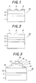
- the HBT 30 shown in Fig. 3 although the HBT 30 has an npn-type junction structure, it may have a pnp-type junction structure by changing the conduction types of the semiconductor layers of the HBT 30. Moreover, for developing the crystal qualities of the conductive layers 13-16 formed on the underlayer 2, a buffer layer or a multilayered structure such as a distorted superlattice structure may be provided between the underlayer 2 and the conductive layer 13.
Landscapes
- Junction Field-Effect Transistors (AREA)
- Chemical Vapour Deposition (AREA)
- Bipolar Transistors (AREA)
- Crystals, And After-Treatments Of Crystals (AREA)
Applications Claiming Priority (6)
| Application Number | Priority Date | Filing Date | Title |
|---|---|---|---|
| JP2000373039 | 2000-12-07 | ||
| JP2000373039 | 2000-12-07 | ||
| JP2001153693 | 2001-05-23 | ||
| JP2001153693 | 2001-05-23 | ||
| JP2001267299A JP3836697B2 (ja) | 2000-12-07 | 2001-09-04 | 半導体素子 |
| JP2001267299 | 2001-09-04 |
Publications (2)
| Publication Number | Publication Date |
|---|---|
| EP1213767A2 true EP1213767A2 (fr) | 2002-06-12 |
| EP1213767A3 EP1213767A3 (fr) | 2004-04-14 |
Family
ID=27345391
Family Applications (1)
| Application Number | Title | Priority Date | Filing Date |
|---|---|---|---|
| EP01128995A Withdrawn EP1213767A3 (fr) | 2000-12-07 | 2001-12-06 | Elément semi-conducteur en composé de nitrure |
Country Status (3)
| Country | Link |
|---|---|
| US (3) | US6583468B2 (fr) |
| EP (1) | EP1213767A3 (fr) |
| JP (1) | JP3836697B2 (fr) |
Cited By (4)
| Publication number | Priority date | Publication date | Assignee | Title |
|---|---|---|---|---|
| US6703649B2 (en) | 2001-05-31 | 2004-03-09 | Ngk Insulators, Ltd. | Semiconductor element |
| EP1431426A3 (fr) * | 2002-12-18 | 2006-10-04 | Ngk Insulators, Ltd. | Substrat pour croissance épitaxiale |
| US7183578B2 (en) | 2003-03-26 | 2007-02-27 | Kyocera Corporation | Semiconductor apparatus, method for growing nitride semiconductor and method for producing semiconductor apparatus |
| CN104246980A (zh) * | 2012-04-26 | 2014-12-24 | 应用材料公司 | 用于led制造的pvd缓冲层 |
Families Citing this family (36)
| Publication number | Priority date | Publication date | Assignee | Title |
|---|---|---|---|---|
| JP4327339B2 (ja) * | 2000-07-28 | 2009-09-09 | 独立行政法人物質・材料研究機構 | 半導体層形成用基板とそれを利用した半導体装置 |
| JP3886341B2 (ja) * | 2001-05-21 | 2007-02-28 | 日本電気株式会社 | 窒化ガリウム結晶基板の製造方法及び窒化ガリウム結晶基板 |
| JP3954335B2 (ja) * | 2001-06-15 | 2007-08-08 | 日本碍子株式会社 | Iii族窒化物多層膜 |
| JP4514727B2 (ja) * | 2001-12-25 | 2010-07-28 | 日本碍子株式会社 | Iii族窒化物膜の製造方法、iii族窒化物膜、iii族窒化物素子用エピタキシャル基板、及びiii族窒化物素子 |
| KR100484486B1 (ko) * | 2002-10-18 | 2005-04-20 | 한국전자통신연구원 | 질화물 반도체 전계 효과 트랜지스터 및 그 제조방법 |
| JP2004289005A (ja) * | 2003-03-24 | 2004-10-14 | Ngk Insulators Ltd | エピタキシャル基板、半導体素子および高電子移動度トランジスタ |
| JP2004327882A (ja) * | 2003-04-28 | 2004-11-18 | Ngk Insulators Ltd | エピタキシャル基板、半導体素子および高電子移動度トランジスタ |
| US7078743B2 (en) * | 2003-05-15 | 2006-07-18 | Matsushita Electric Industrial Co., Ltd. | Field effect transistor semiconductor device |
| JP2005136200A (ja) * | 2003-10-30 | 2005-05-26 | Univ Nagoya | 窒化物半導体結晶層の作製方法、窒化物半導体結晶層、及び窒化物半導体結晶層作製用の基材 |
| US7238970B2 (en) * | 2003-10-30 | 2007-07-03 | Matsushita Electric Industrial Co., Ltd. | Semiconductor device and method for fabricating the same |
| US6987300B2 (en) * | 2004-03-25 | 2006-01-17 | Microchip Technology Incorporated | High voltage ESD-protection structure |
| US7981744B2 (en) | 2004-06-10 | 2011-07-19 | Toyoda Gosei Co., Ltd. | Field-effect transistor, semiconductor device, a method for manufacturing them, and a method of semiconductor crystal growth |
| JP2006032911A (ja) * | 2004-06-15 | 2006-02-02 | Ngk Insulators Ltd | 半導体積層構造、半導体素子およびhemt素子 |
| JP4712450B2 (ja) * | 2004-06-29 | 2011-06-29 | 日本碍子株式会社 | AlN結晶の表面平坦性改善方法 |
| US7339255B2 (en) * | 2004-08-24 | 2008-03-04 | Kabushiki Kaisha Toshiba | Semiconductor device having bidirectionally inclined toward <1-100> and <11-20> relative to {0001} crystal planes |
| WO2006098242A1 (fr) | 2005-03-17 | 2006-09-21 | Nec Corporation | Dispositif electrique enrobe d’un film et son procede de fabrication |
| JP5135686B2 (ja) * | 2005-03-23 | 2013-02-06 | 住友電気工業株式会社 | Iii族窒化物半導体素子 |
| JP4432827B2 (ja) * | 2005-04-26 | 2010-03-17 | 住友電気工業株式会社 | Iii族窒化物半導体素子およびエピタキシャル基板 |
| JP4984425B2 (ja) * | 2005-04-28 | 2012-07-25 | 住友電気工業株式会社 | 電界効果トランジスタおよびエピタキシャル基板 |
| EP1978550A4 (fr) | 2005-12-28 | 2009-07-22 | Nec Corp | Transistor a effet de champ, et film epitaxial multicouche pour un usage dans la preparation de transistor a effet de champ |
| JP4670055B2 (ja) * | 2006-03-20 | 2011-04-13 | Dowaエレクトロニクス株式会社 | 半導体基板及び半導体装置 |
| US7494546B1 (en) * | 2006-07-14 | 2009-02-24 | Blue Wave Semicodnuctors, Inc. | Method of growing insulating, semiconducting, and conducting group III-nitride thin films and coatings, and use as radiation hard coatings for electronics and optoelectronic devices |
| JP5311765B2 (ja) * | 2006-09-15 | 2013-10-09 | 住友化学株式会社 | 半導体エピタキシャル結晶基板およびその製造方法 |
| JP4712683B2 (ja) * | 2006-12-21 | 2011-06-29 | パナソニック株式会社 | トランジスタおよびその製造方法 |
| JP2008205221A (ja) * | 2007-02-20 | 2008-09-04 | Furukawa Electric Co Ltd:The | 半導体素子 |
| US8304809B2 (en) * | 2007-11-16 | 2012-11-06 | Furukawa Electric Co., Ltd. | GaN-based semiconductor device and method of manufacturing the same |
| JP2010206020A (ja) * | 2009-03-04 | 2010-09-16 | Panasonic Corp | 半導体装置 |
| JP5193150B2 (ja) * | 2009-09-24 | 2013-05-08 | 日本電信電話株式会社 | 窒化物半導体素子およびその製造方法 |
| JP2012015304A (ja) * | 2010-06-30 | 2012-01-19 | Sumitomo Electric Ind Ltd | 半導体装置 |
| JP2012015303A (ja) * | 2010-06-30 | 2012-01-19 | Sumitomo Electric Ind Ltd | 半導体基板および半導体装置 |
| JP5455875B2 (ja) * | 2010-11-25 | 2014-03-26 | 日本碍子株式会社 | エピタキシャル基板の製造方法 |
| JP2015133354A (ja) * | 2014-01-09 | 2015-07-23 | 日立金属株式会社 | 窒化物半導体エピタキシャルウェハ及び窒化物半導体デバイス |
| US10636663B2 (en) | 2017-03-29 | 2020-04-28 | Toyoda Gosei Co., Ltd. | Method of manufacturing semiconductor device including implanting impurities into an implanted region of a semiconductor layer and annealing the implanted region |
| CN111164733B (zh) * | 2017-07-20 | 2024-03-19 | 斯维甘公司 | 用于高电子迁移率晶体管的异质结构及其生产方法 |
| WO2019059381A1 (fr) * | 2017-09-22 | 2019-03-28 | 株式会社トクヤマ | Substrat monocristallin de nitrure du groupe iii |
| US12094958B2 (en) * | 2019-12-05 | 2024-09-17 | Enkris Semiconductor, Inc. | Semiconductor structures and manufacturing methods thereof |
Citations (2)
| Publication number | Priority date | Publication date | Assignee | Title |
|---|---|---|---|---|
| WO1998035388A1 (fr) | 1995-11-09 | 1998-08-13 | Northrop Grumman Corporation | Transistor bipolaire a heterojonction, a base de nitrure d'aluminium-gallium |
| EP1211736A2 (fr) * | 2000-11-30 | 2002-06-05 | Ngk Insulators, Ltd. | Dispositif semi-conducteur émetteur de lumière |
Family Cites Families (9)
| Publication number | Priority date | Publication date | Assignee | Title |
|---|---|---|---|---|
| DE69431333T2 (de) * | 1993-10-08 | 2003-07-31 | Mitsubishi Cable Industries, Ltd. | GaN-Einkristall |
| US5679965A (en) * | 1995-03-29 | 1997-10-21 | North Carolina State University | Integrated heterostructures of Group III-V nitride semiconductor materials including epitaxial ohmic contact, non-nitride buffer layer and methods of fabricating same |
| JPH0964477A (ja) * | 1995-08-25 | 1997-03-07 | Toshiba Corp | 半導体発光素子及びその製造方法 |
| JPH10199896A (ja) * | 1997-01-07 | 1998-07-31 | Fujitsu Ltd | 半導体装置の製造方法および半導体装置 |
| JPH10335637A (ja) * | 1997-05-30 | 1998-12-18 | Sony Corp | ヘテロ接合電界効果トランジスタ |
| JPH11340147A (ja) | 1998-05-25 | 1999-12-10 | Matsushita Electron Corp | 窒化物半導体ウエハーの製造方法および窒化物半導体素子の製造方法 |
| TW418549B (en) * | 1998-06-26 | 2001-01-11 | Sharp Kk | Crystal growth method for nitride semiconductor, nitride semiconductor light emitting device, and method for producing the same |
| US6252261B1 (en) * | 1998-09-30 | 2001-06-26 | Nec Corporation | GaN crystal film, a group III element nitride semiconductor wafer and a manufacturing process therefor |
| CN1557024B (zh) * | 2001-07-24 | 2010-04-07 | 美商克立股份有限公司 | 绝缘栅铝镓氮化物/氮化钾高电子迁移率晶体管(hemt) |
-
2001
- 2001-09-04 JP JP2001267299A patent/JP3836697B2/ja not_active Expired - Lifetime
- 2001-12-04 US US10/007,099 patent/US6583468B2/en not_active Expired - Lifetime
- 2001-12-06 EP EP01128995A patent/EP1213767A3/fr not_active Withdrawn
-
2003
- 2003-02-18 US US10/370,350 patent/US6707076B2/en not_active Expired - Lifetime
- 2003-10-21 US US10/690,290 patent/US6781164B2/en not_active Expired - Lifetime
Patent Citations (2)
| Publication number | Priority date | Publication date | Assignee | Title |
|---|---|---|---|---|
| WO1998035388A1 (fr) | 1995-11-09 | 1998-08-13 | Northrop Grumman Corporation | Transistor bipolaire a heterojonction, a base de nitrure d'aluminium-gallium |
| EP1211736A2 (fr) * | 2000-11-30 | 2002-06-05 | Ngk Insulators, Ltd. | Dispositif semi-conducteur émetteur de lumière |
Cited By (5)
| Publication number | Priority date | Publication date | Assignee | Title |
|---|---|---|---|---|
| US6703649B2 (en) | 2001-05-31 | 2004-03-09 | Ngk Insulators, Ltd. | Semiconductor element |
| EP1431426A3 (fr) * | 2002-12-18 | 2006-10-04 | Ngk Insulators, Ltd. | Substrat pour croissance épitaxiale |
| US7183578B2 (en) | 2003-03-26 | 2007-02-27 | Kyocera Corporation | Semiconductor apparatus, method for growing nitride semiconductor and method for producing semiconductor apparatus |
| CN104246980A (zh) * | 2012-04-26 | 2014-12-24 | 应用材料公司 | 用于led制造的pvd缓冲层 |
| US11011676B2 (en) | 2012-04-26 | 2021-05-18 | Applied Materials, Inc. | PVD buffer layers for LED fabrication |
Also Published As
| Publication number | Publication date |
|---|---|
| US6583468B2 (en) | 2003-06-24 |
| US6781164B2 (en) | 2004-08-24 |
| US20020113249A1 (en) | 2002-08-22 |
| EP1213767A3 (fr) | 2004-04-14 |
| US20030151065A1 (en) | 2003-08-14 |
| JP2003045899A (ja) | 2003-02-14 |
| JP3836697B2 (ja) | 2006-10-25 |
| US20040079964A1 (en) | 2004-04-29 |
| US6707076B2 (en) | 2004-03-16 |
Similar Documents
| Publication | Publication Date | Title |
|---|---|---|
| US6583468B2 (en) | Semiconductor element | |
| EP1875515B1 (fr) | Transistors a mobilite d'electrons elevee a base de nitrure binaire de groupe iii, et procedes permettant de produire ceux-ci | |
| US7709859B2 (en) | Cap layers including aluminum nitride for nitride-based transistors | |
| US6534801B2 (en) | GaN-based high electron mobility transistor | |
| JP4990496B2 (ja) | 窒化物ベースのトランジスタ及びその製造方法 | |
| US7547928B2 (en) | AlGaN/GaN high electron mobility transistor devices | |
| KR101124937B1 (ko) | 질화물계 트랜지스터를 위한 캡층 및/또는 패시베이션층,트랜지스터 구조 및 그 제조방법 | |
| US20070018198A1 (en) | High electron mobility electronic device structures comprising native substrates and methods for making the same | |
| US20080113497A1 (en) | SEMICONDUCTOR DEVICE ON GaN SUBSTRATE HAVING SURFACE BIDIRECTIONALLY INCLINED TOWARD <1-100> AND <11-20> DIRECTIONS RELATIVE TO {0001} CRYSTAL PLANES | |
| US20060118819A1 (en) | III-nitride material structures including silicon substrates | |
| JP4458223B2 (ja) | 化合物半導体素子及びその製造方法 | |
| EP2273553B1 (fr) | Méthode de fabrication de dispositifs HEMT en AlGaN/GaN | |
| JP2003059948A (ja) | 半導体装置及びその製造方法 | |
| US6703649B2 (en) | Semiconductor element | |
| KR20150085724A (ko) | 질화물 반도체 소자 및 그 제조 방법 | |
| JP3753068B2 (ja) | 電界効果トランジスタ用エピタキシャルウェハの製造方法 | |
| JP2006114652A (ja) | 半導体エピタキシャルウェハ及び電界効果トランジスタ | |
| JP2006114655A (ja) | 半導体エピタキシャルウェハ及び電界効果トランジスタ | |
| CN113224154B (zh) | 高电子迁移率晶体管及其制作方法 | |
| JP2004289005A (ja) | エピタキシャル基板、半導体素子および高電子移動度トランジスタ | |
| JP2000196067A (ja) | 窒化物系iii―v族化合物半導体装置 | |
| JP3987360B2 (ja) | エピタキシャル基板、電子デバイス用エピタキシャル基板、及び電子デバイス | |
| KR20150000752A (ko) | 질화물 반도체 소자 및 그 제조 방법 | |
| JP2006114653A (ja) | 半導体エピタキシャルウェハ及び電界効果トランジスタ | |
| JP2006196557A (ja) | 半導体エピタキシャルウェハ及び電界効果トランジスタ |
Legal Events
| Date | Code | Title | Description |
|---|---|---|---|
| PUAI | Public reference made under article 153(3) epc to a published international application that has entered the european phase |
Free format text: ORIGINAL CODE: 0009012 |
|
| AK | Designated contracting states |
Kind code of ref document: A2 Designated state(s): AT BE CH CY DE DK ES FI FR GB GR IE IT LI LU MC NL PT SE TR |
|
| AX | Request for extension of the european patent |
Free format text: AL;LT;LV;MK;RO;SI |
|
| PUAL | Search report despatched |
Free format text: ORIGINAL CODE: 0009013 |
|
| RIC1 | Information provided on ipc code assigned before grant |
Ipc: 7H 01L 29/20 A |
|
| AK | Designated contracting states |
Kind code of ref document: A3 Designated state(s): AT BE CH CY DE DK ES FI FR GB GR IE IT LI LU MC NL PT SE TR |
|
| AX | Request for extension of the european patent |
Extension state: AL LT LV MK RO SI |
|
| 17P | Request for examination filed |
Effective date: 20040825 |
|
| AKX | Designation fees paid |
Designated state(s): AT BE CH CY DE DK ES FI FR GB GR IE IT LI LU MC NL PT SE TR |
|
| 17Q | First examination report despatched |
Effective date: 20081114 |
|
| GRAP | Despatch of communication of intention to grant a patent |
Free format text: ORIGINAL CODE: EPIDOSNIGR1 |
|
| RIC1 | Information provided on ipc code assigned before grant |
Ipc: H01L 29/20 20060101AFI20160929BHEP Ipc: H01L 21/02 20060101ALI20160929BHEP Ipc: H01L 29/66 20060101ALI20160929BHEP |
|
| INTG | Intention to grant announced |
Effective date: 20161019 |
|
| STAA | Information on the status of an ep patent application or granted ep patent |
Free format text: STATUS: THE APPLICATION IS DEEMED TO BE WITHDRAWN |
|
| 18D | Application deemed to be withdrawn |
Effective date: 20170301 |