JP4265437B2 - 光回路基板の製造方法及び光回路基板 - Google Patents
光回路基板の製造方法及び光回路基板 Download PDFInfo
- Publication number
- JP4265437B2 JP4265437B2 JP2004046360A JP2004046360A JP4265437B2 JP 4265437 B2 JP4265437 B2 JP 4265437B2 JP 2004046360 A JP2004046360 A JP 2004046360A JP 2004046360 A JP2004046360 A JP 2004046360A JP 4265437 B2 JP4265437 B2 JP 4265437B2
- Authority
- JP
- Japan
- Prior art keywords
- core
- resin layer
- optical
- circuit board
- light
- Prior art date
- Legal status (The legal status is an assumption and is not a legal conclusion. Google has not performed a legal analysis and makes no representation as to the accuracy of the status listed.)
- Expired - Fee Related
Links
Images



Landscapes
- Optical Integrated Circuits (AREA)
Description
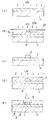
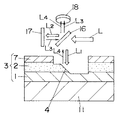
2 コア
3 光導波路
4 傾斜面
5 光偏向器
6 コア用樹脂層
7 被覆樹脂層
8 平面板
Claims (3)
- クラッドとコアとから形成される光導波路を備えると共に、コアの端面を傾斜面に形成して光を偏向入射させあるいは偏向出射させる光偏向器を設けた光回路基板を製造するにあたって、クラッドの上にコア用樹脂層を形成した後、コア用樹脂層に選択的に光を照射して導波路パターン形状のコアを形成すると共に現像してコア以外のコア用樹脂層を除去し、次にコアを覆うように樹脂を被覆して上面が平坦な被覆樹脂層を形成し、被覆樹脂層
の上からレーザを照射してコアの上に被覆される被覆樹脂層及びコアの上部を除去すると共に、コアの上部のこの除去は断面形状が円弧状の凸形状に形成される部分より深く行ない、この除去した部分に露出する箇所においてコアに光偏向器の傾斜面を形成する加工を行なうことを特徴とする光回路基板の製造方法。 - コアより屈折率が小さい樹脂の樹脂液をコアを覆うように塗布した後、この樹脂液の上に平面板を重ねた状態で樹脂液を硬化させることによって、上面が平坦な被覆樹脂層を形成することを特徴とする請求項1に記載の光回路基板の製造方法。
- 請求項1又は請求項2に記載の方法で製造されて成ることを特徴とする光回路基板。
Priority Applications (1)
| Application Number | Priority Date | Filing Date | Title |
|---|---|---|---|
| JP2004046360A JP4265437B2 (ja) | 2004-02-23 | 2004-02-23 | 光回路基板の製造方法及び光回路基板 |
Applications Claiming Priority (1)
| Application Number | Priority Date | Filing Date | Title |
|---|---|---|---|
| JP2004046360A JP4265437B2 (ja) | 2004-02-23 | 2004-02-23 | 光回路基板の製造方法及び光回路基板 |
Publications (2)
| Publication Number | Publication Date |
|---|---|
| JP2005234456A JP2005234456A (ja) | 2005-09-02 |
| JP4265437B2 true JP4265437B2 (ja) | 2009-05-20 |
Family
ID=35017443
Family Applications (1)
| Application Number | Title | Priority Date | Filing Date |
|---|---|---|---|
| JP2004046360A Expired - Fee Related JP4265437B2 (ja) | 2004-02-23 | 2004-02-23 | 光回路基板の製造方法及び光回路基板 |
Country Status (1)
| Country | Link |
|---|---|
| JP (1) | JP4265437B2 (ja) |
-
2004
- 2004-02-23 JP JP2004046360A patent/JP4265437B2/ja not_active Expired - Fee Related
Also Published As
| Publication number | Publication date |
|---|---|
| JP2005234456A (ja) | 2005-09-02 |
Similar Documents
| Publication | Publication Date | Title |
|---|---|---|
| JP5239835B2 (ja) | 光導波路及び光導波路型タッチパネル | |
| JP6123681B2 (ja) | ミラー付き光導波路及び光ファイバコネクタとその製造方法 | |
| TWI435127B (zh) | 光波導纖核之製造方法,光波導之製造方法,光波導以及光電複合線路板 | |
| JP2010169722A (ja) | 光学素子の製造方法及び光学素子 | |
| JP5319954B2 (ja) | 傾斜端面を有する光導波路の製造方法 | |
| JP2005195651A (ja) | 光接続基板、光伝送システム、及び製造方法 | |
| US8236374B2 (en) | Method of manufacturing optical waveguide device | |
| KR20110138178A (ko) | 광도파로 디바이스 | |
| CN106233176B (zh) | 光栅元件的安装结构的制造方法 | |
| JP2000298221A (ja) | 光導波路の製造方法および光送受信装置の製造方法 | |
| JP2009103827A (ja) | 光電複合基板及びその製造方法 | |
| JP4131222B2 (ja) | 光回路板の製造方法 | |
| JP3666463B2 (ja) | 光導波路デバイスおよび光導波路デバイスの製造方法 | |
| CN111033336A (zh) | 光波导、光电混载基板和它们的制造方法及光电混载模块 | |
| JP7185165B2 (ja) | 光導波路チップ | |
| JP2005234456A (ja) | 光回路基板の製造方法及び光回路基板 | |
| JP2009192842A (ja) | 光導波路及び成形型。 | |
| CN101726795A (zh) | 光波导装置制造方法 | |
| JP2007183467A (ja) | ミラー付光導波路及びその製造方法 | |
| JP2007183468A (ja) | ミラー付光導波路の製造方法 | |
| US7593610B2 (en) | Multi-mode optical coherence device and fabrication method thereof | |
| JP2003207661A (ja) | 光導波路装置 | |
| JPWO2004025343A1 (ja) | 光デバイス及びその製造方法 | |
| JP4277840B2 (ja) | 光導波路デバイスの製造方法 | |
| JP2004354537A (ja) | 微細構造体製造用マスターモデルの製造法と微細構造体製造用マスターモデル及び微細構造体 |
Legal Events
| Date | Code | Title | Description |
|---|---|---|---|
| A621 | Written request for application examination |
Free format text: JAPANESE INTERMEDIATE CODE: A621 Effective date: 20061213 |
|
| A977 | Report on retrieval |
Free format text: JAPANESE INTERMEDIATE CODE: A971007 Effective date: 20081021 |
|
| A131 | Notification of reasons for refusal |
Free format text: JAPANESE INTERMEDIATE CODE: A131 Effective date: 20081028 |
|
| A521 | Written amendment |
Free format text: JAPANESE INTERMEDIATE CODE: A523 Effective date: 20090105 |
|
| TRDD | Decision of grant or rejection written | ||
| A01 | Written decision to grant a patent or to grant a registration (utility model) |
Free format text: JAPANESE INTERMEDIATE CODE: A01 Effective date: 20090127 |
|
| A01 | Written decision to grant a patent or to grant a registration (utility model) |
Free format text: JAPANESE INTERMEDIATE CODE: A01 |
|
| A61 | First payment of annual fees (during grant procedure) |
Free format text: JAPANESE INTERMEDIATE CODE: A61 Effective date: 20090209 |
|
| R151 | Written notification of patent or utility model registration |
Ref document number: 4265437 Country of ref document: JP Free format text: JAPANESE INTERMEDIATE CODE: R151 |
|
| FPAY | Renewal fee payment (event date is renewal date of database) |
Free format text: PAYMENT UNTIL: 20120227 Year of fee payment: 3 |
|
| FPAY | Renewal fee payment (event date is renewal date of database) |
Free format text: PAYMENT UNTIL: 20130227 Year of fee payment: 4 |
|
| FPAY | Renewal fee payment (event date is renewal date of database) |
Free format text: PAYMENT UNTIL: 20130227 Year of fee payment: 4 |
|
| FPAY | Renewal fee payment (event date is renewal date of database) |
Free format text: PAYMENT UNTIL: 20140227 Year of fee payment: 5 |
|
| LAPS | Cancellation because of no payment of annual fees |