JP4507582B2 - バンプ付電子部品の実装方法 - Google Patents
バンプ付電子部品の実装方法 Download PDFInfo
- Publication number
- JP4507582B2 JP4507582B2 JP2003414476A JP2003414476A JP4507582B2 JP 4507582 B2 JP4507582 B2 JP 4507582B2 JP 2003414476 A JP2003414476 A JP 2003414476A JP 2003414476 A JP2003414476 A JP 2003414476A JP 4507582 B2 JP4507582 B2 JP 4507582B2
- Authority
- JP
- Japan
- Prior art keywords
- electronic component
- metal
- electrode
- bump
- substrate
- Prior art date
- Legal status (The legal status is an assumption and is not a legal conclusion. Google has not performed a legal analysis and makes no representation as to the accuracy of the status listed.)
- Expired - Lifetime
Links
Images

Classifications
-
- H—ELECTRICITY
- H10—SEMICONDUCTOR DEVICES; ELECTRIC SOLID-STATE DEVICES NOT OTHERWISE PROVIDED FOR
- H10W—GENERIC PACKAGES, INTERCONNECTIONS, CONNECTORS OR OTHER CONSTRUCTIONAL DETAILS OF DEVICES COVERED BY CLASS H10
- H10W72/00—Interconnections or connectors in packages
- H10W72/071—Connecting or disconnecting
-
- B—PERFORMING OPERATIONS; TRANSPORTING
- B23—MACHINE TOOLS; METAL-WORKING NOT OTHERWISE PROVIDED FOR
- B23K—SOLDERING OR UNSOLDERING; WELDING; CLADDING OR PLATING BY SOLDERING OR WELDING; CUTTING BY APPLYING HEAT LOCALLY, e.g. FLAME CUTTING; WORKING BY LASER BEAM
- B23K20/00—Non-electric welding by applying impact or other pressure, with or without the application of heat, e.g. cladding or plating
- B23K20/10—Non-electric welding by applying impact or other pressure, with or without the application of heat, e.g. cladding or plating making use of vibrations, e.g. ultrasonic welding
-
- H—ELECTRICITY
- H10—SEMICONDUCTOR DEVICES; ELECTRIC SOLID-STATE DEVICES NOT OTHERWISE PROVIDED FOR
- H10W—GENERIC PACKAGES, INTERCONNECTIONS, CONNECTORS OR OTHER CONSTRUCTIONAL DETAILS OF DEVICES COVERED BY CLASS H10
- H10W72/00—Interconnections or connectors in packages
- H10W72/071—Connecting or disconnecting
- H10W72/0711—Apparatus therefor
- H10W72/07178—Means for aligning
-
- H—ELECTRICITY
- H10—SEMICONDUCTOR DEVICES; ELECTRIC SOLID-STATE DEVICES NOT OTHERWISE PROVIDED FOR
- H10W—GENERIC PACKAGES, INTERCONNECTIONS, CONNECTORS OR OTHER CONSTRUCTIONAL DETAILS OF DEVICES COVERED BY CLASS H10
- H10W72/00—Interconnections or connectors in packages
- H10W72/071—Connecting or disconnecting
- H10W72/072—Connecting or disconnecting of bump connectors
- H10W72/07231—Techniques
- H10W72/07236—Soldering or alloying
-
- H—ELECTRICITY
- H10—SEMICONDUCTOR DEVICES; ELECTRIC SOLID-STATE DEVICES NOT OTHERWISE PROVIDED FOR
- H10W—GENERIC PACKAGES, INTERCONNECTIONS, CONNECTORS OR OTHER CONSTRUCTIONAL DETAILS OF DEVICES COVERED BY CLASS H10
- H10W72/00—Interconnections or connectors in packages
- H10W72/071—Connecting or disconnecting
- H10W72/072—Connecting or disconnecting of bump connectors
- H10W72/07251—Connecting or disconnecting of bump connectors characterised by changes in properties of the bump connectors during connecting
-
- H—ELECTRICITY
- H10—SEMICONDUCTOR DEVICES; ELECTRIC SOLID-STATE DEVICES NOT OTHERWISE PROVIDED FOR
- H10W—GENERIC PACKAGES, INTERCONNECTIONS, CONNECTORS OR OTHER CONSTRUCTIONAL DETAILS OF DEVICES COVERED BY CLASS H10
- H10W72/00—Interconnections or connectors in packages
- H10W72/071—Connecting or disconnecting
- H10W72/073—Connecting or disconnecting of die-attach connectors
-
- H—ELECTRICITY
- H10—SEMICONDUCTOR DEVICES; ELECTRIC SOLID-STATE DEVICES NOT OTHERWISE PROVIDED FOR
- H10W—GENERIC PACKAGES, INTERCONNECTIONS, CONNECTORS OR OTHER CONSTRUCTIONAL DETAILS OF DEVICES COVERED BY CLASS H10
- H10W72/00—Interconnections or connectors in packages
- H10W72/20—Bump connectors, e.g. solder bumps or copper pillars; Dummy bumps; Thermal bumps
-
- H—ELECTRICITY
- H10—SEMICONDUCTOR DEVICES; ELECTRIC SOLID-STATE DEVICES NOT OTHERWISE PROVIDED FOR
- H10W—GENERIC PACKAGES, INTERCONNECTIONS, CONNECTORS OR OTHER CONSTRUCTIONAL DETAILS OF DEVICES COVERED BY CLASS H10
- H10W72/00—Interconnections or connectors in packages
- H10W72/20—Bump connectors, e.g. solder bumps or copper pillars; Dummy bumps; Thermal bumps
- H10W72/251—Materials
- H10W72/252—Materials comprising solid metals or solid metalloids, e.g. PbSn, Ag or Cu
-
- H—ELECTRICITY
- H10—SEMICONDUCTOR DEVICES; ELECTRIC SOLID-STATE DEVICES NOT OTHERWISE PROVIDED FOR
- H10W—GENERIC PACKAGES, INTERCONNECTIONS, CONNECTORS OR OTHER CONSTRUCTIONAL DETAILS OF DEVICES COVERED BY CLASS H10
- H10W72/00—Interconnections or connectors in packages
- H10W72/90—Bond pads, in general
-
- H—ELECTRICITY
- H10—SEMICONDUCTOR DEVICES; ELECTRIC SOLID-STATE DEVICES NOT OTHERWISE PROVIDED FOR
- H10W—GENERIC PACKAGES, INTERCONNECTIONS, CONNECTORS OR OTHER CONSTRUCTIONAL DETAILS OF DEVICES COVERED BY CLASS H10
- H10W72/00—Interconnections or connectors in packages
- H10W72/90—Bond pads, in general
- H10W72/941—Dispositions of bond pads
- H10W72/9415—Dispositions of bond pads relative to the surface, e.g. recessed, protruding
-
- H—ELECTRICITY
- H10—SEMICONDUCTOR DEVICES; ELECTRIC SOLID-STATE DEVICES NOT OTHERWISE PROVIDED FOR
- H10W—GENERIC PACKAGES, INTERCONNECTIONS, CONNECTORS OR OTHER CONSTRUCTIONAL DETAILS OF DEVICES COVERED BY CLASS H10
- H10W72/00—Interconnections or connectors in packages
- H10W72/90—Bond pads, in general
- H10W72/951—Materials of bond pads
- H10W72/952—Materials of bond pads comprising metals or metalloids, e.g. PbSn, Ag or Cu
Landscapes
- Engineering & Computer Science (AREA)
- Mechanical Engineering (AREA)
- Wire Bonding (AREA)
- Electric Connection Of Electric Components To Printed Circuits (AREA)
Description
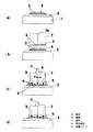
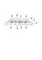
、そのうちの一部の金属バンプ6を電極3に金属接合した段階で、超音波振動を実質的に停止する工程とを含む形態となっている。
3 電極
4 樹脂
5 電子部品
6 金属バンプ
Claims (4)
- 複数の金属バンプが形成されたバンプ付電子部品を複数の電極が形成された基板に実装するバンプ付電子部品の実装方法であって、前記バンプ付電子部品と前記基板との間に熱硬化性の樹脂を介在させた状態で前記複数の金属バンプを前記複数の電極に位置合わせする工程と、前記バンプ付電子部品に超音波振動と熱と加圧力を作用させながらこのバンプ付電子部品を基板に対して押圧する工程と、全ての金属バンプを前記電極に接触させて電気的に接続するとともにそのうちの一部の金属バンプを前記電極に金属接合した段階で前記超音波振動を実質的に停止する工程と、前記超音波振動を実質的に停止した後も、前記バンプ付電子部品に対して熱と加圧力を継続して作用させることにより前記熱硬化性樹脂の硬化を進展させる工程を含むことを特徴とするバンプ付電子部品の実装方法。
- 前記バンプ付電子部品の背面にツールを接触させ、このツールを介してバンプ付電子部品に超音波振動と熱と加圧力を作用させることを特徴とする請求項1記載のバンプ付電子部品の実装方法。
- 前記金属バンプが金バンプであることを特徴とする請求項1記載のバンプ付電子部品の実装方法。
- 前記基板の電極上に予め前記樹脂を供給した後、前記金属バンプを前記樹脂で覆われた電極に位置合わせすることを特徴とする請求項1記載のバンプ付電子部品の実装方法。
Priority Applications (5)
| Application Number | Priority Date | Filing Date | Title |
|---|---|---|---|
| JP2003414476A JP4507582B2 (ja) | 2003-12-12 | 2003-12-12 | バンプ付電子部品の実装方法 |
| US11/009,451 US7284686B2 (en) | 2003-12-12 | 2004-12-10 | Mounting method of bump-equipped electronic component and mounting structure of the same |
| TW093138345A TW200527565A (en) | 2003-12-12 | 2004-12-10 | Mounting method of bump-equipped electronic component and mounting structure of the same |
| KR1020040104962A KR101093060B1 (ko) | 2003-12-12 | 2004-12-13 | 범프 부착 전자 부품의 실장 방법 및 구조 |
| CNB200410100227XA CN100382265C (zh) | 2003-12-12 | 2004-12-13 | 配备凸块的电子元件的安装方法及其安装结构 |
Applications Claiming Priority (1)
| Application Number | Priority Date | Filing Date | Title |
|---|---|---|---|
| JP2003414476A JP4507582B2 (ja) | 2003-12-12 | 2003-12-12 | バンプ付電子部品の実装方法 |
Publications (2)
| Publication Number | Publication Date |
|---|---|
| JP2005175250A JP2005175250A (ja) | 2005-06-30 |
| JP4507582B2 true JP4507582B2 (ja) | 2010-07-21 |
Family
ID=34650534
Family Applications (1)
| Application Number | Title | Priority Date | Filing Date |
|---|---|---|---|
| JP2003414476A Expired - Lifetime JP4507582B2 (ja) | 2003-12-12 | 2003-12-12 | バンプ付電子部品の実装方法 |
Country Status (5)
| Country | Link |
|---|---|
| US (1) | US7284686B2 (ja) |
| JP (1) | JP4507582B2 (ja) |
| KR (1) | KR101093060B1 (ja) |
| CN (1) | CN100382265C (ja) |
| TW (1) | TW200527565A (ja) |
Families Citing this family (6)
| Publication number | Priority date | Publication date | Assignee | Title |
|---|---|---|---|---|
| US7708654B2 (en) * | 2002-05-29 | 2010-05-04 | Acushnet Company | Foam-core golf balls |
| US8715110B2 (en) | 2003-05-19 | 2014-05-06 | Acushnet Company | Foam-core golf balls |
| JP4863746B2 (ja) * | 2006-03-27 | 2012-01-25 | 富士通株式会社 | 半導体装置およびその製造方法 |
| CN101728289B (zh) * | 2008-10-10 | 2011-12-28 | 哈尔滨工业大学深圳研究生院 | 一种面阵封装电子元件的室温超声波软钎焊方法 |
| US20130256885A1 (en) * | 2012-04-03 | 2013-10-03 | Conexant Systems, Inc. | Copper Sphere Array Package |
| CN104409370B (zh) * | 2014-11-18 | 2017-06-13 | 通富微电子股份有限公司 | 一种钉头凸点芯片的倒装装片方法及施加装片压力的方法 |
Family Cites Families (12)
| Publication number | Priority date | Publication date | Assignee | Title |
|---|---|---|---|---|
| US5192015A (en) * | 1991-11-20 | 1993-03-09 | Santa Barbara Research Center | Method for wire bonding |
| JP3308855B2 (ja) * | 1997-05-27 | 2002-07-29 | 三菱電機株式会社 | 半導体装置の製造方法 |
| JP3176580B2 (ja) * | 1998-04-09 | 2001-06-18 | 太陽誘電株式会社 | 電子部品の実装方法及び実装装置 |
| EP1156520A4 (en) * | 1999-01-29 | 2004-08-25 | Matsushita Electric Industrial Co Ltd | ASSEMBLY METHOD FOR ELECTRONIC COMPONENTS AND THEIR DEVICE |
| JP2001244298A (ja) * | 2000-02-28 | 2001-09-07 | Toshiba Corp | フリップチップ接続方法 |
| JP2001298146A (ja) * | 2000-04-13 | 2001-10-26 | Mitsubishi Electric Corp | 多層配線基体の製造方法および多層配線基体 |
| JP3491827B2 (ja) * | 2000-07-25 | 2004-01-26 | 関西日本電気株式会社 | 半導体装置及びその製造方法 |
| JP2002151551A (ja) * | 2000-11-10 | 2002-05-24 | Hitachi Ltd | フリップチップ実装構造、その実装構造を有する半導体装置及び実装方法 |
| BR0105083A (pt) * | 2000-11-17 | 2002-06-25 | Goodyear Tire & Rubber | Composição de borracha leve contendo argila |
| JP3891838B2 (ja) * | 2001-12-26 | 2007-03-14 | 株式会社ルネサステクノロジ | 半導体装置およびその製造方法 |
| JP3721559B2 (ja) * | 2002-03-28 | 2005-11-30 | 東レエンジニアリング株式会社 | チップ実装方法 |
| US20070075436A1 (en) * | 2003-10-06 | 2007-04-05 | Nec Corporation | Electronic device and manufacturing method of the same |
-
2003
- 2003-12-12 JP JP2003414476A patent/JP4507582B2/ja not_active Expired - Lifetime
-
2004
- 2004-12-10 US US11/009,451 patent/US7284686B2/en not_active Expired - Lifetime
- 2004-12-10 TW TW093138345A patent/TW200527565A/zh unknown
- 2004-12-13 KR KR1020040104962A patent/KR101093060B1/ko not_active Expired - Fee Related
- 2004-12-13 CN CNB200410100227XA patent/CN100382265C/zh not_active Expired - Lifetime
Also Published As
| Publication number | Publication date |
|---|---|
| US20050127141A1 (en) | 2005-06-16 |
| TW200527565A (en) | 2005-08-16 |
| JP2005175250A (ja) | 2005-06-30 |
| KR101093060B1 (ko) | 2011-12-13 |
| CN100382265C (zh) | 2008-04-16 |
| KR20050058985A (ko) | 2005-06-17 |
| CN1627493A (zh) | 2005-06-15 |
| US7284686B2 (en) | 2007-10-23 |
Similar Documents
| Publication | Publication Date | Title |
|---|---|---|
| JP4507582B2 (ja) | バンプ付電子部品の実装方法 | |
| JP2005150311A (ja) | チップマウント方法及び装置 | |
| JP3376861B2 (ja) | バンプ付きワークの実装方法 | |
| CN100409430C (zh) | 半导体器件和半导体器件的组装方法 | |
| JPH09115954A (ja) | フリップチップ実装方法 | |
| JP3726795B2 (ja) | バンプ付きワークの実装方法 | |
| JPH07122591A (ja) | 半導体装置の実装方法 | |
| JP2002141373A (ja) | 半導体実装方法および半導体実装装置 | |
| JPH1174315A (ja) | ボンディング装置及びボンディング方法 | |
| JP2009004462A (ja) | 半導体装置の実装方法 | |
| JP4378227B2 (ja) | フリップチップ実装方法 | |
| JP3915317B2 (ja) | 電子部品の実装方法 | |
| JPH11288975A (ja) | ボンディング方法及びボンディング装置 | |
| JPH11288975A5 (ja) | ||
| JP3960076B2 (ja) | 電子部品実装方法 | |
| JPH11135561A (ja) | 異方性導電接着フィルム、その製造方法、フリップチップ実装方法、およびフリップチップ実装基板 | |
| JP2002289644A (ja) | 半導体素子の接合方法及び接合装置 | |
| JP4295517B2 (ja) | 半導体チップの実装構造および半導体チップの実装方法 | |
| JP3646677B2 (ja) | 表示パネル | |
| JP2002270637A (ja) | フリップチップ接続方法およびチップボンディング装置 | |
| JP2004235472A (ja) | 半導体装置の製造方法 | |
| JP2000323526A (ja) | 電子部品の実装方法 | |
| JPH1050771A (ja) | バンプ付電子部品の実装方法及び回路モジュール | |
| JP5858600B2 (ja) | チップ実装方法 | |
| JP2008300638A (ja) | ベアチップのフリップチップ実装方法 |
Legal Events
| Date | Code | Title | Description |
|---|---|---|---|
| A621 | Written request for application examination |
Free format text: JAPANESE INTERMEDIATE CODE: A621 Effective date: 20061212 |
|
| RD01 | Notification of change of attorney |
Free format text: JAPANESE INTERMEDIATE CODE: A7421 Effective date: 20070112 |
|
| A977 | Report on retrieval |
Free format text: JAPANESE INTERMEDIATE CODE: A971007 Effective date: 20081209 |
|
| A131 | Notification of reasons for refusal |
Free format text: JAPANESE INTERMEDIATE CODE: A131 Effective date: 20090804 |
|
| A521 | Request for written amendment filed |
Free format text: JAPANESE INTERMEDIATE CODE: A523 Effective date: 20090928 |
|
| RD01 | Notification of change of attorney |
Free format text: JAPANESE INTERMEDIATE CODE: A7421 Effective date: 20091120 |
|
| A131 | Notification of reasons for refusal |
Free format text: JAPANESE INTERMEDIATE CODE: A131 Effective date: 20091215 |
|
| TRDD | Decision of grant or rejection written | ||
| A01 | Written decision to grant a patent or to grant a registration (utility model) |
Free format text: JAPANESE INTERMEDIATE CODE: A01 Effective date: 20100413 |
|
| A01 | Written decision to grant a patent or to grant a registration (utility model) |
Free format text: JAPANESE INTERMEDIATE CODE: A01 |
|
| A61 | First payment of annual fees (during grant procedure) |
Free format text: JAPANESE INTERMEDIATE CODE: A61 Effective date: 20100426 |
|
| FPAY | Renewal fee payment (event date is renewal date of database) |
Free format text: PAYMENT UNTIL: 20130514 Year of fee payment: 3 |
|
| R151 | Written notification of patent or utility model registration |
Ref document number: 4507582 Country of ref document: JP Free format text: JAPANESE INTERMEDIATE CODE: R151 |
|
| FPAY | Renewal fee payment (event date is renewal date of database) |
Free format text: PAYMENT UNTIL: 20130514 Year of fee payment: 3 |
|
| FPAY | Renewal fee payment (event date is renewal date of database) |
Free format text: PAYMENT UNTIL: 20130514 Year of fee payment: 3 |
|
| EXPY | Cancellation because of completion of term |