JP4597183B2 - 半導体装置の製造方法 - Google Patents
半導体装置の製造方法 Download PDFInfo
- Publication number
- JP4597183B2 JP4597183B2 JP2007312675A JP2007312675A JP4597183B2 JP 4597183 B2 JP4597183 B2 JP 4597183B2 JP 2007312675 A JP2007312675 A JP 2007312675A JP 2007312675 A JP2007312675 A JP 2007312675A JP 4597183 B2 JP4597183 B2 JP 4597183B2
- Authority
- JP
- Japan
- Prior art keywords
- semiconductor chip
- semiconductor
- internal electrode
- hole
- metal
- Prior art date
- Legal status (The legal status is an assumption and is not a legal conclusion. Google has not performed a legal analysis and makes no representation as to the accuracy of the status listed.)
- Expired - Lifetime
Links
Images





Classifications
-
- H—ELECTRICITY
- H10—SEMICONDUCTOR DEVICES; ELECTRIC SOLID-STATE DEVICES NOT OTHERWISE PROVIDED FOR
- H10W—GENERIC PACKAGES, INTERCONNECTIONS, CONNECTORS OR OTHER CONSTRUCTIONAL DETAILS OF DEVICES COVERED BY CLASS H10
- H10W72/00—Interconnections or connectors in packages
- H10W72/50—Bond wires
- H10W72/531—Shapes of wire connectors
- H10W72/536—Shapes of wire connectors the connected ends being ball-shaped
-
- H—ELECTRICITY
- H10—SEMICONDUCTOR DEVICES; ELECTRIC SOLID-STATE DEVICES NOT OTHERWISE PROVIDED FOR
- H10W—GENERIC PACKAGES, INTERCONNECTIONS, CONNECTORS OR OTHER CONSTRUCTIONAL DETAILS OF DEVICES COVERED BY CLASS H10
- H10W72/00—Interconnections or connectors in packages
- H10W72/50—Bond wires
- H10W72/531—Shapes of wire connectors
- H10W72/5363—Shapes of wire connectors the connected ends being wedge-shaped
-
- H—ELECTRICITY
- H10—SEMICONDUCTOR DEVICES; ELECTRIC SOLID-STATE DEVICES NOT OTHERWISE PROVIDED FOR
- H10W—GENERIC PACKAGES, INTERCONNECTIONS, CONNECTORS OR OTHER CONSTRUCTIONAL DETAILS OF DEVICES COVERED BY CLASS H10
- H10W90/00—Package configurations
- H10W90/701—Package configurations characterised by the relative positions of pads or connectors relative to package parts
- H10W90/721—Package configurations characterised by the relative positions of pads or connectors relative to package parts of bump connectors
- H10W90/722—Package configurations characterised by the relative positions of pads or connectors relative to package parts of bump connectors between stacked chips
-
- H—ELECTRICITY
- H10—SEMICONDUCTOR DEVICES; ELECTRIC SOLID-STATE DEVICES NOT OTHERWISE PROVIDED FOR
- H10W—GENERIC PACKAGES, INTERCONNECTIONS, CONNECTORS OR OTHER CONSTRUCTIONAL DETAILS OF DEVICES COVERED BY CLASS H10
- H10W90/00—Package configurations
- H10W90/701—Package configurations characterised by the relative positions of pads or connectors relative to package parts
- H10W90/751—Package configurations characterised by the relative positions of pads or connectors relative to package parts of bond wires
- H10W90/756—Package configurations characterised by the relative positions of pads or connectors relative to package parts of bond wires between a chip and a stacked lead frame, conducting package substrate or heat sink
Landscapes
- Internal Circuitry In Semiconductor Integrated Circuit Devices (AREA)
- Electrodes Of Semiconductors (AREA)
Description
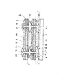
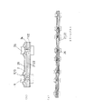
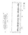
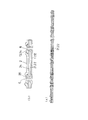
2 半導体チップの保護膜
3 第1の半導体チップの外部電極
4 第1の半導体チップの内部電極
5 接着剤
6 貫通孔
7 第2の半導体チップ
8 第2の半導体チップの内部電極
9 第3のチップ
10 第3のチップの内部電極
11 第2の半導体チップの酸化膜
12 第3の半導体チップの酸化膜
13 第2のめっき電極
14 第3のめっき電極
15 めっき電極
16 ダイボンド樹脂
17 リードフレームのリード
18 リードフレームのダイパッド
19 ボンディングワイヤ
20 封止樹脂
21 第2の半導体チップよりなるウエハ
22 第3の半導体チップよりなるウエハ
23 無電解めっき液
24 無電解めっき槽
25 めっき金属膜
26 レジスト
27 エッチング液
28 エッチング槽
29 第1の半導体チップのウエハ
30 コレット
31 コレットの真空孔
32 ダイシングの溝
33 絶縁樹脂
34 酸化膜
Claims (4)
- 第1の半導体チップに積層される第2の半導体チップの内部電極に前記第2の半導体チップを貫通する貫通孔を設ける工程と、
前記貫通孔内壁および裏面に絶縁膜を形成する工程と、
前記貫通孔内壁に第1の金属を無電解めっきまたは蒸着により形成する工程と、
前記第1および第2の半導体チップの内部電極同士が対応するように、前記第1の半導体チップに対して間隙を有した状態で前記第2の半導体チップを前記第1の半導体チップの外部電極および内部電極を除く部分に接着固定する工程と、
前記第2の半導体チップの内部電極および貫通孔内壁の前記第1の金属と前記第1の半導体チップの内部電極を無電解めっきにより電気的に接続する工程とを含む半導体装置の製造方法。 - 第1の半導体チップに積層される第2の半導体チップの内部電極に前記第2の半導体チップを貫通する貫通孔を設ける工程と、
前記貫通孔内壁および裏面に絶縁膜を形成する工程と、
前記貫通孔内壁に第1の金属を無電解めっきまたは蒸着により形成する工程と、
前記第1および第2の半導体チップの内部電極同士が対応するように、前記第1の半導体チップに対して間隙を有した状態で前記第2の半導体チップを前記第1の半導体チップの外部電極および内部電極を除く部分に接着固定する工程と、
前記第2の半導体チップ上にさらに1個以上の第2の半導体チップを下層および上層の第2の半導体チップの内部電極同士が対応するように配置し、前記下層の第2の半導体チップに対して前記上層の第2の半導体チップが間隙を有した状態で前記上層の第2の半導体チップを前記下層の第2の半導体チップの内部電極を除く部分に接着固定する工程と、
前記第2の半導体チップの内部電極および貫通孔内壁の前記第1の金属と前記第1の半導体チップの内部電極を無電解めっきにより電気的に接続する工程とを含む半導体装置の製造方法。 - 前記貫通孔内壁に記第1の金属としてCu,Ni,Au,Pt,Ag,Sn等を形成する工程を有することを特徴とする請求項1または2記載の半導体装置の製造方法。
- 前記第2の半導体チップの内部電極および貫通孔内壁の前記第1の金属と前記第1の半導体チップの内部電極を無電解めっきにより電気的に接続する工程において、無電解めっきによりNiあるいはAuをめっきすることを特徴とする請求項1または2記載の半導体装置の製造方法。
Priority Applications (1)
| Application Number | Priority Date | Filing Date | Title |
|---|---|---|---|
| JP2007312675A JP4597183B2 (ja) | 2007-12-03 | 2007-12-03 | 半導体装置の製造方法 |
Applications Claiming Priority (1)
| Application Number | Priority Date | Filing Date | Title |
|---|---|---|---|
| JP2007312675A JP4597183B2 (ja) | 2007-12-03 | 2007-12-03 | 半導体装置の製造方法 |
Related Parent Applications (1)
| Application Number | Title | Priority Date | Filing Date |
|---|---|---|---|
| JP31222299A Division JP4245754B2 (ja) | 1999-11-02 | 1999-11-02 | 半導体装置 |
Publications (2)
| Publication Number | Publication Date |
|---|---|
| JP2008072150A JP2008072150A (ja) | 2008-03-27 |
| JP4597183B2 true JP4597183B2 (ja) | 2010-12-15 |
Family
ID=39293404
Family Applications (1)
| Application Number | Title | Priority Date | Filing Date |
|---|---|---|---|
| JP2007312675A Expired - Lifetime JP4597183B2 (ja) | 2007-12-03 | 2007-12-03 | 半導体装置の製造方法 |
Country Status (1)
| Country | Link |
|---|---|
| JP (1) | JP4597183B2 (ja) |
Family Cites Families (4)
| Publication number | Priority date | Publication date | Assignee | Title |
|---|---|---|---|---|
| JPH0563137A (ja) * | 1991-08-30 | 1993-03-12 | Fujitsu Ltd | 半導体装置 |
| JPH06268151A (ja) * | 1993-03-12 | 1994-09-22 | Rohm Co Ltd | 半導体装置 |
| JP3186941B2 (ja) * | 1995-02-07 | 2001-07-11 | シャープ株式会社 | 半導体チップおよびマルチチップ半導体モジュール |
| JPH09270490A (ja) * | 1995-10-31 | 1997-10-14 | Nkk Corp | 接続部構造および接続方法並びに半導体装置およびその製造方法 |
-
2007
- 2007-12-03 JP JP2007312675A patent/JP4597183B2/ja not_active Expired - Lifetime
Also Published As
| Publication number | Publication date |
|---|---|
| JP2008072150A (ja) | 2008-03-27 |
Similar Documents
| Publication | Publication Date | Title |
|---|---|---|
| CN109216296B (zh) | 半导体封装件和方法 | |
| CN107919345B (zh) | 芯片的叠层封装结构及叠层封装方法 | |
| JP4245754B2 (ja) | 半導体装置 | |
| US10177130B2 (en) | Semiconductor assembly having anti-warping controller and vertical connecting element in stiffener | |
| TW202543095A (zh) | 形成具有增進可濕側翼的經封裝半導體裝置的方法及結構 | |
| TWI749088B (zh) | 半導體裝置的製造方法 | |
| US7923835B2 (en) | Package, electronic device, substrate having a separation region and a wiring layers, and method for manufacturing | |
| JPWO2012137714A1 (ja) | 半導体装置および半導体装置の製造方法 | |
| US8361857B2 (en) | Semiconductor device having a simplified stack and method for manufacturing thereof | |
| US20250343199A1 (en) | Electronic device and manufacturing method thereof | |
| US7420814B2 (en) | Package stack and manufacturing method thereof | |
| JP2005294443A (ja) | 半導体装置及びその製造方法 | |
| US9112063B2 (en) | Fabrication method of semiconductor package | |
| JP2004363573A (ja) | 半導体チップ実装体およびその製造方法 | |
| TWI512925B (zh) | 焊線結構及形成焊線結構的方法 | |
| JP3468132B2 (ja) | 半導体装置の製造方法 | |
| JP4597183B2 (ja) | 半導体装置の製造方法 | |
| JP2023060343A (ja) | 半導体モジュール | |
| KR20080045017A (ko) | 금속 범프를 갖는 반도체 칩 패키지 및 그 제조방법 | |
| CN116207080A (zh) | 半导体器件和用于使用激光开槽减少金属毛刺的方法 | |
| KR101128999B1 (ko) | 칩 패키지 제조 방법 및 이에 의해 제조된 칩 패키지 | |
| CN100446244C (zh) | 半导体芯片安装体及其制造方法 | |
| KR100608331B1 (ko) | 멀티 칩 패키지 | |
| JP3674550B2 (ja) | 半導体装置 | |
| JP2003298007A (ja) | 半導体装置およびその製造方法 |
Legal Events
| Date | Code | Title | Description |
|---|---|---|---|
| TRDD | Decision of grant or rejection written | ||
| A01 | Written decision to grant a patent or to grant a registration (utility model) |
Free format text: JAPANESE INTERMEDIATE CODE: A01 Effective date: 20100831 |
|
| A01 | Written decision to grant a patent or to grant a registration (utility model) |
Free format text: JAPANESE INTERMEDIATE CODE: A01 |
|
| A61 | First payment of annual fees (during grant procedure) |
Free format text: JAPANESE INTERMEDIATE CODE: A61 Effective date: 20100921 |
|
| R151 | Written notification of patent or utility model registration |
Ref document number: 4597183 Country of ref document: JP Free format text: JAPANESE INTERMEDIATE CODE: R151 |
|
| FPAY | Renewal fee payment (event date is renewal date of database) |
Free format text: PAYMENT UNTIL: 20131001 Year of fee payment: 3 |
|
| S111 | Request for change of ownership or part of ownership |
Free format text: JAPANESE INTERMEDIATE CODE: R313113 |
|
| R350 | Written notification of registration of transfer |
Free format text: JAPANESE INTERMEDIATE CODE: R350 |
|
| R250 | Receipt of annual fees |
Free format text: JAPANESE INTERMEDIATE CODE: R250 |
|
| R250 | Receipt of annual fees |
Free format text: JAPANESE INTERMEDIATE CODE: R250 |
|
| R250 | Receipt of annual fees |
Free format text: JAPANESE INTERMEDIATE CODE: R250 |
|
| R250 | Receipt of annual fees |
Free format text: JAPANESE INTERMEDIATE CODE: R250 |
|
| R250 | Receipt of annual fees |
Free format text: JAPANESE INTERMEDIATE CODE: R250 |
|
| EXPY | Cancellation because of completion of term |