JP4641817B2 - 半導体装置用積層基板の製造方法及び半導体装置 - Google Patents
半導体装置用積層基板の製造方法及び半導体装置 Download PDFInfo
- Publication number
- JP4641817B2 JP4641817B2 JP2005033672A JP2005033672A JP4641817B2 JP 4641817 B2 JP4641817 B2 JP 4641817B2 JP 2005033672 A JP2005033672 A JP 2005033672A JP 2005033672 A JP2005033672 A JP 2005033672A JP 4641817 B2 JP4641817 B2 JP 4641817B2
- Authority
- JP
- Japan
- Prior art keywords
- layer
- silicon
- substrate
- semiconductor device
- diamond
- Prior art date
- Legal status (The legal status is an assumption and is not a legal conclusion. Google has not performed a legal analysis and makes no representation as to the accuracy of the status listed.)
- Expired - Fee Related
Links
Images



Classifications
-
- H—ELECTRICITY
- H10—SEMICONDUCTOR DEVICES; ELECTRIC SOLID-STATE DEVICES NOT OTHERWISE PROVIDED FOR
- H10P—GENERIC PROCESSES OR APPARATUS FOR THE MANUFACTURE OR TREATMENT OF DEVICES COVERED BY CLASS H10
- H10P14/00—Formation of materials, e.g. in the shape of layers or pillars
- H10P14/60—Formation of materials, e.g. in the shape of layers or pillars of insulating materials
- H10P14/66—Formation of materials, e.g. in the shape of layers or pillars of insulating materials characterised by the type of materials
- H10P14/662—Laminate layers, e.g. stacks of alternating high-k metal oxides
-
- C—CHEMISTRY; METALLURGY
- C23—COATING METALLIC MATERIAL; COATING MATERIAL WITH METALLIC MATERIAL; CHEMICAL SURFACE TREATMENT; DIFFUSION TREATMENT OF METALLIC MATERIAL; COATING BY VACUUM EVAPORATION, BY SPUTTERING, BY ION IMPLANTATION OR BY CHEMICAL VAPOUR DEPOSITION, IN GENERAL; INHIBITING CORROSION OF METALLIC MATERIAL OR INCRUSTATION IN GENERAL
- C23C—COATING METALLIC MATERIAL; COATING MATERIAL WITH METALLIC MATERIAL; SURFACE TREATMENT OF METALLIC MATERIAL BY DIFFUSION INTO THE SURFACE, BY CHEMICAL CONVERSION OR SUBSTITUTION; COATING BY VACUUM EVAPORATION, BY SPUTTERING, BY ION IMPLANTATION OR BY CHEMICAL VAPOUR DEPOSITION, IN GENERAL
- C23C16/00—Chemical coating by decomposition of gaseous compounds, without leaving reaction products of surface material in the coating, i.e. chemical vapour deposition [CVD] processes
- C23C16/01—Chemical coating by decomposition of gaseous compounds, without leaving reaction products of surface material in the coating, i.e. chemical vapour deposition [CVD] processes on temporary substrates, e.g. substrates subsequently removed by etching
-
- A—HUMAN NECESSITIES
- A61—MEDICAL OR VETERINARY SCIENCE; HYGIENE
- A61C—DENTISTRY; APPARATUS OR METHODS FOR ORAL OR DENTAL HYGIENE
- A61C8/00—Means to be fixed to the jaw-bone for consolidating natural teeth or for fixing dental prostheses thereon; Dental implants; Implanting tools
- A61C8/0089—Implanting tools or instruments
-
- A—HUMAN NECESSITIES
- A61—MEDICAL OR VETERINARY SCIENCE; HYGIENE
- A61B—DIAGNOSIS; SURGERY; IDENTIFICATION
- A61B17/00—Surgical instruments, devices or methods
- A61B17/16—Instruments for performing osteoclasis; Drills or chisels for bones; Trepans
- A61B17/1662—Instruments for performing osteoclasis; Drills or chisels for bones; Trepans for particular parts of the body
- A61B17/1673—Instruments for performing osteoclasis; Drills or chisels for bones; Trepans for particular parts of the body for the jaw
-
- A—HUMAN NECESSITIES
- A61—MEDICAL OR VETERINARY SCIENCE; HYGIENE
- A61C—DENTISTRY; APPARATUS OR METHODS FOR ORAL OR DENTAL HYGIENE
- A61C1/00—Dental machines for boring or cutting ; General features of dental machines or apparatus, e.g. hand-piece design
- A61C1/08—Machine parts specially adapted for dentistry
- A61C1/082—Positioning or guiding, e.g. of drills
- A61C1/084—Positioning or guiding, e.g. of drills of implanting tools
-
- A—HUMAN NECESSITIES
- A61—MEDICAL OR VETERINARY SCIENCE; HYGIENE
- A61C—DENTISTRY; APPARATUS OR METHODS FOR ORAL OR DENTAL HYGIENE
- A61C3/00—Dental tools or instruments
- A61C3/02—Tooth drilling or cutting instruments; Instruments acting like a sandblast machine
-
- A—HUMAN NECESSITIES
- A61—MEDICAL OR VETERINARY SCIENCE; HYGIENE
- A61C—DENTISTRY; APPARATUS OR METHODS FOR ORAL OR DENTAL HYGIENE
- A61C8/00—Means to be fixed to the jaw-bone for consolidating natural teeth or for fixing dental prostheses thereon; Dental implants; Implanting tools
- A61C8/0089—Implanting tools or instruments
- A61C8/009—Implanting tools or instruments for selecting the right implanting element, e.g. templates
-
- C—CHEMISTRY; METALLURGY
- C23—COATING METALLIC MATERIAL; COATING MATERIAL WITH METALLIC MATERIAL; CHEMICAL SURFACE TREATMENT; DIFFUSION TREATMENT OF METALLIC MATERIAL; COATING BY VACUUM EVAPORATION, BY SPUTTERING, BY ION IMPLANTATION OR BY CHEMICAL VAPOUR DEPOSITION, IN GENERAL; INHIBITING CORROSION OF METALLIC MATERIAL OR INCRUSTATION IN GENERAL
- C23C—COATING METALLIC MATERIAL; COATING MATERIAL WITH METALLIC MATERIAL; SURFACE TREATMENT OF METALLIC MATERIAL BY DIFFUSION INTO THE SURFACE, BY CHEMICAL CONVERSION OR SUBSTITUTION; COATING BY VACUUM EVAPORATION, BY SPUTTERING, BY ION IMPLANTATION OR BY CHEMICAL VAPOUR DEPOSITION, IN GENERAL
- C23C16/00—Chemical coating by decomposition of gaseous compounds, without leaving reaction products of surface material in the coating, i.e. chemical vapour deposition [CVD] processes
- C23C16/22—Chemical coating by decomposition of gaseous compounds, without leaving reaction products of surface material in the coating, i.e. chemical vapour deposition [CVD] processes characterised by the deposition of inorganic material, other than metallic material
- C23C16/26—Deposition of carbon only
- C23C16/27—Diamond only
- C23C16/274—Diamond only using microwave discharges
-
- C—CHEMISTRY; METALLURGY
- C23—COATING METALLIC MATERIAL; COATING MATERIAL WITH METALLIC MATERIAL; CHEMICAL SURFACE TREATMENT; DIFFUSION TREATMENT OF METALLIC MATERIAL; COATING BY VACUUM EVAPORATION, BY SPUTTERING, BY ION IMPLANTATION OR BY CHEMICAL VAPOUR DEPOSITION, IN GENERAL; INHIBITING CORROSION OF METALLIC MATERIAL OR INCRUSTATION IN GENERAL
- C23C—COATING METALLIC MATERIAL; COATING MATERIAL WITH METALLIC MATERIAL; SURFACE TREATMENT OF METALLIC MATERIAL BY DIFFUSION INTO THE SURFACE, BY CHEMICAL CONVERSION OR SUBSTITUTION; COATING BY VACUUM EVAPORATION, BY SPUTTERING, BY ION IMPLANTATION OR BY CHEMICAL VAPOUR DEPOSITION, IN GENERAL
- C23C16/00—Chemical coating by decomposition of gaseous compounds, without leaving reaction products of surface material in the coating, i.e. chemical vapour deposition [CVD] processes
- C23C16/22—Chemical coating by decomposition of gaseous compounds, without leaving reaction products of surface material in the coating, i.e. chemical vapour deposition [CVD] processes characterised by the deposition of inorganic material, other than metallic material
- C23C16/26—Deposition of carbon only
- C23C16/27—Diamond only
- C23C16/278—Diamond only doping or introduction of a secondary phase in the diamond
-
- C—CHEMISTRY; METALLURGY
- C23—COATING METALLIC MATERIAL; COATING MATERIAL WITH METALLIC MATERIAL; CHEMICAL SURFACE TREATMENT; DIFFUSION TREATMENT OF METALLIC MATERIAL; COATING BY VACUUM EVAPORATION, BY SPUTTERING, BY ION IMPLANTATION OR BY CHEMICAL VAPOUR DEPOSITION, IN GENERAL; INHIBITING CORROSION OF METALLIC MATERIAL OR INCRUSTATION IN GENERAL
- C23C—COATING METALLIC MATERIAL; COATING MATERIAL WITH METALLIC MATERIAL; SURFACE TREATMENT OF METALLIC MATERIAL BY DIFFUSION INTO THE SURFACE, BY CHEMICAL CONVERSION OR SUBSTITUTION; COATING BY VACUUM EVAPORATION, BY SPUTTERING, BY ION IMPLANTATION OR BY CHEMICAL VAPOUR DEPOSITION, IN GENERAL
- C23C16/00—Chemical coating by decomposition of gaseous compounds, without leaving reaction products of surface material in the coating, i.e. chemical vapour deposition [CVD] processes
- C23C16/56—After-treatment
-
- H—ELECTRICITY
- H10—SEMICONDUCTOR DEVICES; ELECTRIC SOLID-STATE DEVICES NOT OTHERWISE PROVIDED FOR
- H10D—INORGANIC ELECTRIC SEMICONDUCTOR DEVICES
- H10D62/00—Semiconductor bodies, or regions thereof, of devices having potential barriers
- H10D62/80—Semiconductor bodies, or regions thereof, of devices having potential barriers characterised by the materials
- H10D62/83—Semiconductor bodies, or regions thereof, of devices having potential barriers characterised by the materials being Group IV materials, e.g. B-doped Si or undoped Ge
- H10D62/8303—Diamond
-
- H—ELECTRICITY
- H10—SEMICONDUCTOR DEVICES; ELECTRIC SOLID-STATE DEVICES NOT OTHERWISE PROVIDED FOR
- H10P—GENERIC PROCESSES OR APPARATUS FOR THE MANUFACTURE OR TREATMENT OF DEVICES COVERED BY CLASS H10
- H10P14/00—Formation of materials, e.g. in the shape of layers or pillars
- H10P14/60—Formation of materials, e.g. in the shape of layers or pillars of insulating materials
- H10P14/69—Inorganic materials
- H10P14/6902—Inorganic materials composed of carbon, e.g. alpha-C, diamond or hydrogen doped carbon
-
- H—ELECTRICITY
- H10—SEMICONDUCTOR DEVICES; ELECTRIC SOLID-STATE DEVICES NOT OTHERWISE PROVIDED FOR
- H10P—GENERIC PROCESSES OR APPARATUS FOR THE MANUFACTURE OR TREATMENT OF DEVICES COVERED BY CLASS H10
- H10P14/00—Formation of materials, e.g. in the shape of layers or pillars
- H10P14/60—Formation of materials, e.g. in the shape of layers or pillars of insulating materials
- H10P14/69—Inorganic materials
- H10P14/6903—Inorganic materials containing silicon
-
- H—ELECTRICITY
- H10—SEMICONDUCTOR DEVICES; ELECTRIC SOLID-STATE DEVICES NOT OTHERWISE PROVIDED FOR
- H10P—GENERIC PROCESSES OR APPARATUS FOR THE MANUFACTURE OR TREATMENT OF DEVICES COVERED BY CLASS H10
- H10P90/00—Preparation of wafers not covered by a single main group of this subclass, e.g. wafer reinforcement
- H10P90/19—Preparing inhomogeneous wafers
- H10P90/1904—Preparing vertically inhomogeneous wafers
- H10P90/1906—Preparing SOI wafers
- H10P90/1922—Preparing SOI wafers using silicon etch back techniques, e.g. BESOI or ELTRAN
-
- H—ELECTRICITY
- H10—SEMICONDUCTOR DEVICES; ELECTRIC SOLID-STATE DEVICES NOT OTHERWISE PROVIDED FOR
- H10W—GENERIC PACKAGES, INTERCONNECTIONS, CONNECTORS OR OTHER CONSTRUCTIONAL DETAILS OF DEVICES COVERED BY CLASS H10
- H10W10/00—Isolation regions in semiconductor bodies between components of integrated devices
- H10W10/10—Isolation regions comprising dielectric materials
- H10W10/181—Semiconductor-on-insulator [SOI] isolation regions, e.g. buried oxide regions of SOI wafers
-
- H—ELECTRICITY
- H10—SEMICONDUCTOR DEVICES; ELECTRIC SOLID-STATE DEVICES NOT OTHERWISE PROVIDED FOR
- H10P—GENERIC PROCESSES OR APPARATUS FOR THE MANUFACTURE OR TREATMENT OF DEVICES COVERED BY CLASS H10
- H10P72/00—Handling or holding of wafers, substrates or devices during manufacture or treatment thereof
- H10P72/70—Handling or holding of wafers, substrates or devices during manufacture or treatment thereof for supporting or gripping
- H10P72/74—Handling or holding of wafers, substrates or devices during manufacture or treatment thereof for supporting or gripping using temporarily an auxiliary support
- H10P72/7432—Handling or holding of wafers, substrates or devices during manufacture or treatment thereof for supporting or gripping using temporarily an auxiliary support used in a transfer process involving transfer directly from an origin substrate to a target substrate without use of an intermediate handle substrate
Landscapes
- Chemical & Material Sciences (AREA)
- Health & Medical Sciences (AREA)
- Engineering & Computer Science (AREA)
- General Chemical & Material Sciences (AREA)
- Organic Chemistry (AREA)
- Metallurgy (AREA)
- Mechanical Engineering (AREA)
- Materials Engineering (AREA)
- Chemical Kinetics & Catalysis (AREA)
- Oral & Maxillofacial Surgery (AREA)
- Life Sciences & Earth Sciences (AREA)
- General Health & Medical Sciences (AREA)
- Veterinary Medicine (AREA)
- Public Health (AREA)
- Animal Behavior & Ethology (AREA)
- Dentistry (AREA)
- Inorganic Chemistry (AREA)
- Epidemiology (AREA)
- Orthopedic Medicine & Surgery (AREA)
- Surgery (AREA)
- Nuclear Medicine, Radiotherapy & Molecular Imaging (AREA)
- Biomedical Technology (AREA)
- Heart & Thoracic Surgery (AREA)
- Medical Informatics (AREA)
- Molecular Biology (AREA)
- Recrystallisation Techniques (AREA)
- Chemical Vapour Deposition (AREA)
- Crystals, And After-Treatments Of Crystals (AREA)
- Element Separation (AREA)
Description
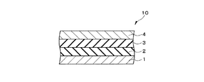
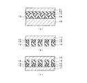
2、12;SiO2層
3、14、113;ダイヤモンド層
4、15、112;シリコン層
6;ポリシリコン膜
7;SiO2膜
10、20、100;積層基板
13;アモルファスシリコン層
17;アルミニウムマスク
114;多結晶シリコン層
Claims (12)
- 第1のシリコン基板の一方の面上にダイヤモンド層を形成する工程と、前記ダイヤモンド層上及び第2のシリコン基板上にシリコンを含有する層を形成する工程と、前記ダイヤモンド層と第2のシリコン基板とをシリコンを含有する層を介して接合する工程と、前記第1のシリコン基板を除去して前記ダイヤモンド層の表面を露出させる工程と、前記ダイヤモンド層上に半導体層を形成する工程と、を有することを特徴とする半導体装置用積層基板の製造方法。
- 前記ダイヤモンド層を局所的に形成することを特徴とする請求項1に記載の半導体装置用積層基板の製造方法。
- 前記第2のシリコン基板の前記一方の面における前記ダイヤモンド層が設けられていない領域上にも前記半導体層を形成することを特徴とする請求項2に記載の半導体装置用積層基板の製造方法。
- 前記ダイヤモンド層と前記第2のシリコン基板とを酸化シリコン層を介して接合することを特徴とする請求項1乃至3のいずれか1項に記載の半導体装置用積層基板の製造方法。
- 前記酸化シリコン層を、前記ダイヤモンド層及び前記第2のシリコン基板の双方の接合面上に形成しておくことを特徴とする請求項4に記載の半導体装置用積層基板の製造方法。
- 前記ダイヤモンド層と前記第2のシリコン基板とをアモルファスシリコン層を介して接合することを特徴とする請求項1乃至3のいずれか1項に記載の半導体装置用積層基板の製造方法。
- 前記アモルファスシリコン層を、前記ダイヤモンド層及び前記第2のシリコン基板の双方の接合面上に形成しておくことを特徴とする請求項6に記載の半導体装置用積層基板の製造方法。
- 前記ダイヤモンド層及び前記第2のシリコン基板のうち、一方の接合面に酸化シリコン層を形成すると共に他方の接合面にアモルファスシリコン層を形成しておき、前記酸化シリコン層及び前記アモルファスシリコン層を介して前記ダイヤモンド層と前記第2のシリコン基板とを接合することを特徴とする請求項1乃至3のいずれか1項に記載の半導体装置用積層基板の製造方法。
- 前記ダイヤモンド層と前記第2のシリコン基板とを熱圧着により接合することを特徴とする請求項4乃至8のいずれか1項に記載の半導体装置用積層基板の製造方法。
- 前記ダイヤモンド層は、ドーパンドがドープされた導電性ダイヤモンドにより形成されていることを特徴とする請求項1乃至9のいずれか1項に記載の半導体装置用積層基板の製造方法。
- 前記半導体層は、シリコン層であり、この半導体層に素子が形成されることを特徴とする請求項1乃至10のいずれか1項に記載の半導体装置用積層基板の製造方法。
- 請求項1乃至11のいずれか1項に記載の方法で製造された積層基板を有することを特徴とする半導体装置。
Priority Applications (4)
| Application Number | Priority Date | Filing Date | Title |
|---|---|---|---|
| JP2005033672A JP4641817B2 (ja) | 2005-02-09 | 2005-02-09 | 半導体装置用積層基板の製造方法及び半導体装置 |
| TW094147623A TWI308606B (en) | 2005-02-09 | 2005-12-30 | Semiconductor device and method for manufacturing multilayered substrate for semiconductor device |
| US11/328,162 US7285479B2 (en) | 2005-02-09 | 2006-01-10 | Semiconductor device and method for manufacturing multilayered substrate for semiconductor device |
| KR1020060012101A KR100740032B1 (ko) | 2005-02-09 | 2006-02-08 | 반도체 장치용 적층 기판의 제조 방법 및 반도체 장치 |
Applications Claiming Priority (1)
| Application Number | Priority Date | Filing Date | Title |
|---|---|---|---|
| JP2005033672A JP4641817B2 (ja) | 2005-02-09 | 2005-02-09 | 半導体装置用積層基板の製造方法及び半導体装置 |
Publications (2)
| Publication Number | Publication Date |
|---|---|
| JP2006222236A JP2006222236A (ja) | 2006-08-24 |
| JP4641817B2 true JP4641817B2 (ja) | 2011-03-02 |
Family
ID=36778891
Family Applications (1)
| Application Number | Title | Priority Date | Filing Date |
|---|---|---|---|
| JP2005033672A Expired - Fee Related JP4641817B2 (ja) | 2005-02-09 | 2005-02-09 | 半導体装置用積層基板の製造方法及び半導体装置 |
Country Status (4)
| Country | Link |
|---|---|
| US (1) | US7285479B2 (ja) |
| JP (1) | JP4641817B2 (ja) |
| KR (1) | KR100740032B1 (ja) |
| TW (1) | TWI308606B (ja) |
Families Citing this family (12)
| Publication number | Priority date | Publication date | Assignee | Title |
|---|---|---|---|---|
| US7344760B1 (en) * | 2003-09-12 | 2008-03-18 | The United States Of America As Represented By The Secretary Of The Navy | Wear-resistant electrically conductive body |
| TWI262853B (en) * | 2005-04-27 | 2006-10-01 | Kinik Co | Diamond substrate and method for fabricating the same |
| GB0721760D0 (en) * | 2007-11-06 | 2007-12-19 | Element Six Ltd | Composite material |
| FR2934713B1 (fr) * | 2008-07-29 | 2010-10-15 | Commissariat Energie Atomique | Substrat de type semi-conducteur sur isolant a couches de diamant intrinseque et dope |
| FR2938373A1 (fr) * | 2008-11-12 | 2010-05-14 | Commissariat Energie Atomique | Integration d'une couche de diamant polycristallin, notamment dans une structure sod |
| KR101080200B1 (ko) * | 2009-04-14 | 2011-11-07 | 주식회사 하이닉스반도체 | 반도체 메모리 장치 및 그 리프레쉬 제어 방법 |
| US10584412B2 (en) | 2016-03-08 | 2020-03-10 | Ii-Vi Delaware, Inc. | Substrate comprising a layer of silicon and a layer of diamond having an optically finished (or a dense) silicon-diamond interface |
| CN107665829B (zh) | 2017-08-24 | 2019-12-17 | 长江存储科技有限责任公司 | 晶圆混合键合中提高金属引线制程安全性的方法 |
| US12176221B2 (en) * | 2019-05-31 | 2024-12-24 | Texas State University | Incorporating semiconductors on a polycrystalline diamond substrate |
| WO2020263845A1 (en) * | 2019-06-24 | 2020-12-30 | Akash Systems, Inc. | Material growth on wide-bandgap semiconductor materials |
| US20240175123A1 (en) * | 2022-11-29 | 2024-05-30 | Phononics Ltd | Fusion bonding of diamond using thermal SiO2 |
| CN118957751A (zh) * | 2023-05-15 | 2024-11-15 | 香港大学 | 一种规模化制造超平多晶金刚石膜的方法 |
Family Cites Families (12)
| Publication number | Priority date | Publication date | Assignee | Title |
|---|---|---|---|---|
| US4169337A (en) * | 1978-03-30 | 1979-10-02 | Nalco Chemical Company | Process for polishing semi-conductor materials |
| US5131963A (en) * | 1987-11-16 | 1992-07-21 | Crystallume | Silicon on insulator semiconductor composition containing thin synthetic diamone films |
| JPH02206118A (ja) * | 1989-02-06 | 1990-08-15 | Hitachi Ltd | 半導体素子 |
| US5313094A (en) * | 1992-01-28 | 1994-05-17 | International Business Machines Corportion | Thermal dissipation of integrated circuits using diamond paths |
| US5276338A (en) * | 1992-05-15 | 1994-01-04 | International Business Machines Corporation | Bonded wafer structure having a buried insulation layer |
| US5552345A (en) * | 1993-09-22 | 1996-09-03 | Harris Corporation | Die separation method for silicon on diamond circuit structures |
| KR100335449B1 (ko) * | 1998-04-17 | 2002-05-04 | 가네꼬 히사시 | Soi 기판 및 그 제조 방법 |
| FR2781082B1 (fr) * | 1998-07-10 | 2002-09-20 | Commissariat Energie Atomique | Structure semiconductrice en couche mince comportant une couche de repartition de chaleur |
| JP3062163B2 (ja) | 1998-12-01 | 2000-07-10 | キヤノン販売株式会社 | 半導体装置及び半導体装置の膜の形成方法 |
| US6770966B2 (en) * | 2001-07-31 | 2004-08-03 | Intel Corporation | Electronic assembly including a die having an integrated circuit and a layer of diamond to transfer heat |
| JP2003261399A (ja) * | 2002-03-11 | 2003-09-16 | Shin Etsu Chem Co Ltd | ダイヤモンド製膜用基材およびダイヤモンド膜 |
| JP2004204299A (ja) * | 2002-12-25 | 2004-07-22 | Ebara Corp | ダイヤモンド成膜シリコンおよび電極 |
-
2005
- 2005-02-09 JP JP2005033672A patent/JP4641817B2/ja not_active Expired - Fee Related
- 2005-12-30 TW TW094147623A patent/TWI308606B/zh not_active IP Right Cessation
-
2006
- 2006-01-10 US US11/328,162 patent/US7285479B2/en not_active Expired - Fee Related
- 2006-02-08 KR KR1020060012101A patent/KR100740032B1/ko not_active Expired - Fee Related
Also Published As
| Publication number | Publication date |
|---|---|
| US20060175293A1 (en) | 2006-08-10 |
| US7285479B2 (en) | 2007-10-23 |
| TWI308606B (en) | 2009-04-11 |
| KR20060090613A (ko) | 2006-08-14 |
| TW200710292A (en) | 2007-03-16 |
| KR100740032B1 (ko) | 2007-07-18 |
| JP2006222236A (ja) | 2006-08-24 |
Similar Documents
| Publication | Publication Date | Title |
|---|---|---|
| JP2020161833A (ja) | 多結晶セラミック基板 | |
| JP5730393B2 (ja) | 複合基板およびその製造方法 | |
| JPH09500493A (ja) | ダイヤモンド絶縁体を組み込んだボンデッドウエハプロセス | |
| JP2006222236A (ja) | 半導体装置用積層基板の製造方法及び半導体装置 | |
| CN117012754A (zh) | 半导体结构及其形成方法 | |
| JPH0846031A (ja) | 貼り合わせシリコン基板の製造方法 | |
| JP5484578B2 (ja) | 複合基板および製造方法 | |
| TWI723378B (zh) | 絕緣體上覆矽基板的製造方法及半導體裝置 | |
| CN110491827A (zh) | 一种半导体薄膜层的转移方法及复合晶圆的制备方法 | |
| JP7006544B2 (ja) | Soiウェーハ及びその製造方法 | |
| JP3488927B2 (ja) | 誘電体分離基板及びその製造方法 | |
| JP2542609B2 (ja) | 半導体装置の製造方法 | |
| JPH08236615A (ja) | 誘電体分離基板及びその製造方法 | |
| JP4951580B2 (ja) | 半導体ウエハの製造方法 | |
| JP2013135175A (ja) | 複合基板およびその製造方法 | |
| JP2004320050A (ja) | Soi基板及びその製造方法 | |
| JP2608443B2 (ja) | 半導体ウエハの製造方法 | |
| TWI329923B (en) | Method of mandfacturing a semiconductor substrate | |
| JPH03292723A (ja) | シリコン単結晶薄膜の作製方法 | |
| WO2025215945A1 (ja) | 複合基板およびその製造方法 | |
| JP2007180365A (ja) | 半導体装置及びその製造方法 | |
| JPH05152180A (ja) | 半導体装置及び製造方法 | |
| JP2007250676A (ja) | 異種材料の積層基板の製造方法 | |
| CN115513123A (zh) | 一种绝缘体上硅结构及其形成方法 | |
| JPH0964168A (ja) | 複合半導体基板 |
Legal Events
| Date | Code | Title | Description |
|---|---|---|---|
| A621 | Written request for application examination |
Free format text: JAPANESE INTERMEDIATE CODE: A621 Effective date: 20070928 |
|
| A977 | Report on retrieval |
Free format text: JAPANESE INTERMEDIATE CODE: A971007 Effective date: 20080520 |
|
| A131 | Notification of reasons for refusal |
Free format text: JAPANESE INTERMEDIATE CODE: A131 Effective date: 20101005 |
|
| A521 | Request for written amendment filed |
Free format text: JAPANESE INTERMEDIATE CODE: A523 Effective date: 20101109 |
|
| TRDD | Decision of grant or rejection written | ||
| A01 | Written decision to grant a patent or to grant a registration (utility model) |
Free format text: JAPANESE INTERMEDIATE CODE: A01 Effective date: 20101130 |
|
| A01 | Written decision to grant a patent or to grant a registration (utility model) |
Free format text: JAPANESE INTERMEDIATE CODE: A01 |
|
| A61 | First payment of annual fees (during grant procedure) |
Free format text: JAPANESE INTERMEDIATE CODE: A61 Effective date: 20101130 |
|
| R150 | Certificate of patent or registration of utility model |
Free format text: JAPANESE INTERMEDIATE CODE: R150 |
|
| FPAY | Renewal fee payment (event date is renewal date of database) |
Free format text: PAYMENT UNTIL: 20131210 Year of fee payment: 3 |
|
| LAPS | Cancellation because of no payment of annual fees |