JP4816545B2 - 基板処理装置、基板処理方法及び記憶媒体 - Google Patents
基板処理装置、基板処理方法及び記憶媒体 Download PDFInfo
- Publication number
- JP4816545B2 JP4816545B2 JP2007095376A JP2007095376A JP4816545B2 JP 4816545 B2 JP4816545 B2 JP 4816545B2 JP 2007095376 A JP2007095376 A JP 2007095376A JP 2007095376 A JP2007095376 A JP 2007095376A JP 4816545 B2 JP4816545 B2 JP 4816545B2
- Authority
- JP
- Japan
- Prior art keywords
- substrate
- storage
- transfer
- storage shelf
- chamber
- Prior art date
- Legal status (The legal status is an assumption and is not a legal conclusion. Google has not performed a legal analysis and makes no representation as to the accuracy of the status listed.)
- Expired - Fee Related
Links
Images






Classifications
-
- H—ELECTRICITY
- H10—SEMICONDUCTOR DEVICES; ELECTRIC SOLID-STATE DEVICES NOT OTHERWISE PROVIDED FOR
- H10P—GENERIC PROCESSES OR APPARATUS FOR THE MANUFACTURE OR TREATMENT OF DEVICES COVERED BY CLASS H10
- H10P72/00—Handling or holding of wafers, substrates or devices during manufacture or treatment thereof
- H10P72/04—Apparatus for manufacture or treatment
- H10P72/0451—Apparatus for manufacturing or treating in a plurality of work-stations
- H10P72/0464—Apparatus for manufacturing or treating in a plurality of work-stations characterised by the construction of the transfer chamber
-
- H—ELECTRICITY
- H10—SEMICONDUCTOR DEVICES; ELECTRIC SOLID-STATE DEVICES NOT OTHERWISE PROVIDED FOR
- H10P—GENERIC PROCESSES OR APPARATUS FOR THE MANUFACTURE OR TREATMENT OF DEVICES COVERED BY CLASS H10
- H10P72/00—Handling or holding of wafers, substrates or devices during manufacture or treatment thereof
- H10P72/30—Handling or holding of wafers, substrates or devices during manufacture or treatment thereof for conveying, e.g. between different workstations
- H10P72/34—Handling or holding of wafers, substrates or devices during manufacture or treatment thereof for conveying, e.g. between different workstations the wafers being stored in a carrier, involving loading and unloading
- H10P72/3411—Handling or holding of wafers, substrates or devices during manufacture or treatment thereof for conveying, e.g. between different workstations the wafers being stored in a carrier, involving loading and unloading involving loading and unloading of wafers
-
- H—ELECTRICITY
- H10—SEMICONDUCTOR DEVICES; ELECTRIC SOLID-STATE DEVICES NOT OTHERWISE PROVIDED FOR
- H10P—GENERIC PROCESSES OR APPARATUS FOR THE MANUFACTURE OR TREATMENT OF DEVICES COVERED BY CLASS H10
- H10P72/00—Handling or holding of wafers, substrates or devices during manufacture or treatment thereof
- H10P72/04—Apparatus for manufacture or treatment
- H10P72/0451—Apparatus for manufacturing or treating in a plurality of work-stations
- H10P72/0466—Apparatus for manufacturing or treating in a plurality of work-stations characterised by the construction of the load-lock chamber
-
- H—ELECTRICITY
- H10—SEMICONDUCTOR DEVICES; ELECTRIC SOLID-STATE DEVICES NOT OTHERWISE PROVIDED FOR
- H10P—GENERIC PROCESSES OR APPARATUS FOR THE MANUFACTURE OR TREATMENT OF DEVICES COVERED BY CLASS H10
- H10P72/00—Handling or holding of wafers, substrates or devices during manufacture or treatment thereof
- H10P72/10—Handling or holding of wafers, substrates or devices during manufacture or treatment thereof using carriers specially adapted therefor, e.g. front opening unified pods [FOUP]
- H10P72/19—Handling or holding of wafers, substrates or devices during manufacture or treatment thereof using carriers specially adapted therefor, e.g. front opening unified pods [FOUP] closed carriers
- H10P72/1924—Handling or holding of wafers, substrates or devices during manufacture or treatment thereof using carriers specially adapted therefor, e.g. front opening unified pods [FOUP] closed carriers characterised by atmosphere control
-
- H—ELECTRICITY
- H10—SEMICONDUCTOR DEVICES; ELECTRIC SOLID-STATE DEVICES NOT OTHERWISE PROVIDED FOR
- H10P—GENERIC PROCESSES OR APPARATUS FOR THE MANUFACTURE OR TREATMENT OF DEVICES COVERED BY CLASS H10
- H10P72/00—Handling or holding of wafers, substrates or devices during manufacture or treatment thereof
- H10P72/30—Handling or holding of wafers, substrates or devices during manufacture or treatment thereof for conveying, e.g. between different workstations
- H10P72/34—Handling or holding of wafers, substrates or devices during manufacture or treatment thereof for conveying, e.g. between different workstations the wafers being stored in a carrier, involving loading and unloading
- H10P72/3402—Mechanical parts of transfer devices
-
- H—ELECTRICITY
- H10—SEMICONDUCTOR DEVICES; ELECTRIC SOLID-STATE DEVICES NOT OTHERWISE PROVIDED FOR
- H10P—GENERIC PROCESSES OR APPARATUS FOR THE MANUFACTURE OR TREATMENT OF DEVICES COVERED BY CLASS H10
- H10P72/00—Handling or holding of wafers, substrates or devices during manufacture or treatment thereof
- H10P72/30—Handling or holding of wafers, substrates or devices during manufacture or treatment thereof for conveying, e.g. between different workstations
- H10P72/34—Handling or holding of wafers, substrates or devices during manufacture or treatment thereof for conveying, e.g. between different workstations the wafers being stored in a carrier, involving loading and unloading
- H10P72/3404—Storage means
-
- H—ELECTRICITY
- H10—SEMICONDUCTOR DEVICES; ELECTRIC SOLID-STATE DEVICES NOT OTHERWISE PROVIDED FOR
- H10P—GENERIC PROCESSES OR APPARATUS FOR THE MANUFACTURE OR TREATMENT OF DEVICES COVERED BY CLASS H10
- H10P72/00—Handling or holding of wafers, substrates or devices during manufacture or treatment thereof
- H10P72/70—Handling or holding of wafers, substrates or devices during manufacture or treatment thereof for supporting or gripping
- H10P72/76—Handling or holding of wafers, substrates or devices during manufacture or treatment thereof for supporting or gripping using mechanical means, e.g. clamps or pinches
- H10P72/7602—Handling or holding of wafers, substrates or devices during manufacture or treatment thereof for supporting or gripping using mechanical means, e.g. clamps or pinches the wafers being placed on a robot blade or gripped by a gripper for conveyance
Landscapes
- Container, Conveyance, Adherence, Positioning, Of Wafer (AREA)
- Drying Of Semiconductors (AREA)
- Physical Vapour Deposition (AREA)
- Warehouses Or Storage Devices (AREA)
Description
前記搬送室の外側に当該搬送室に連通するように搬送口を介して接続され、前記キャリアとは別に設けられた基板保管室と、
この基板保管室に設けられ、前記処理モジュールにて処理された後の基板上の反応生成物を吹き飛ばすためのパージガスの気流が形成されている雰囲気中にて、複数の基板を保管するための第1の保管棚と、
前記基板保管室に設けられ、複数のダミー基板を保管するための第2の保管棚と、
前記第1の保管棚及び第2の保管棚のうち選択された保管棚の基板保管領域を、前記基板搬送手段との間で前記搬送口を介して基板の受け渡しができるように位置させるために、当該第1の保管棚及び第2の保管棚を移動させる移動機構と、を備え、
前記基板保管室には、排気口が形成され、この排気口からパージガスが排気されることにより、第1の保管棚の基板保管領域にパージガスの気流が形成され、この第1の保管棚の基板保管領域を流れたパージガスの気流は、前記第2の保管棚の基板保管領域の外側を流れるように案内されることを特徴とする。
前記搬送室の外側に当該搬送室に連通するように搬送口を介して接続され、前記キャリアとは別に設けられた基板保管室内の第1の保管棚を、その基板保管領域が前記搬送口に臨むように移動機構により位置させる工程と、
次いで、前記基板搬送手段により前記搬送室内から基板を前記搬送口を介して前記第1の保管棚に受け渡し、前記処理モジュールにて処理された後の基板上の反応生成物を吹き飛ばすためのパージガスの気流が形成されている雰囲気中にて基板を保管する工程と、
前記基板保管室内の第2の保管棚を、その基板保管領域が前記搬送口に臨むように移動機構により位置させる工程と、
次いで、前記基板搬送手段により前記搬送室内からダミー基板を前記搬送口を介して前記第2の保管棚に受け渡し、ダミー基板を保管する工程と、
前記基板保管室に形成された排気口からパージガスが排気されることにより、第1の保管棚の基板保管領域にパージガスの気流を形成し、この第1の保管棚の基板保管領域を流れたパージガスの気流が、前記第2の保管棚の基板保管領域の外側を流れるように案内する工程と、を含むことを特徴とする。
DW ダミー基板
W ウエハ
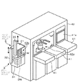
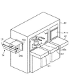
1、1a、1b
マルチストレージユニット
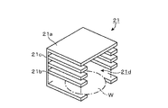
2 パージストレージユニット
3 ダミーストレージユニット
4 基板処理装置
5 回転部材
11 ユニットカバー
11a 排気口
12 排気手段
13 制御部
14 昇降機構
15 移動機構
21 パージストレージ
21a 天板
21b 保持部材
21c 背板
21d 開口部
22 昇降機構
31 ダミーストレージ
31a 隔壁
31b 保持部材
31d 開口部
32 昇降機構
41 ロードポート
41a 開閉ドア
42 ローダモジュール
42a 第1の基板搬送手段
42b 搬送口
43 ロードロック室
43a 載置台
44 トランスファモジュール
44a 第2の基板搬送手段
45a〜45d
処理モジュール
51 他のストレージ
52 縦板
52a 回転軸
53 底板
53a 通流口
53b 空洞
54 回転モータ
Claims (9)
- 搬入出ポートに載置されたキャリア内から搬送室内の基板搬送手段により基板を取り出して処理モジュールに受け渡し、この処理モジュール内にて基板の処理を行う基板処理装置において、
前記搬送室の外側に当該搬送室に連通するように搬送口を介して接続され、前記キャリアとは別に設けられた基板保管室と、
この基板保管室に設けられ、前記処理モジュールにて処理された後の基板上の反応生成物を吹き飛ばすためのパージガスの気流が形成されている雰囲気中にて、複数の基板を保管するための第1の保管棚と、
前記基板保管室に設けられ、複数のダミー基板を保管するための第2の保管棚と、
前記第1の保管棚及び第2の保管棚のうち選択された保管棚の基板保管領域を、前記基板搬送手段との間で前記搬送口を介して基板の受け渡しができるように位置させるために、当該第1の保管棚及び第2の保管棚を移動させる移動機構と、を備え、
前記基板保管室には、排気口が形成され、この排気口からパージガスが排気されることにより、第1の保管棚の基板保管領域にパージガスの気流が形成され、この第1の保管棚の基板保管領域を流れたパージガスの気流は、前記第2の保管棚の基板保管領域の外側を流れるように案内されることを特徴とする基板処理装置。 - 前記処理モジュールは真空雰囲気により処理が行われ、
前記搬送室は、搬入出ポートが接続される常圧雰囲気の常圧搬送室と、この常圧搬送室と前記処理モジュールとの間に介在する真空搬送室と、を備えると共にこれら常圧搬送室及び真空搬送室内に夫々基板搬送手段が設けられ、
前記基板保管室は、前記常圧搬送室に接続されていることを特徴とする請求項1に記載の基板処理装置。 - 第1の保管棚及び第2の保管棚は、互いに上下に配置され、前記移動機構は、これら保管棚を昇降させるように構成されていることを特徴とする請求項1または2に記載の基板処理装置。
- 前記移動機構は、前記第1の保管棚及び第2の保管棚を独立して昇降させるように構成されていることを特徴とする請求項3に記載の基板処理装置。
- 前記移動機構は、前記第1の保管棚及び第2の保管棚を連動して昇降させるように構成されていることを特徴とする請求項3に記載の基板処理装置。
- 前記第1の保管棚及び第2の保管棚は、前記搬送口から見て左右に直線状に配置され、前記移動機構は、これら保管棚を左右に移動させるように構成されていることを特徴とする請求項1または2に記載の基板処理装置。
- 前記第1の保管棚及び第2の保管棚は、鉛直軸周りに回転する回転部材に、前記鉛直軸の周りに沿って配置され、前記移動機構は、前記回転部材を回転させるように構成されていることを特徴とする請求項1または2に記載の基板処理装置。
- 搬入出ポートに載置されたキャリア内から搬送室内の基板搬送手段により基板を取り出して処理モジュールに受け渡し、この処理モジュール内にて基板の処理を行う基板処理方法において、
前記搬送室の外側に当該搬送室に連通するように搬送口を介して接続され、前記キャリアとは別に設けられた基板保管室内の第1の保管棚を、その基板保管領域が前記搬送口に臨むように移動機構により位置させる工程と、
次いで、前記基板搬送手段により前記搬送室内から基板を前記搬送口を介して前記第1の保管棚に受け渡し、前記処理モジュールにて処理された後の基板上の反応生成物を吹き飛ばすためのパージガスの気流が形成されている雰囲気中にて基板を保管する工程と、
前記基板保管室内の第2の保管棚を、その基板保管領域が前記搬送口に臨むように移動機構により位置させる工程と、
次いで、前記基板搬送手段により前記搬送室内からダミー基板を前記搬送口を介して前記第2の保管棚に受け渡し、ダミー基板を保管する工程と、
前記基板保管室に形成された排気口からパージガスが排気されることにより、第1の保管棚の基板保管領域にパージガスの気流を形成し、この第1の保管棚の基板保管領域を流れたパージガスの気流が、前記第2の保管棚の基板保管領域の外側を流れるように案内する工程と、を含むことを特徴とする基板処理方法。 - 搬入出ポートに載置されたキャリア内から搬送室内の基板搬送手段により基板を取り出して処理モジュールに受け渡し、この処理モジュール内にて基板の処理を行う基板処理装置において基板搬送装置に用いられるプログラムを格納した記憶媒体であって、
前記プログラムは請求項8に記載された基板処理方法を実行するためにステップが組まれていることを特徴とする記憶媒体。
Priority Applications (6)
| Application Number | Priority Date | Filing Date | Title |
|---|---|---|---|
| JP2007095376A JP4816545B2 (ja) | 2007-03-30 | 2007-03-30 | 基板処理装置、基板処理方法及び記憶媒体 |
| TW097111516A TW200849453A (en) | 2007-03-30 | 2008-03-28 | Substrate processing apparatus, substrate processing method and computer readable storage medium |
| PCT/JP2008/056082 WO2008120716A1 (ja) | 2007-03-30 | 2008-03-28 | 基板処理装置、基板処理方法及びコンピュータ可読記憶媒体 |
| CN2008800001223A CN101542713B (zh) | 2007-03-30 | 2008-03-28 | 基板处理装置和基板处理方法 |
| US12/532,190 US8382088B2 (en) | 2007-03-30 | 2008-03-28 | Substrate processing apparatus |
| KR1020087019754A KR101024530B1 (ko) | 2007-03-30 | 2008-03-28 | 기판 처리 장치, 기판 처리 방법 및, 컴퓨터 판독 가능 기억 매체 |
Applications Claiming Priority (1)
| Application Number | Priority Date | Filing Date | Title |
|---|---|---|---|
| JP2007095376A JP4816545B2 (ja) | 2007-03-30 | 2007-03-30 | 基板処理装置、基板処理方法及び記憶媒体 |
Publications (2)
| Publication Number | Publication Date |
|---|---|
| JP2008258188A JP2008258188A (ja) | 2008-10-23 |
| JP4816545B2 true JP4816545B2 (ja) | 2011-11-16 |
Family
ID=39808296
Family Applications (1)
| Application Number | Title | Priority Date | Filing Date |
|---|---|---|---|
| JP2007095376A Expired - Fee Related JP4816545B2 (ja) | 2007-03-30 | 2007-03-30 | 基板処理装置、基板処理方法及び記憶媒体 |
Country Status (6)
| Country | Link |
|---|---|
| US (1) | US8382088B2 (ja) |
| JP (1) | JP4816545B2 (ja) |
| KR (1) | KR101024530B1 (ja) |
| CN (1) | CN101542713B (ja) |
| TW (1) | TW200849453A (ja) |
| WO (1) | WO2008120716A1 (ja) |
Families Citing this family (30)
| Publication number | Priority date | Publication date | Assignee | Title |
|---|---|---|---|---|
| JP4816545B2 (ja) * | 2007-03-30 | 2011-11-16 | 東京エレクトロン株式会社 | 基板処理装置、基板処理方法及び記憶媒体 |
| GB2452320B (en) * | 2007-09-03 | 2012-04-11 | Dek Int Gmbh | Workpiece processing system and method |
| JP2010123733A (ja) * | 2008-11-19 | 2010-06-03 | Tokyo Electron Ltd | 基板処理装置及びその処理方法、並びに記憶媒体 |
| JP5410794B2 (ja) * | 2009-03-17 | 2014-02-05 | 東京エレクトロン株式会社 | 基板処理装置 |
| JP5358366B2 (ja) * | 2009-09-14 | 2013-12-04 | 東京エレクトロン株式会社 | 基板処理装置及び方法 |
| JP5947030B2 (ja) | 2010-12-28 | 2016-07-06 | キヤノンアネルバ株式会社 | 基板処理方法、基板処理装置 |
| KR101293025B1 (ko) * | 2011-12-22 | 2013-08-05 | 에스엔유 프리시젼 주식회사 | 마스크 적재 및 기판 반송 챔버와, 마스크 적재 및 기판 반송 챔버의 운용방법 |
| JP2013172015A (ja) * | 2012-02-21 | 2013-09-02 | Hitachi High-Technologies Corp | 成膜装置、及び成膜装置用基板搬送機構 |
| JP5959914B2 (ja) * | 2012-04-18 | 2016-08-02 | 東京エレクトロン株式会社 | 基板処理システム、基板搬送方法および記憶媒体 |
| JP2013247283A (ja) * | 2012-05-28 | 2013-12-09 | Tokyo Electron Ltd | 搬送機構、搬送方法及び処理システム |
| JP5954108B2 (ja) * | 2012-10-23 | 2016-07-20 | 東京エレクトロン株式会社 | 基板処理装置 |
| JP6016584B2 (ja) * | 2012-11-08 | 2016-10-26 | 東京エレクトロン株式会社 | ロードロック装置 |
| JP2014116545A (ja) * | 2012-12-12 | 2014-06-26 | Tokyo Electron Ltd | 基板処理装置 |
| KR101575129B1 (ko) * | 2014-01-13 | 2015-12-08 | 피에스케이 주식회사 | 기판 이송 장치 및 방법, 그리고 기판 처리 장치 |
| JP6494443B2 (ja) * | 2015-06-15 | 2019-04-03 | 東京エレクトロン株式会社 | 成膜方法及び成膜装置 |
| CN110770890B (zh) | 2017-06-23 | 2023-09-08 | 应用材料公司 | 可索引侧储存仓设备、加热的侧储存仓设备、系统和方法 |
| US10388547B2 (en) * | 2017-06-23 | 2019-08-20 | Applied Materials, Inc. | Side storage pods, equipment front end modules, and methods for processing substrates |
| KR102581283B1 (ko) * | 2017-10-11 | 2023-09-20 | 로제 가부시키가이샤 | 포드 오프너 |
| KR102110307B1 (ko) | 2018-04-23 | 2020-05-14 | 코스텍시스템(주) | 웨이퍼 이송 장치 |
| JP7349240B2 (ja) * | 2018-10-05 | 2023-09-22 | 東京エレクトロン株式会社 | 基板倉庫及び基板検査方法 |
| US11373891B2 (en) * | 2018-10-26 | 2022-06-28 | Applied Materials, Inc. | Front-ducted equipment front end modules, side storage pods, and methods of operating the same |
| US11244844B2 (en) * | 2018-10-26 | 2022-02-08 | Applied Materials, Inc. | High flow velocity, gas-purged, side storage pod apparatus, assemblies, and methods |
| CN109671658B (zh) * | 2018-11-29 | 2021-02-09 | 苏州方昇光电股份有限公司 | 基片装载系统及其基片装载方法 |
| KR102227066B1 (ko) | 2019-01-28 | 2021-03-15 | 코스텍시스템(주) | 웨이퍼 이송 장치 |
| JP7591370B2 (ja) * | 2020-08-28 | 2024-11-28 | 株式会社Screenホールディングス | 基板処理装置および基板処理方法 |
| CN113299586B (zh) * | 2021-07-28 | 2021-10-19 | 四川通妙科技有限公司 | 一种芯片晶圆暂存装置及芯片晶圆暂存取件方法 |
| TWI823271B (zh) * | 2022-02-24 | 2023-11-21 | 天虹科技股份有限公司 | 基板傳送方法 |
| JP7512520B2 (ja) * | 2022-03-15 | 2024-07-08 | 株式会社日立ハイテク | 真空処理装置 |
| JP7215629B1 (ja) | 2022-07-14 | 2023-01-31 | Jfeエンジニアリング株式会社 | バッテリ交換装置 |
| CN118016573B (zh) * | 2023-11-21 | 2025-06-20 | 唯实先端智能科技(苏州)有限公司 | 一种新型导流结构及高洁净晶圆光罩存储库 |
Family Cites Families (16)
| Publication number | Priority date | Publication date | Assignee | Title |
|---|---|---|---|---|
| JP2899192B2 (ja) * | 1993-03-03 | 1999-06-02 | 三菱マテリアルシリコン株式会社 | 半導体ウェーハの厚さ分類装置 |
| JPH06329208A (ja) * | 1993-05-20 | 1994-11-29 | Kokusai Electric Co Ltd | 半導体製造装置のウェーハ搬送装置 |
| JPH07117809A (ja) * | 1993-10-21 | 1995-05-09 | Ebara Corp | 真空保管庫 |
| JP2952748B2 (ja) * | 1994-11-24 | 1999-09-27 | 光洋リンドバーグ株式会社 | 熱処理装置 |
| US5944940A (en) * | 1996-07-09 | 1999-08-31 | Gamma Precision Technology, Inc. | Wafer transfer system and method of using the same |
| JPH11111810A (ja) * | 1997-10-07 | 1999-04-23 | Tokyo Electron Ltd | カセット室 |
| JPH11251255A (ja) * | 1998-02-27 | 1999-09-17 | Super Silicon Kenkyusho:Kk | 半導体ウエハ製造方法及び装置 |
| JP2002222844A (ja) * | 2001-01-24 | 2002-08-09 | Hitachi Kokusai Electric Inc | 半導体製造装置 |
| JP3920720B2 (ja) * | 2002-03-29 | 2007-05-30 | 株式会社荏原製作所 | 基板受渡し方法、基板受渡し機構及び基板研磨装置 |
| JP2004304116A (ja) * | 2003-04-01 | 2004-10-28 | Hitachi Kokusai Electric Inc | 基板処理装置 |
| EP1661161A2 (en) * | 2003-08-07 | 2006-05-31 | Sundew Technologies, LLC | Perimeter partition-valve with protected seals |
| JP4695936B2 (ja) * | 2005-07-15 | 2011-06-08 | 株式会社日立ハイテクノロジーズ | プラズマ処理装置 |
| JP4816545B2 (ja) * | 2007-03-30 | 2011-11-16 | 東京エレクトロン株式会社 | 基板処理装置、基板処理方法及び記憶媒体 |
| JP4987812B2 (ja) * | 2007-09-06 | 2012-07-25 | 株式会社日立国際電気 | 半導体装置の製造方法、基板処理方法及び基板処理装置 |
| JP2009170547A (ja) * | 2008-01-11 | 2009-07-30 | Tokyo Electron Ltd | 基板処理方法,基板処理装置,記録媒体 |
| JP4875190B2 (ja) * | 2009-08-31 | 2012-02-15 | 株式会社日立国際電気 | 基板処理装置及び半導体装置の製造方法 |
-
2007
- 2007-03-30 JP JP2007095376A patent/JP4816545B2/ja not_active Expired - Fee Related
-
2008
- 2008-03-28 US US12/532,190 patent/US8382088B2/en not_active Expired - Fee Related
- 2008-03-28 CN CN2008800001223A patent/CN101542713B/zh not_active Expired - Fee Related
- 2008-03-28 WO PCT/JP2008/056082 patent/WO2008120716A1/ja not_active Ceased
- 2008-03-28 TW TW097111516A patent/TW200849453A/zh not_active IP Right Cessation
- 2008-03-28 KR KR1020087019754A patent/KR101024530B1/ko not_active Expired - Fee Related
Also Published As
| Publication number | Publication date |
|---|---|
| CN101542713A (zh) | 2009-09-23 |
| TW200849453A (en) | 2008-12-16 |
| TWI379378B (ja) | 2012-12-11 |
| US8382088B2 (en) | 2013-02-26 |
| US20100102030A1 (en) | 2010-04-29 |
| CN101542713B (zh) | 2012-05-30 |
| WO2008120716A1 (ja) | 2008-10-09 |
| KR20090094054A (ko) | 2009-09-03 |
| KR101024530B1 (ko) | 2011-03-31 |
| JP2008258188A (ja) | 2008-10-23 |
Similar Documents
| Publication | Publication Date | Title |
|---|---|---|
| JP4816545B2 (ja) | 基板処理装置、基板処理方法及び記憶媒体 | |
| CN108933097B (zh) | 真空输送组件和基片处理装置 | |
| JP5503006B2 (ja) | 基板処理システム、搬送モジュール、基板処理方法及び半導体素子の製造方法 | |
| JP5212165B2 (ja) | 基板処理装置 | |
| KR102417929B1 (ko) | 기판 처리 장치 | |
| US8443513B2 (en) | Substrate processing apparatus | |
| CN110164794B (zh) | 基板输送装置和基板处理系统 | |
| JP6747136B2 (ja) | 基板処理装置 | |
| CN114570621A (zh) | 减压干燥装置 | |
| US20090087289A1 (en) | Structure for storing a substrate and semiconductor manufacturing apparatus | |
| JP5610009B2 (ja) | 基板処理装置 | |
| JP7624501B2 (ja) | 基板処理装置及び基板収納容器保管方法 | |
| US12603260B2 (en) | Apparatus for treating substrate and method for treating substrate | |
| US20110135427A1 (en) | Method for transferring target object and apparatus for processing target object | |
| KR20220023710A (ko) | 기판을 반송하는 장치, 기판을 처리하는 시스템, 및 기판을 처리하는 방법 | |
| KR20240061150A (ko) | 기판 반송 로봇 및 이를 포함하는 기판 처리 시스템 | |
| JP7521391B2 (ja) | 基板処理装置及び基板処理方法 | |
| JP7458212B2 (ja) | 基板搬送システムおよび基板搬送方法 | |
| JP7524736B2 (ja) | 基板処理装置、基板処理方法及び記憶媒体 | |
| JP7402658B2 (ja) | 基板収容ユニット及び基板搬送装置における真空搬送ユニットのメンテナンス方法 | |
| JP7316121B2 (ja) | 基板搬送装置及び基板搬送方法 | |
| KR20240122914A (ko) | 하이브리드 기판 본딩 시스템을 위한 foup 또는 카세트 저장소 | |
| JP7771609B2 (ja) | 基板処理装置及び基板処理方法 | |
| KR100781082B1 (ko) | 기판 반송 장치 및 그것을 사용한 기판 처리 설비 | |
| JP2005333076A (ja) | ロードロック装置、処理システム及びその使用方法 |
Legal Events
| Date | Code | Title | Description |
|---|---|---|---|
| A131 | Notification of reasons for refusal |
Free format text: JAPANESE INTERMEDIATE CODE: A131 Effective date: 20110125 |
|
| A521 | Request for written amendment filed |
Free format text: JAPANESE INTERMEDIATE CODE: A523 Effective date: 20110328 |
|
| TRDD | Decision of grant or rejection written | ||
| A01 | Written decision to grant a patent or to grant a registration (utility model) |
Free format text: JAPANESE INTERMEDIATE CODE: A01 Effective date: 20110802 |
|
| A01 | Written decision to grant a patent or to grant a registration (utility model) |
Free format text: JAPANESE INTERMEDIATE CODE: A01 |
|
| A61 | First payment of annual fees (during grant procedure) |
Free format text: JAPANESE INTERMEDIATE CODE: A61 Effective date: 20110815 |
|
| FPAY | Renewal fee payment (event date is renewal date of database) |
Free format text: PAYMENT UNTIL: 20140909 Year of fee payment: 3 |
|
| R150 | Certificate of patent or registration of utility model |
Free format text: JAPANESE INTERMEDIATE CODE: R150 |
|
| R250 | Receipt of annual fees |
Free format text: JAPANESE INTERMEDIATE CODE: R250 |
|
| LAPS | Cancellation because of no payment of annual fees |