JP5118923B2 - 半導体装置 - Google Patents
半導体装置 Download PDFInfo
- Publication number
- JP5118923B2 JP5118923B2 JP2007235269A JP2007235269A JP5118923B2 JP 5118923 B2 JP5118923 B2 JP 5118923B2 JP 2007235269 A JP2007235269 A JP 2007235269A JP 2007235269 A JP2007235269 A JP 2007235269A JP 5118923 B2 JP5118923 B2 JP 5118923B2
- Authority
- JP
- Japan
- Prior art keywords
- semiconductor device
- sensor element
- support frame
- integrated circuit
- lower container
- Prior art date
- Legal status (The legal status is an assumption and is not a legal conclusion. Google has not performed a legal analysis and makes no representation as to the accuracy of the status listed.)
- Expired - Fee Related
Links
- 239000004065 semiconductor Substances 0.000 title claims description 96
- 239000010410 layer Substances 0.000 claims description 58
- 230000001133 acceleration Effects 0.000 claims description 49
- XUIMIQQOPSSXEZ-UHFFFAOYSA-N Silicon Chemical compound [Si] XUIMIQQOPSSXEZ-UHFFFAOYSA-N 0.000 claims description 27
- 229910052710 silicon Inorganic materials 0.000 claims description 27
- 239000010703 silicon Substances 0.000 claims description 27
- 239000000758 substrate Substances 0.000 claims description 26
- 238000000034 method Methods 0.000 claims description 14
- 239000012790 adhesive layer Substances 0.000 claims description 5
- 238000005516 engineering process Methods 0.000 claims description 5
- 239000000956 alloy Substances 0.000 claims description 4
- 238000001514 detection method Methods 0.000 claims description 3
- 238000006073 displacement reaction Methods 0.000 claims description 3
- 229910000851 Alloy steel Inorganic materials 0.000 claims description 2
- IJGRMHOSHXDMSA-UHFFFAOYSA-N Atomic nitrogen Chemical compound N#N IJGRMHOSHXDMSA-UHFFFAOYSA-N 0.000 claims description 2
- 229910001111 Fine metal Inorganic materials 0.000 claims description 2
- 229910045601 alloy Inorganic materials 0.000 claims description 2
- 229910052782 aluminium Inorganic materials 0.000 claims description 2
- 239000000919 ceramic Substances 0.000 claims description 2
- 229910001873 dinitrogen Inorganic materials 0.000 claims description 2
- 229910052737 gold Inorganic materials 0.000 claims description 2
- 229920005989 resin Polymers 0.000 claims description 2
- 239000011347 resin Substances 0.000 claims description 2
- 239000010935 stainless steel Substances 0.000 claims description 2
- 229910001220 stainless steel Inorganic materials 0.000 claims description 2
- 229920001187 thermosetting polymer Polymers 0.000 claims description 2
- 238000005452 bending Methods 0.000 description 12
- 238000005530 etching Methods 0.000 description 9
- 238000004519 manufacturing process Methods 0.000 description 7
- 230000001681 protective effect Effects 0.000 description 5
- 238000001312 dry etching Methods 0.000 description 4
- 230000015572 biosynthetic process Effects 0.000 description 3
- 238000009792 diffusion process Methods 0.000 description 3
- 239000012535 impurity Substances 0.000 description 3
- 238000000059 patterning Methods 0.000 description 3
- 229910004298 SiO 2 Inorganic materials 0.000 description 2
- 239000010931 gold Substances 0.000 description 2
- 238000009616 inductively coupled plasma Methods 0.000 description 2
- 238000000206 photolithography Methods 0.000 description 2
- 238000003860 storage Methods 0.000 description 2
- VYPSYNLAJGMNEJ-UHFFFAOYSA-N Silicium dioxide Chemical compound O=[Si]=O VYPSYNLAJGMNEJ-UHFFFAOYSA-N 0.000 description 1
- XAGFODPZIPBFFR-UHFFFAOYSA-N aluminium Chemical compound [Al] XAGFODPZIPBFFR-UHFFFAOYSA-N 0.000 description 1
- 239000003822 epoxy resin Substances 0.000 description 1
- PCHJSUWPFVWCPO-UHFFFAOYSA-N gold Chemical compound [Au] PCHJSUWPFVWCPO-UHFFFAOYSA-N 0.000 description 1
- 239000012212 insulator Substances 0.000 description 1
- 238000010030 laminating Methods 0.000 description 1
- 238000012986 modification Methods 0.000 description 1
- 230000004048 modification Effects 0.000 description 1
- 230000001151 other effect Effects 0.000 description 1
- 229920000647 polyepoxide Polymers 0.000 description 1
- 229910052814 silicon oxide Inorganic materials 0.000 description 1
- 238000007740 vapor deposition Methods 0.000 description 1
Images







Classifications
-
- G—PHYSICS
- G01—MEASURING; TESTING
- G01P—MEASURING LINEAR OR ANGULAR SPEED, ACCELERATION, DECELERATION, OR SHOCK; INDICATING PRESENCE, ABSENCE, OR DIRECTION, OF MOVEMENT
- G01P15/00—Measuring acceleration; Measuring deceleration; Measuring shock, i.e. sudden change of acceleration
- G01P15/18—Measuring acceleration; Measuring deceleration; Measuring shock, i.e. sudden change of acceleration in two or more dimensions
-
- B—PERFORMING OPERATIONS; TRANSPORTING
- B81—MICROSTRUCTURAL TECHNOLOGY
- B81C—PROCESSES OR APPARATUS SPECIALLY ADAPTED FOR THE MANUFACTURE OR TREATMENT OF MICROSTRUCTURAL DEVICES OR SYSTEMS
- B81C1/00—Manufacture or treatment of devices or systems in or on a substrate
- B81C1/00015—Manufacture or treatment of devices or systems in or on a substrate for manufacturing microsystems
- B81C1/00222—Integrating an electronic processing unit with a micromechanical structure
- B81C1/00246—Monolithic integration, i.e. micromechanical structure and electronic processing unit are integrated on the same substrate
-
- G—PHYSICS
- G01—MEASURING; TESTING
- G01P—MEASURING LINEAR OR ANGULAR SPEED, ACCELERATION, DECELERATION, OR SHOCK; INDICATING PRESENCE, ABSENCE, OR DIRECTION, OF MOVEMENT
- G01P1/00—Details of instruments
- G01P1/02—Housings
- G01P1/023—Housings for acceleration measuring devices
-
- G—PHYSICS
- G01—MEASURING; TESTING
- G01P—MEASURING LINEAR OR ANGULAR SPEED, ACCELERATION, DECELERATION, OR SHOCK; INDICATING PRESENCE, ABSENCE, OR DIRECTION, OF MOVEMENT
- G01P15/00—Measuring acceleration; Measuring deceleration; Measuring shock, i.e. sudden change of acceleration
- G01P15/02—Measuring acceleration; Measuring deceleration; Measuring shock, i.e. sudden change of acceleration by making use of inertia forces using solid seismic masses
- G01P15/08—Measuring acceleration; Measuring deceleration; Measuring shock, i.e. sudden change of acceleration by making use of inertia forces using solid seismic masses with conversion into electric or magnetic values
- G01P15/0802—Details
-
- G—PHYSICS
- G01—MEASURING; TESTING
- G01P—MEASURING LINEAR OR ANGULAR SPEED, ACCELERATION, DECELERATION, OR SHOCK; INDICATING PRESENCE, ABSENCE, OR DIRECTION, OF MOVEMENT
- G01P15/00—Measuring acceleration; Measuring deceleration; Measuring shock, i.e. sudden change of acceleration
- G01P15/02—Measuring acceleration; Measuring deceleration; Measuring shock, i.e. sudden change of acceleration by making use of inertia forces using solid seismic masses
- G01P15/08—Measuring acceleration; Measuring deceleration; Measuring shock, i.e. sudden change of acceleration by making use of inertia forces using solid seismic masses with conversion into electric or magnetic values
- G01P15/12—Measuring acceleration; Measuring deceleration; Measuring shock, i.e. sudden change of acceleration by making use of inertia forces using solid seismic masses with conversion into electric or magnetic values by alteration of electrical resistance
- G01P15/123—Measuring acceleration; Measuring deceleration; Measuring shock, i.e. sudden change of acceleration by making use of inertia forces using solid seismic masses with conversion into electric or magnetic values by alteration of electrical resistance by piezo-resistive elements, e.g. semiconductor strain gauges
-
- B—PERFORMING OPERATIONS; TRANSPORTING
- B81—MICROSTRUCTURAL TECHNOLOGY
- B81B—MICROSTRUCTURAL DEVICES OR SYSTEMS, e.g. MICROMECHANICAL DEVICES
- B81B2201/00—Specific applications of microelectromechanical systems
- B81B2201/02—Sensors
- B81B2201/0228—Inertial sensors
- B81B2201/0235—Accelerometers
-
- B—PERFORMING OPERATIONS; TRANSPORTING
- B81—MICROSTRUCTURAL TECHNOLOGY
- B81C—PROCESSES OR APPARATUS SPECIALLY ADAPTED FOR THE MANUFACTURE OR TREATMENT OF MICROSTRUCTURAL DEVICES OR SYSTEMS
- B81C2203/00—Forming microstructural systems
- B81C2203/07—Integrating an electronic processing unit with a micromechanical structure
- B81C2203/0707—Monolithic integration, i.e. the electronic processing unit is formed on or in the same substrate as the micromechanical structure
- B81C2203/075—Monolithic integration, i.e. the electronic processing unit is formed on or in the same substrate as the micromechanical structure the electronic processing unit being integrated into an element of the micromechanical structure
-
- G—PHYSICS
- G01—MEASURING; TESTING
- G01P—MEASURING LINEAR OR ANGULAR SPEED, ACCELERATION, DECELERATION, OR SHOCK; INDICATING PRESENCE, ABSENCE, OR DIRECTION, OF MOVEMENT
- G01P15/00—Measuring acceleration; Measuring deceleration; Measuring shock, i.e. sudden change of acceleration
- G01P15/02—Measuring acceleration; Measuring deceleration; Measuring shock, i.e. sudden change of acceleration by making use of inertia forces using solid seismic masses
- G01P15/08—Measuring acceleration; Measuring deceleration; Measuring shock, i.e. sudden change of acceleration by making use of inertia forces using solid seismic masses with conversion into electric or magnetic values
- G01P2015/0805—Measuring acceleration; Measuring deceleration; Measuring shock, i.e. sudden change of acceleration by making use of inertia forces using solid seismic masses with conversion into electric or magnetic values being provided with a particular type of spring-mass-system for defining the displacement of a seismic mass due to an external acceleration
- G01P2015/0822—Measuring acceleration; Measuring deceleration; Measuring shock, i.e. sudden change of acceleration by making use of inertia forces using solid seismic masses with conversion into electric or magnetic values being provided with a particular type of spring-mass-system for defining the displacement of a seismic mass due to an external acceleration for defining out-of-plane movement of the mass
- G01P2015/084—Measuring acceleration; Measuring deceleration; Measuring shock, i.e. sudden change of acceleration by making use of inertia forces using solid seismic masses with conversion into electric or magnetic values being provided with a particular type of spring-mass-system for defining the displacement of a seismic mass due to an external acceleration for defining out-of-plane movement of the mass the mass being suspended at more than one of its sides, e.g. membrane-type suspension, so as to permit multi-axis movement of the mass
- G01P2015/0842—Measuring acceleration; Measuring deceleration; Measuring shock, i.e. sudden change of acceleration by making use of inertia forces using solid seismic masses with conversion into electric or magnetic values being provided with a particular type of spring-mass-system for defining the displacement of a seismic mass due to an external acceleration for defining out-of-plane movement of the mass the mass being suspended at more than one of its sides, e.g. membrane-type suspension, so as to permit multi-axis movement of the mass the mass being of clover leaf shape
Landscapes
- Physics & Mathematics (AREA)
- General Physics & Mathematics (AREA)
- Engineering & Computer Science (AREA)
- Manufacturing & Machinery (AREA)
- Microelectronics & Electronic Packaging (AREA)
- Pressure Sensors (AREA)
Description
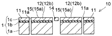
図1は、本発明の第1実施形態による半導体装置の平面図である。図2は、本発明の第1実施形態による半導体装置を簡略化して示した断面図である。図3は、本発明の第1実施形態による半導体装置の分解斜視図である。図4〜図6は、本発明の第1実施形態による半導体装置の構造を説明するための図である。まず、図1〜図6を参照して、本発明の第1実施形態による半導体装置50の構造について説明する。なお、図3ではボンディングワイヤなどの記載は省略している。
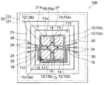
図11は、本発明の第2実施形態による半導体装置の平面図である。図12は、本発明の第2実施形態による半導体装置のセンサ素子の全体斜視図である。図13は、本発明の第2実施形態による半導体装置のセンサ素子の平面図である。次に、図11〜図13を参照して、本発明の第2実施形態による半導体装置100の構造について説明する。
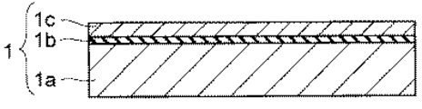
1a 支持基板
1b 絶縁層
1c シリコン層
1d、1e 上面領域
10、110 センサ素子
11 枠体部(支持枠)
12 重り部(構造体)
12a コア部(第1構造体)
12b 付随部(第2構造体)
13 撓み部(梁部)
14 ピエゾ抵抗素子
15、15a、15b 集積回路(集積回路部)
16 パッド電極(電極端子部)
20 パッケージ
21 下部容器
21a キャビティ
22 上部蓋
30 ボンディングワイヤ
50、100 半導体装置
111 連結部
112 配線層
Claims (33)
- 半導体プロセス技術を利用して形成されたシリコンからなるセンサ素子と、
前記センサ素子を収納するパッケージとを備え、
前記センサ素子は、支持枠と、前記支持枠の内側に配置される構造体と、前記構造体を前記支持枠に揺動可能に支持する梁部とを含み、
少なくとも前記構造体の上面領域の一部には、前記センサ素子と電気的に接続される集積回路部が形成されており、
前記構造体は、前記梁部を介して前記支持枠に支持される直方体状の第1構造体と、前記第1構造体に一体的に連結される直方体状の複数の第2構造体とを含み、
前記集積回路部は、前記複数の第2構造体の少なくとも1つの上面領域に形成されており、
前記支持枠の上面領域には、電極端子部が設けられているとともに、前記複数の第2構造体の一部と前記支持枠とは、連結部によって連結されており、
前記連結部は、前記支持枠の前記電極端子部と前記集積回路部とを電気的に接続するための接続経路として機能するように構成されており、
前記第2構造体のうちの1つの前記第2構造体の角部が、前記連結部によって支持枠の内側面と一体的に連結されており、
前記支持枠の所定領域および前記連結部の所定領域には、所定の配線パターンを有する配線層が形成されており、この配線層によって、前記集積回路部と前記電極端子部とが電気的に接続されていることを特徴とする、半導体装置。 - 前記センサ素子の前記梁部に、ピエゾ抵抗素子が形成されることによって、前記センサ素子が、前記構造体の変位量に応じて加速度を検出するピエゾ抵抗型の加速度センサ素子に構成されていることを特徴とする、請求項1に記載の半導体装置。
- 前記集積回路部は、前記第1構造体の上面領域および前記複数の第2構造体の上面領域の各々に形成されていることを特徴とする、請求項2に記載の半導体装置。
- 前記集積回路部は、前記構造体の上面領域に加えて、前記支持枠の上面領域にも形成されていることを特徴とする、請求項1〜2のいずれか1項に記載の半導体装置。
- 前記集積回路部は、前記構造体の動きに基づいて検出される電気的な検出信号を増幅および補正して、物理量に比例した電圧として出力する機能を有するように構成されていることを特徴とする、請求項1〜4のいずれか1項に記載の半導体装置。
- 前記支持枠、前記構造体および前記梁部は、SOI基板を加工することによって一体的に形成されていることを特徴とする、請求項1〜5のいずれか1項に記載の半導体装置。
- 前記センサ素子の前記支持枠は、平面的に見て、略矩形枠状に形成されており、中央部に略四角形状の開口部を有していることを特徴とする、請求項1〜6のいずれか1項に記載の半導体装置。
- 前記支持枠は、支持基板、絶縁層およびシリコン層から構成されていることを特徴とする、請求項1〜7のいずれか1項に記載の半導体装置。
- 前記第2構造体と前記支持枠および前記梁部との間には、隙間が設けられていることを特徴とする、請求項1〜8のいずれかを1項に記載の半導体装置。
- 前記隙間は、加速度を受けて構造体が揺動した際に、前記第2構造体が前記支持枠や前記梁部と接触しない程度の大きさに構成されていることを特徴とする、請求項9に記載の半導体装置。
- 前記梁部はSOI基板のシリコン層から構成されており、短冊状に形成されていることを特徴とする、請求項1〜10のいずれか1項に記載の半導体装置。
- 前記梁部は、前記支持枠よりも厚みが小さくなっていることを特徴とする、請求項1〜11のいずれか1項に記載の半導体装置。
- 前記梁部の一方端部が前記支持枠の内側面に一体的に連結されており、他方端部が前記構造体の内側面に一体的に連結されていることを特徴とする、請求項1〜12のいずれか1項に記載の半導体装置。
- 前記梁部は、所定の第1方向に延びるとともに前記第1構造体を挟む2つ1組の前記梁部と、前記第1方向と交差する第2方向に延びるとともに前記第1構造体を挟む2つ1組の前記梁部とに分けられることを特徴とする、請求項1〜13のいずれか1項に記載の半導体装置。
- 前記集積回路部は、ホイ―トストン・ブリッジ回路に構成された前記ピエゾ抵抗素子と配線層を介して電気的に接続されていることを特徴とする、請求項2〜14いずれか1項に記載の半導体装置。
- 前記電極端子部は、前記集積回路部によって増幅・補正された電気信号を外部に出力するための電極端子としての機能を有していることを特徴とする、請求項1〜15のいずれか1項に記載の半導体装置。
- 前記パッケージは、下部容器と上部蓋とから構成されていることを特徴とする、請求項1〜16のいずれか1項に記載の半導体装置。
- 前記下部容器は、積層構造を有するセラミック製の容器から構成されており、キャビティを有していることを特徴とする、請求項17に記載の半導体装置。
- 前記下部容器の側壁の前記キャビティ側には、前記下部容器の上面よりも低い段差面が形成されていることを特徴とする、請求項18に記載の半導体装置。
- 前記段差面にボンディングワイヤを介して、前記センサ素子の前記電極端子部と電気的に接続されるパッド電極が形成されていることを特徴とする、請求項19に記載の半導体装置。
- 前記下部容器の下面には、前記配線層と電気的に接続される電極端子が形成されていることを特徴とする、請求項17〜20のいずれか1項に記載の半導体装置。
- 前記電極端子と前記パッド電極とは、前記下部容器内部に形成された配線部を介して、互いに電気的に接続されていることを特徴とする、請求項21に記載の半導体装置。
- 前記センサ素子は、前記下部容器のキャビティの底面における中央部の領域に接着層を介して固着されていることを特徴とする、請求項1〜22のいずれか1項に記載の半導体装置。
- 前記下部容器の前記キャビティの底面と前記センサ素子との間には、隙間部が形成されていることを特徴とする、請求項18〜23のいずれか1項に記載の半導体装置。
- 前記隙間部が50μm〜100μmの高さを有することを特徴とする、請求項24に記載の半導体装置。
- 前記ボンディングワイヤはAuまたはAlからなる金属細線から構成されていることを特徴とする、請求項20〜25のいずれか1項に記載の半導体装置。
- 前記キャビティは、前記上部蓋によって封止されていることを特徴とする、請求項18〜20のいずれか1項に記載の半導体装置。
- 前記上部蓋は、熱硬化性樹脂からなる接着層によって、前記下部容器の前記キャビティを密閉するように前記下部容器の上面に固着されていることを特徴とする、請求項17〜27のいずれか1項に記載の半導体装置。
- 前記上部蓋は、42アロイ合金またはステンレスから構成されていることを特徴とする、請求項17〜28のいずれか1項に記載の半導体装置。
- 前記パッケージの内部は、窒素ガスまたはドライエアーでパージされていることを特徴とする、請求項1〜29のいずれか1項に記載の半導体装置。
- 前記連結部はシリコン層を含むように構成されていることを特徴とする、請求項1〜30のいずれか1項に記載の半導体装置。
- 前記センサ素子は、3軸方向の加速度を検出する3軸加速度センサ素子、2軸方向の加速度を検出する2軸加速度センサ素子、または、1軸方向の加速度を検出する1軸加速度センサ素子のいずれかであることを特徴とする、請求項1〜31のいずれか1項に記載の半導体装置。
- 前記センサ素子全体がSOI基板から構成されていることを特徴とする、請求項1〜32のいずれか1項に記載の半導体装置。
Priority Applications (2)
| Application Number | Priority Date | Filing Date | Title |
|---|---|---|---|
| JP2007235269A JP5118923B2 (ja) | 2007-09-11 | 2007-09-11 | 半導体装置 |
| PCT/JP2008/065652 WO2009034863A1 (ja) | 2007-09-11 | 2008-09-01 | 半導体装置 |
Applications Claiming Priority (1)
| Application Number | Priority Date | Filing Date | Title |
|---|---|---|---|
| JP2007235269A JP5118923B2 (ja) | 2007-09-11 | 2007-09-11 | 半導体装置 |
Publications (3)
| Publication Number | Publication Date |
|---|---|
| JP2009068893A JP2009068893A (ja) | 2009-04-02 |
| JP2009068893A5 JP2009068893A5 (ja) | 2010-10-14 |
| JP5118923B2 true JP5118923B2 (ja) | 2013-01-16 |
Family
ID=40451872
Family Applications (1)
| Application Number | Title | Priority Date | Filing Date |
|---|---|---|---|
| JP2007235269A Expired - Fee Related JP5118923B2 (ja) | 2007-09-11 | 2007-09-11 | 半導体装置 |
Country Status (2)
| Country | Link |
|---|---|
| JP (1) | JP5118923B2 (ja) |
| WO (1) | WO2009034863A1 (ja) |
Families Citing this family (2)
| Publication number | Priority date | Publication date | Assignee | Title |
|---|---|---|---|---|
| KR101071915B1 (ko) | 2009-07-06 | 2011-10-11 | 주식회사 이노칩테크놀로지 | 가속도 센서 및 이의 제조 방법 |
| KR101132263B1 (ko) | 2010-01-08 | 2012-04-02 | 주식회사 이노칩테크놀로지 | 가속도 센싱 조립체와 그 제작 방법 |
Family Cites Families (5)
| Publication number | Priority date | Publication date | Assignee | Title |
|---|---|---|---|---|
| JP2505987Y2 (ja) * | 1989-12-28 | 1996-08-07 | 株式会社ワコー | 加速度センサ |
| JP3478894B2 (ja) * | 1995-02-20 | 2003-12-15 | 株式会社東海理化電機製作所 | 表面型の加速度センサ |
| JPH08327657A (ja) * | 1995-06-01 | 1996-12-13 | Nikon Corp | 力学量センサ |
| JP2007035965A (ja) * | 2005-07-27 | 2007-02-08 | Oki Electric Ind Co Ltd | 半導体装置およびその製造方法、ならびにそれに使用される接着材料およびその製造方法 |
| JP3938202B1 (ja) * | 2006-03-28 | 2007-06-27 | 松下電工株式会社 | センサパッケージの製造方法 |
-
2007
- 2007-09-11 JP JP2007235269A patent/JP5118923B2/ja not_active Expired - Fee Related
-
2008
- 2008-09-01 WO PCT/JP2008/065652 patent/WO2009034863A1/ja not_active Ceased
Also Published As
| Publication number | Publication date |
|---|---|
| JP2009068893A (ja) | 2009-04-02 |
| WO2009034863A1 (ja) | 2009-03-19 |
Similar Documents
| Publication | Publication Date | Title |
|---|---|---|
| JP5486271B2 (ja) | 加速度センサ、及び加速度センサの製造方法 | |
| KR100985453B1 (ko) | 센서 장치 및 그 제조 방법 | |
| JP4670427B2 (ja) | 半導体センサおよびその製造方法 | |
| JP4754817B2 (ja) | 半導体加速度センサ | |
| JP6468167B2 (ja) | 力学量センサ | |
| JP6209270B2 (ja) | 加速度センサ | |
| JP2006170856A (ja) | 加速度センサ | |
| JP5118923B2 (ja) | 半導体装置 | |
| JP2005127750A (ja) | 半導体センサおよびその製造方法 | |
| JP4428210B2 (ja) | 物理量センサの実装構造 | |
| JP5167848B2 (ja) | 支持基板及びそれを用いた静電容量型力学量検出センサの製造方法 | |
| JP6464770B2 (ja) | 物理量センサおよびその製造方法 | |
| JP3938199B1 (ja) | ウェハレベルパッケージ構造体およびセンサ装置 | |
| CN101317262A (zh) | 传感器装置及其制造方法 | |
| JP3938205B1 (ja) | センサエレメント | |
| JP2008122304A (ja) | 静電容量式加速度センサ | |
| JP4466344B2 (ja) | 加速度センサ | |
| JP4706634B2 (ja) | 半導体センサおよびその製造方法 | |
| JP4665733B2 (ja) | センサエレメント | |
| JP5678535B2 (ja) | 力学量センサ及び力学量センサの製造方法 | |
| JP4000170B2 (ja) | チップサイズパッケージ | |
| JP5069410B2 (ja) | センサエレメント | |
| JP3938200B1 (ja) | センサ装置およびその製造方法 | |
| JP2016170100A (ja) | シリコン配線埋め込みガラス基板およびそれを用いたセンサ | |
| JP2007263767A (ja) | センサ装置 |
Legal Events
| Date | Code | Title | Description |
|---|---|---|---|
| A521 | Written amendment |
Free format text: JAPANESE INTERMEDIATE CODE: A523 Effective date: 20100830 |
|
| A621 | Written request for application examination |
Free format text: JAPANESE INTERMEDIATE CODE: A621 Effective date: 20100831 |
|
| A131 | Notification of reasons for refusal |
Free format text: JAPANESE INTERMEDIATE CODE: A131 Effective date: 20120703 |
|
| A521 | Written amendment |
Free format text: JAPANESE INTERMEDIATE CODE: A523 Effective date: 20120829 |
|
| TRDD | Decision of grant or rejection written | ||
| A01 | Written decision to grant a patent or to grant a registration (utility model) |
Free format text: JAPANESE INTERMEDIATE CODE: A01 Effective date: 20120925 |
|
| A01 | Written decision to grant a patent or to grant a registration (utility model) |
Free format text: JAPANESE INTERMEDIATE CODE: A01 |
|
| A61 | First payment of annual fees (during grant procedure) |
Free format text: JAPANESE INTERMEDIATE CODE: A61 Effective date: 20121022 |
|
| R150 | Certificate of patent or registration of utility model |
Ref document number: 5118923 Country of ref document: JP Free format text: JAPANESE INTERMEDIATE CODE: R150 Free format text: JAPANESE INTERMEDIATE CODE: R150 |
|
| FPAY | Renewal fee payment (event date is renewal date of database) |
Free format text: PAYMENT UNTIL: 20151026 Year of fee payment: 3 |
|
| R250 | Receipt of annual fees |
Free format text: JAPANESE INTERMEDIATE CODE: R250 |
|
| RD03 | Notification of appointment of power of attorney |
Free format text: JAPANESE INTERMEDIATE CODE: R3D03 |
|
| LAPS | Cancellation because of no payment of annual fees |