JP5219324B2 - 温度補償型単一電源hfet - Google Patents
温度補償型単一電源hfet Download PDFInfo
- Publication number
- JP5219324B2 JP5219324B2 JP2001581347A JP2001581347A JP5219324B2 JP 5219324 B2 JP5219324 B2 JP 5219324B2 JP 2001581347 A JP2001581347 A JP 2001581347A JP 2001581347 A JP2001581347 A JP 2001581347A JP 5219324 B2 JP5219324 B2 JP 5219324B2
- Authority
- JP
- Japan
- Prior art keywords
- field effect
- schottky diode
- effect transistor
- stack
- layer
- Prior art date
- Legal status (The legal status is an assumption and is not a legal conclusion. Google has not performed a legal analysis and makes no representation as to the accuracy of the status listed.)
- Expired - Fee Related
Links
Images



Classifications
-
- H—ELECTRICITY
- H10—SEMICONDUCTOR DEVICES; ELECTRIC SOLID-STATE DEVICES NOT OTHERWISE PROVIDED FOR
- H10D—INORGANIC ELECTRIC SEMICONDUCTOR DEVICES
- H10D84/00—Integrated devices formed in or on semiconductor substrates that comprise only semiconducting layers, e.g. on Si wafers or on GaAs-on-Si wafers
- H10D84/01—Manufacture or treatment
- H10D84/02—Manufacture or treatment characterised by using material-based technologies
- H10D84/05—Manufacture or treatment characterised by using material-based technologies using Group III-V technology
-
- H—ELECTRICITY
- H03—ELECTRONIC CIRCUITRY
- H03F—AMPLIFIERS
- H03F1/00—Details of amplifiers with only discharge tubes, only semiconductor devices or only unspecified devices as amplifying elements
- H03F1/30—Modifications of amplifiers to reduce influence of variations of temperature or supply voltage or other physical parameters
- H03F1/301—Modifications of amplifiers to reduce influence of variations of temperature or supply voltage or other physical parameters in MOSFET amplifiers
-
- H—ELECTRICITY
- H03—ELECTRONIC CIRCUITRY
- H03K—PULSE TECHNIQUE
- H03K17/00—Electronic switching or gating, i.e. not by contact-making and –breaking
- H03K17/14—Modifications for compensating variations of physical values, e.g. of temperature
- H03K17/145—Modifications for compensating variations of physical values, e.g. of temperature in field-effect transistor switches
-
- H—ELECTRICITY
- H10—SEMICONDUCTOR DEVICES; ELECTRIC SOLID-STATE DEVICES NOT OTHERWISE PROVIDED FOR
- H10D—INORGANIC ELECTRIC SEMICONDUCTOR DEVICES
- H10D84/00—Integrated devices formed in or on semiconductor substrates that comprise only semiconducting layers, e.g. on Si wafers or on GaAs-on-Si wafers
- H10D84/01—Manufacture or treatment
-
- H—ELECTRICITY
- H10—SEMICONDUCTOR DEVICES; ELECTRIC SOLID-STATE DEVICES NOT OTHERWISE PROVIDED FOR
- H10D—INORGANIC ELECTRIC SEMICONDUCTOR DEVICES
- H10D84/00—Integrated devices formed in or on semiconductor substrates that comprise only semiconducting layers, e.g. on Si wafers or on GaAs-on-Si wafers
- H10D84/01—Manufacture or treatment
- H10D84/0107—Integrating at least one component covered by H10D12/00 or H10D30/00 with at least one component covered by H10D8/00, H10D10/00 or H10D18/00, e.g. integrating IGFETs with BJTs
-
- H—ELECTRICITY
- H10—SEMICONDUCTOR DEVICES; ELECTRIC SOLID-STATE DEVICES NOT OTHERWISE PROVIDED FOR
- H10D—INORGANIC ELECTRIC SEMICONDUCTOR DEVICES
- H10D89/00—Aspects of integrated devices not covered by groups H10D84/00 - H10D88/00
- H10D89/60—Integrated devices comprising arrangements for electrical or thermal protection, e.g. protection circuits against electrostatic discharge [ESD]
Landscapes
- Engineering & Computer Science (AREA)
- Power Engineering (AREA)
- Junction Field-Effect Transistors (AREA)
- Electrodes Of Semiconductors (AREA)
Description
技術分野
本発明は、単一電源を用いた温度補償HFETの装置及び方法に関する。
従来技術の説明
電力増幅器等など最近の通信電子機器は、高効率、高性能、かつ低電流ドレインの出力半導体デバイスを必要とする。エンハンスメント型ヘテロ接合電界効果トランジスタ(HFET)は、単一電源、即ち単一極性の電源で動作可能である。また、かかるデバイス技術においては幅広い温度にわたってデバイス動作を安定化させる自己バイアス能力が得られることが望ましく、有利である。pn接合、即ちHFETプロセスに統合されたショットキ・ダイオードは、この要望を満たすことが可能である。しかしながら、pn接合ダイオードは、1電子ボルトを超えるポテンシャル障壁を有しており、約3ボルトのドレイン供給電圧を有する低電圧電力増幅器にするには高すぎる。ターン・オン電圧は好適には約0.6ボルト以下である。
したがって、高い温度係数、及び低いターン・オン電圧で温度補償を行う装置及び方法を提供することは極めて望ましいことである。
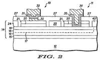
図2を参照する。本発明により同一工程で製造されたヘテロ接合電界効果トランジスタ(HFET)10、及び隣接するショットキ・ダイオード11を簡略断面図が示されている。この特定の実施形態においては、単なる説明の目的から、HFETはRF増幅器用に使用されるべく設計された非常に大きなRFデバイス(例えば、数アンペアの電流を流し得る40mmのデバイス)であり、ショットキ・ダイオード11はHFET10よりも極めて小さい大きさであって極小量の電流を流す。HFET10及びショットキ・ダイオード11の製造において、基板12は、その上面にエピタキシャル成長させた化合物半導体層のスタック14を有する。種々の化合物半導体材料を用いてHFET10を形成することが可能であることは理解されるであろうが、この特定実施形態では、基板12はバッファ15を備えたガリウム砒素(GaAs)ウエハである。このバッファ15は、基板12の上面にて使用される工程、及び形成される材料に応じて、1つ以上の層とすることができる。GaAsの層16をバッファ15上に成長させ、シリコンδドーピングの薄い層17を層16上に堆積させる。GaAsの第2層18を層17上に成長させ、砒化ガリウム・インジウム(InGaAs)のチャネル層19を層18上に成長させる。砒化アルミニウムガリウム(AlGaAs)の層20をチャネル層19上に成長させ、GaAsのキャップ層21を層20上に成長させスタック14を完成させる。
Claims (5)
- 上面に形成されたエピタキシャル成長の複数の化合物半導体層のスタックを有する基板と、同スタックは第1エピタキシャル成長化合物半導体層を有することと、
前記スタックの前記第1エピタキシャル成長化合物半導体層を有する少なくとも第1部分に形成されるとともに、ソース及びドレインとのオーミック・コンタクトを備えたチャネルと該チャネルと動作的に対応するゲート接続とを有したヘテロ接合電界効果トランジスタと、前記ゲート接続は複数の金属層を積層してなることと、前記ヘテロ接合電界効果トランジスタは第1のターン・オン電圧を有することと、
前記ヘテロ電界効果トランジスタに隣接させて前記スタックの前記第1エピタキシャル成長化合物半導体層を有する少なくとも第2部分に形成されるショットキ・ダイオードと、同ショットキ・ダイオードは前記ヘテロ接合電界効果トランジスタに隣接し、かつ前記ショットキ・ダイオードは2つの端子を有することと、同ショットキ・ダイオードは、前記スタックのうちで最も低いバンドギャップを有する層に接触して前記複数の金属層を積層してなる層を有することと、同ショットキ・ダイオードは負の温度係数と前記第1ターン・オン電圧よりも低い第2ターン・オン電圧とを有することとからなり、単一電源に接続された前記ショットキ・ダイオードと前記へテロ電界効果トランジスタを互いに隣接して設けることによって、前記ヘテロ接合電界効果トランジスタ内で1.8V以下の低電圧の温度補償を行う、装置。
- 前記ヘテロ接合電界効果トランジスタは負の温度係数を有し、前記ショットキ・ダイオードは温度変化に伴う前記ゲート回路内の電流負荷の変化を補償すべくゲート回路によって前記ヘテロ接合電界効果トランジスタの前記ゲート接続に接続される、請求項1記載の装置。
- 第1エピタキシャル成長化合物半導体層を有するエピタキシャル成長化合物半導体層スタックが上面に形成された基板を提供する工程と、
ソース及びドレインとのオーミック・コンタクトを備えたチャネルと、複数の金属層を積層してなる層からなるゲート接続であって前記チャネルに動作的に対応させたゲート接続とが形成され、第1ターン・オン電圧を有したヘテロ接合電界効果トランジスタを前記スタックの前記第1エピタキシャル成長化合物半導体層を有した第1部分に少なくとも形成する工程と、
前記スタックの前記エピタキシャル成長化合物半導体層を有した少なくとも第2部分に、二つの端子を備えたショットキ・ダイオードであって、前記スタックのうちで最も低いバンドギャップを有する層に接触して前記複数の金属層を積層してなる層を有するとともに負の温度係数を有したショットキ・ダイオードを前記ヘテロ接合電界効果トランジスタに隣接して形成する工程とからなる、単一電源の前記ショットキ・ダイオードと前記へテロ電界効果トランジスタを互いに隣接して設けることによって、前記ヘテロ接合電界効果トランジスタ内で1.8V以下の低電圧の温度補償を行う装置の製造方法。
- 前記ショットキ・ダイオードを形成する工程は、前記ヘテロ接合電界効果トランジスタの前記ゲート接続及び前記ショットキ・ダイオードと同時に前記複数の金属層を積層してなる層を堆積することによって行われる、請求項3記載の製造方法。
- 前記ヘテロ接合電界効果トランジスタは負の温度係数を有し、前記方法は、温度変化に伴う前記ゲート回路内の電流負荷の変化を補償すべく前記ショットキ・ダイオードをゲート回路によって前記ヘテロ接合電界効果トランジスタのゲート接続に接続する工程をさらに有する請求項3記載の製造方法。
Applications Claiming Priority (3)
| Application Number | Priority Date | Filing Date | Title |
|---|---|---|---|
| US09/559,791 | 2000-04-27 | ||
| US09/559,791 US6479843B2 (en) | 2000-04-27 | 2000-04-27 | Single supply HFET with temperature compensation |
| PCT/US2001/011921 WO2001084630A1 (en) | 2000-04-27 | 2001-04-11 | Single supply hfet with temperature compensation |
Publications (3)
| Publication Number | Publication Date |
|---|---|
| JP2003533027A JP2003533027A (ja) | 2003-11-05 |
| JP2003533027A5 JP2003533027A5 (ja) | 2008-06-05 |
| JP5219324B2 true JP5219324B2 (ja) | 2013-06-26 |
Family
ID=24235037
Family Applications (1)
| Application Number | Title | Priority Date | Filing Date |
|---|---|---|---|
| JP2001581347A Expired - Fee Related JP5219324B2 (ja) | 2000-04-27 | 2001-04-11 | 温度補償型単一電源hfet |
Country Status (7)
| Country | Link |
|---|---|
| US (1) | US6479843B2 (ja) |
| JP (1) | JP5219324B2 (ja) |
| KR (1) | KR100708228B1 (ja) |
| CN (1) | CN1249813C (ja) |
| AU (1) | AU2001251572A1 (ja) |
| TW (1) | TW503576B (ja) |
| WO (1) | WO2001084630A1 (ja) |
Families Citing this family (20)
| Publication number | Priority date | Publication date | Assignee | Title |
|---|---|---|---|---|
| US6690042B2 (en) * | 2000-09-27 | 2004-02-10 | Sensor Electronic Technology, Inc. | Metal oxide semiconductor heterostructure field effect transistor |
| JP4469139B2 (ja) * | 2003-04-28 | 2010-05-26 | シャープ株式会社 | 化合物半導体fet |
| US7253015B2 (en) * | 2004-02-17 | 2007-08-07 | Velox Semiconductor Corporation | Low doped layer for nitride-based semiconductor device |
| JP4866007B2 (ja) * | 2005-01-14 | 2012-02-01 | 富士通株式会社 | 化合物半導体装置 |
| US7504677B2 (en) * | 2005-03-28 | 2009-03-17 | Freescale Semiconductor, Inc. | Multi-gate enhancement mode RF switch and bias arrangement |
| ATE457525T1 (de) * | 2005-11-28 | 2010-02-15 | Nxp Bv | Verfahren zur herstellung selbstausgerichteter schottky-dioden für halbleiterbauelemente |
| WO2007108017A1 (en) * | 2006-03-20 | 2007-09-27 | Stmicroelectronics S.R.L. | Semiconductor field-effect transistor, memory cell and memory device |
| US7701031B2 (en) * | 2006-04-07 | 2010-04-20 | United Microelectronics Corp. | Integrated circuit structure and manufacturing method thereof |
| DE102006018765A1 (de) * | 2006-04-20 | 2007-10-25 | Infineon Technologies Ag | Leistungshalbleiterbauelement, Leistungshalbleiterbauteil sowie Verfahren zu deren Herstellung |
| US7915704B2 (en) * | 2009-01-26 | 2011-03-29 | Freescale Semiconductor, Inc. | Schottky diode |
| JP2011082216A (ja) * | 2009-10-02 | 2011-04-21 | Fujitsu Ltd | 化合物半導体装置及びその製造方法 |
| US8368121B2 (en) * | 2010-06-21 | 2013-02-05 | Power Integrations, Inc. | Enhancement-mode HFET circuit arrangement having high power and high threshold voltage |
| CN102194819A (zh) * | 2011-04-26 | 2011-09-21 | 电子科技大学 | 一种基于MOS控制的增强型GaN异质结场效应晶体管 |
| TWI508281B (zh) * | 2011-08-01 | 2015-11-11 | Murata Manufacturing Co | Field effect transistor |
| JP5662367B2 (ja) * | 2012-03-26 | 2015-01-28 | 株式会社東芝 | 窒化物半導体装置およびその製造方法 |
| KR102127441B1 (ko) * | 2013-12-02 | 2020-06-26 | 엘지이노텍 주식회사 | 반도체 소자 및 이를 포함하는 반도체 회로 |
| KR102182016B1 (ko) | 2013-12-02 | 2020-11-23 | 엘지이노텍 주식회사 | 반도체 소자 및 이를 포함하는 반도체 회로 |
| EP2922093B1 (en) * | 2014-03-19 | 2017-05-10 | Nxp B.V. | Hemt temperature sensor |
| KR101559111B1 (ko) | 2014-04-10 | 2015-10-13 | 홍익대학교 산학협력단 | 양방향 스위칭 소자 및 그 제조 방법 |
| CN112187237B (zh) * | 2020-09-29 | 2021-12-21 | 西安博瑞集信电子科技有限公司 | 一种使能电路 |
Family Cites Families (13)
| Publication number | Priority date | Publication date | Assignee | Title |
|---|---|---|---|---|
| EP0206274B1 (en) | 1985-06-21 | 1991-10-23 | Honeywell Inc. | High transconductance complementary ic structure |
| US4760288A (en) * | 1986-07-21 | 1988-07-26 | Honeywell Inc. | Temperature compensation for semiconductor logic gates |
| JPH01251819A (ja) * | 1988-03-30 | 1989-10-06 | Nec Corp | Bfl回路 |
| JPH03228365A (ja) * | 1990-02-02 | 1991-10-09 | Sumitomo Electric Ind Ltd | 半導体抵抗回路 |
| JP2786307B2 (ja) * | 1990-04-19 | 1998-08-13 | 三菱電機株式会社 | 電界効果トランジスタ及びその製造方法 |
| US5341114A (en) * | 1990-11-02 | 1994-08-23 | Ail Systems, Inc. | Integrated limiter and amplifying devices |
| DE4219523A1 (de) * | 1992-06-15 | 1993-12-16 | Daimler Benz Ag | Monolithisch integrierter Millimeterwellenschaltkreis und Verfahren zu dessen Herstellung |
| JPH07106525A (ja) * | 1993-10-01 | 1995-04-21 | Hitachi Ltd | 電界効果トランジスタおよび化合物半導体集積回路 |
| EP0710984B1 (en) * | 1994-11-02 | 2001-08-08 | Trw Inc. | Method of fabricating monolithic multifunction integrated circuit devices |
| US5532486A (en) * | 1995-02-13 | 1996-07-02 | Hughes Aircraft Company | Heterojunction diode with low turn-on voltage |
| JP2669394B2 (ja) * | 1995-02-16 | 1997-10-27 | 日本電気株式会社 | 電界効果型トランジスタ |
| JPH08250670A (ja) * | 1995-03-08 | 1996-09-27 | Oki Electric Ind Co Ltd | 半導体装置 |
| JP3379062B2 (ja) * | 1997-12-02 | 2003-02-17 | 富士通カンタムデバイス株式会社 | 半導体装置及びその製造方法 |
-
2000
- 2000-04-27 US US09/559,791 patent/US6479843B2/en not_active Expired - Lifetime
-
2001
- 2001-04-11 KR KR20027014444A patent/KR100708228B1/ko not_active Expired - Fee Related
- 2001-04-11 WO PCT/US2001/011921 patent/WO2001084630A1/en not_active Ceased
- 2001-04-11 JP JP2001581347A patent/JP5219324B2/ja not_active Expired - Fee Related
- 2001-04-11 CN CNB018086756A patent/CN1249813C/zh not_active Expired - Lifetime
- 2001-04-11 AU AU2001251572A patent/AU2001251572A1/en not_active Abandoned
- 2001-04-26 TW TW090109999A patent/TW503576B/zh not_active IP Right Cessation
Also Published As
| Publication number | Publication date |
|---|---|
| KR20020093089A (ko) | 2002-12-12 |
| US20020127787A1 (en) | 2002-09-12 |
| CN1452789A (zh) | 2003-10-29 |
| CN1249813C (zh) | 2006-04-05 |
| JP2003533027A (ja) | 2003-11-05 |
| WO2001084630A1 (en) | 2001-11-08 |
| KR100708228B1 (ko) | 2007-04-17 |
| TW503576B (en) | 2002-09-21 |
| AU2001251572A1 (en) | 2001-11-12 |
| US6479843B2 (en) | 2002-11-12 |
Similar Documents
| Publication | Publication Date | Title |
|---|---|---|
| JP5219324B2 (ja) | 温度補償型単一電源hfet | |
| US10158029B2 (en) | Apparatus and methods for robust overstress protection in compound semiconductor circuit applications | |
| US6521961B1 (en) | Semiconductor device using a barrier layer between the gate electrode and substrate and method therefor | |
| US20110210337A1 (en) | Monolithic integration of silicon and group III-V devices | |
| US7952150B1 (en) | Enhancement mode MOSFET and depletion mode FET on a common group III-V substrate | |
| US12074159B2 (en) | Nitride-based semiconductor bidirectional switching device and method for manufacturing the same | |
| US12317587B2 (en) | Apparatus and circuits including transistors with different threshold voltages and methods of fabricating the same | |
| US20220130989A1 (en) | Apparatus and circuits including transistors with different polarizations and methods of fabricating the same | |
| US6365925B2 (en) | Semiconductor device | |
| US20250176253A1 (en) | Group iii-v ic with different sheet resistance 2-deg resistors | |
| US11990541B2 (en) | Apparatus and circuits with dual polarization transistors and methods of fabricating the same | |
| US5610410A (en) | III-V compound semiconductor device with Schottky electrode of increased barrier height | |
| CN107039427A (zh) | 半导体器件 | |
| Leuther et al. | InGaAs HEMT MMIC technology on silicon substrate with backside field-plate | |
| US20250294864A1 (en) | Compound semiconductor device for high power and high frequency operation | |
| US6919590B2 (en) | Heterojunction bipolar transistor with monolithically integrated junction field effect transistor and method of manufacturing same | |
| US20250159982A1 (en) | Apparatus and circuits with dual threshold voltage transistors and methods of fabricating the same | |
| KR101873219B1 (ko) | 질화갈륨계 전력 스위칭 장치 | |
| US20250096582A1 (en) | Circuitry connecting to battery, regulation circuit and method thereof | |
| US20260019050A1 (en) | Compensated amplifier circuit | |
| US20250096558A1 (en) | Semiconductor device structure and method of manufacturing the same | |
| WO1999027586A2 (en) | INxGa1-xP STOP-ETCH LAYER FOR SELECTIVE RECESS OF GALLIUM ARSENIDE-BASED EPTITAXIAL FIELD EFFECT TRANSISTORS AND PROCESS THEREFOR | |
| CN121888630A (zh) | 用于使用二维电子气的晶体管结构的正导通和负截止衬底偏置 | |
| JPS62219671A (ja) | 砒化ガリウム半導体装置 | |
| JP2001274326A (ja) | リーク電流抑制方法 |
Legal Events
| Date | Code | Title | Description |
|---|---|---|---|
| A711 | Notification of change in applicant |
Free format text: JAPANESE INTERMEDIATE CODE: A711 Effective date: 20040927 |
|
| A521 | Request for written amendment filed |
Free format text: JAPANESE INTERMEDIATE CODE: A523 Effective date: 20080411 |
|
| A621 | Written request for application examination |
Free format text: JAPANESE INTERMEDIATE CODE: A621 Effective date: 20080411 |
|
| A977 | Report on retrieval |
Free format text: JAPANESE INTERMEDIATE CODE: A971007 Effective date: 20111020 |
|
| A131 | Notification of reasons for refusal |
Free format text: JAPANESE INTERMEDIATE CODE: A131 Effective date: 20111101 |
|
| A601 | Written request for extension of time |
Free format text: JAPANESE INTERMEDIATE CODE: A601 Effective date: 20120201 |
|
| A602 | Written permission of extension of time |
Free format text: JAPANESE INTERMEDIATE CODE: A602 Effective date: 20120208 |
|
| A601 | Written request for extension of time |
Free format text: JAPANESE INTERMEDIATE CODE: A601 Effective date: 20120301 |
|
| A602 | Written permission of extension of time |
Free format text: JAPANESE INTERMEDIATE CODE: A602 Effective date: 20120308 |
|
| A521 | Request for written amendment filed |
Free format text: JAPANESE INTERMEDIATE CODE: A523 Effective date: 20120402 |
|
| A131 | Notification of reasons for refusal |
Free format text: JAPANESE INTERMEDIATE CODE: A131 Effective date: 20121010 |
|
| A521 | Request for written amendment filed |
Free format text: JAPANESE INTERMEDIATE CODE: A523 Effective date: 20130109 |
|
| TRDD | Decision of grant or rejection written | ||
| A01 | Written decision to grant a patent or to grant a registration (utility model) |
Free format text: JAPANESE INTERMEDIATE CODE: A01 Effective date: 20130205 |
|
| A61 | First payment of annual fees (during grant procedure) |
Free format text: JAPANESE INTERMEDIATE CODE: A61 Effective date: 20130305 |
|
| FPAY | Renewal fee payment (event date is renewal date of database) |
Free format text: PAYMENT UNTIL: 20160315 Year of fee payment: 3 |
|
| R150 | Certificate of patent or registration of utility model |
Ref document number: 5219324 Country of ref document: JP Free format text: JAPANESE INTERMEDIATE CODE: R150 Free format text: JAPANESE INTERMEDIATE CODE: R150 |
|
| R250 | Receipt of annual fees |
Free format text: JAPANESE INTERMEDIATE CODE: R250 |
|
| R250 | Receipt of annual fees |
Free format text: JAPANESE INTERMEDIATE CODE: R250 |
|
| S533 | Written request for registration of change of name |
Free format text: JAPANESE INTERMEDIATE CODE: R313533 |
|
| R350 | Written notification of registration of transfer |
Free format text: JAPANESE INTERMEDIATE CODE: R350 |
|
| R250 | Receipt of annual fees |
Free format text: JAPANESE INTERMEDIATE CODE: R250 |
|
| R250 | Receipt of annual fees |
Free format text: JAPANESE INTERMEDIATE CODE: R250 |
|
| R250 | Receipt of annual fees |
Free format text: JAPANESE INTERMEDIATE CODE: R250 |
|
| LAPS | Cancellation because of no payment of annual fees |