JP5267604B2 - 配線板及びその製造方法 - Google Patents
配線板及びその製造方法 Download PDFInfo
- Publication number
- JP5267604B2 JP5267604B2 JP2011062080A JP2011062080A JP5267604B2 JP 5267604 B2 JP5267604 B2 JP 5267604B2 JP 2011062080 A JP2011062080 A JP 2011062080A JP 2011062080 A JP2011062080 A JP 2011062080A JP 5267604 B2 JP5267604 B2 JP 5267604B2
- Authority
- JP
- Japan
- Prior art keywords
- substrate
- wiring board
- opening
- board according
- layer
- Prior art date
- Legal status (The legal status is an assumption and is not a legal conclusion. Google has not performed a legal analysis and makes no representation as to the accuracy of the status listed.)
- Active
Links
Images




Classifications
-
- H—ELECTRICITY
- H05—ELECTRIC TECHNIQUES NOT OTHERWISE PROVIDED FOR
- H05K—PRINTED CIRCUITS; CASINGS OR CONSTRUCTIONAL DETAILS OF ELECTRIC APPARATUS; MANUFACTURE OF ASSEMBLAGES OF ELECTRICAL COMPONENTS
- H05K1/00—Printed circuits
- H05K1/02—Details
- H05K1/0296—Conductive pattern lay-out details not covered by sub groups H05K1/02 - H05K1/0295
- H05K1/0298—Multilayer circuits
-
- H—ELECTRICITY
- H05—ELECTRIC TECHNIQUES NOT OTHERWISE PROVIDED FOR
- H05K—PRINTED CIRCUITS; CASINGS OR CONSTRUCTIONAL DETAILS OF ELECTRIC APPARATUS; MANUFACTURE OF ASSEMBLAGES OF ELECTRICAL COMPONENTS
- H05K1/00—Printed circuits
- H05K1/18—Printed circuits structurally associated with non-printed electric components
- H05K1/181—Printed circuits structurally associated with non-printed electric components associated with surface mounted components
-
- H—ELECTRICITY
- H05—ELECTRIC TECHNIQUES NOT OTHERWISE PROVIDED FOR
- H05K—PRINTED CIRCUITS; CASINGS OR CONSTRUCTIONAL DETAILS OF ELECTRIC APPARATUS; MANUFACTURE OF ASSEMBLAGES OF ELECTRICAL COMPONENTS
- H05K1/00—Printed circuits
- H05K1/18—Printed circuits structurally associated with non-printed electric components
- H05K1/182—Printed circuits structurally associated with non-printed electric components associated with components mounted in printed circuit boards [PCB], e.g. insert-mounted components [IMC]
-
- H—ELECTRICITY
- H05—ELECTRIC TECHNIQUES NOT OTHERWISE PROVIDED FOR
- H05K—PRINTED CIRCUITS; CASINGS OR CONSTRUCTIONAL DETAILS OF ELECTRIC APPARATUS; MANUFACTURE OF ASSEMBLAGES OF ELECTRICAL COMPONENTS
- H05K3/00—Apparatus or processes for manufacturing printed circuits
- H05K3/0011—Working of insulating substrates or insulating layers
- H05K3/0044—Mechanical working of the substrate, e.g. drilling or punching
- H05K3/0047—Drilling of holes
-
- H—ELECTRICITY
- H05—ELECTRIC TECHNIQUES NOT OTHERWISE PROVIDED FOR
- H05K—PRINTED CIRCUITS; CASINGS OR CONSTRUCTIONAL DETAILS OF ELECTRIC APPARATUS; MANUFACTURE OF ASSEMBLAGES OF ELECTRICAL COMPONENTS
- H05K3/00—Apparatus or processes for manufacturing printed circuits
- H05K3/46—Manufacturing multilayer circuits
- H05K3/4611—Manufacturing multilayer circuits by laminating two or more circuit boards
- H05K3/4623—Manufacturing multilayer circuits by laminating two or more circuit boards the circuit boards having internal via connections between two or more circuit layers before lamination, e.g. double-sided circuit boards
-
- H—ELECTRICITY
- H05—ELECTRIC TECHNIQUES NOT OTHERWISE PROVIDED FOR
- H05K—PRINTED CIRCUITS; CASINGS OR CONSTRUCTIONAL DETAILS OF ELECTRIC APPARATUS; MANUFACTURE OF ASSEMBLAGES OF ELECTRICAL COMPONENTS
- H05K3/00—Apparatus or processes for manufacturing printed circuits
- H05K3/46—Manufacturing multilayer circuits
- H05K3/4644—Manufacturing multilayer circuits by building the multilayer layer by layer, i.e. build-up multilayer circuits
-
- H—ELECTRICITY
- H10—SEMICONDUCTOR DEVICES; ELECTRIC SOLID-STATE DEVICES NOT OTHERWISE PROVIDED FOR
- H10W—GENERIC PACKAGES, INTERCONNECTIONS, CONNECTORS OR OTHER CONSTRUCTIONAL DETAILS OF DEVICES COVERED BY CLASS H10
- H10W70/00—Package substrates; Interposers; Redistribution layers [RDL]
- H10W70/60—Insulating or insulated package substrates; Interposers; Redistribution layers
- H10W70/611—Insulating or insulated package substrates; Interposers; Redistribution layers for connecting multiple chips together
- H10W70/614—Insulating or insulated package substrates; Interposers; Redistribution layers for connecting multiple chips together the multiple chips being integrally enclosed
-
- H—ELECTRICITY
- H05—ELECTRIC TECHNIQUES NOT OTHERWISE PROVIDED FOR
- H05K—PRINTED CIRCUITS; CASINGS OR CONSTRUCTIONAL DETAILS OF ELECTRIC APPARATUS; MANUFACTURE OF ASSEMBLAGES OF ELECTRICAL COMPONENTS
- H05K2201/00—Indexing scheme relating to printed circuits covered by H05K1/00
- H05K2201/10—Details of components or other objects attached to or integrated in a printed circuit board
- H05K2201/10007—Types of components
- H05K2201/10159—Memory
-
- H—ELECTRICITY
- H05—ELECTRIC TECHNIQUES NOT OTHERWISE PROVIDED FOR
- H05K—PRINTED CIRCUITS; CASINGS OR CONSTRUCTIONAL DETAILS OF ELECTRIC APPARATUS; MANUFACTURE OF ASSEMBLAGES OF ELECTRICAL COMPONENTS
- H05K2201/00—Indexing scheme relating to printed circuits covered by H05K1/00
- H05K2201/10—Details of components or other objects attached to or integrated in a printed circuit board
- H05K2201/10227—Other objects, e.g. metallic pieces
- H05K2201/10363—Jumpers, i.e. non-printed cross-over connections
-
- H—ELECTRICITY
- H05—ELECTRIC TECHNIQUES NOT OTHERWISE PROVIDED FOR
- H05K—PRINTED CIRCUITS; CASINGS OR CONSTRUCTIONAL DETAILS OF ELECTRIC APPARATUS; MANUFACTURE OF ASSEMBLAGES OF ELECTRICAL COMPONENTS
- H05K2201/00—Indexing scheme relating to printed circuits covered by H05K1/00
- H05K2201/10—Details of components or other objects attached to or integrated in a printed circuit board
- H05K2201/10431—Details of mounted components
- H05K2201/10507—Involving several components
- H05K2201/10522—Adjacent components
-
- H—ELECTRICITY
- H05—ELECTRIC TECHNIQUES NOT OTHERWISE PROVIDED FOR
- H05K—PRINTED CIRCUITS; CASINGS OR CONSTRUCTIONAL DETAILS OF ELECTRIC APPARATUS; MANUFACTURE OF ASSEMBLAGES OF ELECTRICAL COMPONENTS
- H05K2201/00—Indexing scheme relating to printed circuits covered by H05K1/00
- H05K2201/10—Details of components or other objects attached to or integrated in a printed circuit board
- H05K2201/10431—Details of mounted components
- H05K2201/10507—Involving several components
- H05K2201/1053—Mounted components directly electrically connected to each other, i.e. not via the PCB
-
- H—ELECTRICITY
- H05—ELECTRIC TECHNIQUES NOT OTHERWISE PROVIDED FOR
- H05K—PRINTED CIRCUITS; CASINGS OR CONSTRUCTIONAL DETAILS OF ELECTRIC APPARATUS; MANUFACTURE OF ASSEMBLAGES OF ELECTRICAL COMPONENTS
- H05K2201/00—Indexing scheme relating to printed circuits covered by H05K1/00
- H05K2201/10—Details of components or other objects attached to or integrated in a printed circuit board
- H05K2201/10613—Details of electrical connections of non-printed components, e.g. special leads
- H05K2201/10621—Components characterised by their electrical contacts
- H05K2201/10674—Flip chip
-
- H—ELECTRICITY
- H05—ELECTRIC TECHNIQUES NOT OTHERWISE PROVIDED FOR
- H05K—PRINTED CIRCUITS; CASINGS OR CONSTRUCTIONAL DETAILS OF ELECTRIC APPARATUS; MANUFACTURE OF ASSEMBLAGES OF ELECTRICAL COMPONENTS
- H05K3/00—Apparatus or processes for manufacturing printed circuits
- H05K3/46—Manufacturing multilayer circuits
- H05K3/4602—Manufacturing multilayer circuits characterized by a special circuit board as base or central core whereon additional circuit layers are built or additional circuit boards are laminated
-
- H—ELECTRICITY
- H10—SEMICONDUCTOR DEVICES; ELECTRIC SOLID-STATE DEVICES NOT OTHERWISE PROVIDED FOR
- H10W—GENERIC PACKAGES, INTERCONNECTIONS, CONNECTORS OR OTHER CONSTRUCTIONAL DETAILS OF DEVICES COVERED BY CLASS H10
- H10W70/00—Package substrates; Interposers; Redistribution layers [RDL]
- H10W70/60—Insulating or insulated package substrates; Interposers; Redistribution layers
- H10W70/62—Insulating or insulated package substrates; Interposers; Redistribution layers characterised by their interconnections
- H10W70/63—Vias, e.g. via plugs
- H10W70/635—Through-vias
-
- H—ELECTRICITY
- H10—SEMICONDUCTOR DEVICES; ELECTRIC SOLID-STATE DEVICES NOT OTHERWISE PROVIDED FOR
- H10W—GENERIC PACKAGES, INTERCONNECTIONS, CONNECTORS OR OTHER CONSTRUCTIONAL DETAILS OF DEVICES COVERED BY CLASS H10
- H10W70/00—Package substrates; Interposers; Redistribution layers [RDL]
- H10W70/60—Insulating or insulated package substrates; Interposers; Redistribution layers
- H10W70/67—Insulating or insulated package substrates; Interposers; Redistribution layers characterised by their insulating layers or insulating parts
- H10W70/68—Shapes or dispositions thereof
- H10W70/681—Shapes or dispositions thereof comprising holes not having chips therein, e.g. for outgassing, underfilling or bond wire passage
-
- H—ELECTRICITY
- H10—SEMICONDUCTOR DEVICES; ELECTRIC SOLID-STATE DEVICES NOT OTHERWISE PROVIDED FOR
- H10W—GENERIC PACKAGES, INTERCONNECTIONS, CONNECTORS OR OTHER CONSTRUCTIONAL DETAILS OF DEVICES COVERED BY CLASS H10
- H10W70/00—Package substrates; Interposers; Redistribution layers [RDL]
- H10W70/60—Insulating or insulated package substrates; Interposers; Redistribution layers
- H10W70/67—Insulating or insulated package substrates; Interposers; Redistribution layers characterised by their insulating layers or insulating parts
- H10W70/68—Shapes or dispositions thereof
- H10W70/685—Shapes or dispositions thereof comprising multiple insulating layers
-
- H—ELECTRICITY
- H10—SEMICONDUCTOR DEVICES; ELECTRIC SOLID-STATE DEVICES NOT OTHERWISE PROVIDED FOR
- H10W—GENERIC PACKAGES, INTERCONNECTIONS, CONNECTORS OR OTHER CONSTRUCTIONAL DETAILS OF DEVICES COVERED BY CLASS H10
- H10W72/00—Interconnections or connectors in packages
- H10W72/071—Connecting or disconnecting
- H10W72/072—Connecting or disconnecting of bump connectors
- H10W72/07251—Connecting or disconnecting of bump connectors characterised by changes in properties of the bump connectors during connecting
- H10W72/07252—Connecting or disconnecting of bump connectors characterised by changes in properties of the bump connectors during connecting changes in structures or sizes
-
- H—ELECTRICITY
- H10—SEMICONDUCTOR DEVICES; ELECTRIC SOLID-STATE DEVICES NOT OTHERWISE PROVIDED FOR
- H10W—GENERIC PACKAGES, INTERCONNECTIONS, CONNECTORS OR OTHER CONSTRUCTIONAL DETAILS OF DEVICES COVERED BY CLASS H10
- H10W72/00—Interconnections or connectors in packages
- H10W72/20—Bump connectors, e.g. solder bumps or copper pillars; Dummy bumps; Thermal bumps
- H10W72/221—Structures or relative sizes
- H10W72/227—Multiple bumps having different sizes
-
- H—ELECTRICITY
- H10—SEMICONDUCTOR DEVICES; ELECTRIC SOLID-STATE DEVICES NOT OTHERWISE PROVIDED FOR
- H10W—GENERIC PACKAGES, INTERCONNECTIONS, CONNECTORS OR OTHER CONSTRUCTIONAL DETAILS OF DEVICES COVERED BY CLASS H10
- H10W90/00—Package configurations
- H10W90/701—Package configurations characterised by the relative positions of pads or connectors relative to package parts
- H10W90/721—Package configurations characterised by the relative positions of pads or connectors relative to package parts of bump connectors
- H10W90/724—Package configurations characterised by the relative positions of pads or connectors relative to package parts of bump connectors between a chip and a stacked insulating package substrate, interposer or RDL
-
- Y—GENERAL TAGGING OF NEW TECHNOLOGICAL DEVELOPMENTS; GENERAL TAGGING OF CROSS-SECTIONAL TECHNOLOGIES SPANNING OVER SEVERAL SECTIONS OF THE IPC; TECHNICAL SUBJECTS COVERED BY FORMER USPC CROSS-REFERENCE ART COLLECTIONS [XRACs] AND DIGESTS
- Y02—TECHNOLOGIES OR APPLICATIONS FOR MITIGATION OR ADAPTATION AGAINST CLIMATE CHANGE
- Y02P—CLIMATE CHANGE MITIGATION TECHNOLOGIES IN THE PRODUCTION OR PROCESSING OF GOODS
- Y02P70/00—Climate change mitigation technologies in the production process for final industrial or consumer products
- Y02P70/50—Manufacturing or production processes characterised by the final manufactured product
-
- Y—GENERAL TAGGING OF NEW TECHNOLOGICAL DEVELOPMENTS; GENERAL TAGGING OF CROSS-SECTIONAL TECHNOLOGIES SPANNING OVER SEVERAL SECTIONS OF THE IPC; TECHNICAL SUBJECTS COVERED BY FORMER USPC CROSS-REFERENCE ART COLLECTIONS [XRACs] AND DIGESTS
- Y10—TECHNICAL SUBJECTS COVERED BY FORMER USPC
- Y10T—TECHNICAL SUBJECTS COVERED BY FORMER US CLASSIFICATION
- Y10T29/00—Metal working
- Y10T29/49—Method of mechanical manufacture
- Y10T29/49002—Electrical device making
- Y10T29/49117—Conductor or circuit manufacturing
- Y10T29/49124—On flat or curved insulated base, e.g., printed circuit, etc.
- Y10T29/49155—Manufacturing circuit on or in base
-
- Y—GENERAL TAGGING OF NEW TECHNOLOGICAL DEVELOPMENTS; GENERAL TAGGING OF CROSS-SECTIONAL TECHNOLOGIES SPANNING OVER SEVERAL SECTIONS OF THE IPC; TECHNICAL SUBJECTS COVERED BY FORMER USPC CROSS-REFERENCE ART COLLECTIONS [XRACs] AND DIGESTS
- Y10—TECHNICAL SUBJECTS COVERED BY FORMER USPC
- Y10T—TECHNICAL SUBJECTS COVERED BY FORMER US CLASSIFICATION
- Y10T29/00—Metal working
- Y10T29/49—Method of mechanical manufacture
- Y10T29/49002—Electrical device making
- Y10T29/49117—Conductor or circuit manufacturing
- Y10T29/49124—On flat or curved insulated base, e.g., printed circuit, etc.
- Y10T29/49155—Manufacturing circuit on or in base
- Y10T29/49165—Manufacturing circuit on or in base by forming conductive walled aperture in base
Landscapes
- Engineering & Computer Science (AREA)
- Microelectronics & Electronic Packaging (AREA)
- Manufacturing & Machinery (AREA)
- Production Of Multi-Layered Print Wiring Board (AREA)
- Combinations Of Printed Boards (AREA)
Description
前記貫通孔に収容されている第2基板と、
前記貫通孔に充填された充填剤とを備えるプリント配線板であって、
前記第2基板は、前記第1基板に実装される前記複数個のチップの端子を固定するパッドと、該パッドを連結させ複数個のチップの端子を電気的に接続する信号線とを備えることを技術的特徴とする。
CPU、メモリの信号用パッドを一辺側に配置し、それら信号パッドを配置した辺側を対向させた状態で第1基板に実装させ、第2基板の信号線を介してCPUの信号用パッドとメモリの信号用パッドとを接続する。第2基板の短い信号線によりCPU−メモリ間を接続することで、CPU−メモリ間で大容量、高速伝送を可能にできる。
また、テーパ部を設けることで、充填材とビルドアップ層との接触面積が大きくなり、半導体素子との熱膨張係数の差により生じる応力を緩和でき、ビルドアップ層へ生じるクラックが抑制されると推測される。
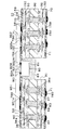
次に、本発明の第1実施形態に係る製造方法により製造されるプリント配線板10の構成について、図7、図8、図9、図10を参照して説明する。図7は、プリント配線板10の断面図を示している。図8は、図7に示すプリント配線板10にCPUチップ901、メモリチップ902を取り付けた半導体装置を示している。図9は、図7に示すプリント配線板10の平面図を示している。図10は、実装されるCPUチップ901、メモリチップ902の底面図を示す。
図9の平面図中に示すように、インターポーザ80のバンプ82A、82Bは、ピッチP2(約40μm)に配置されている。また、ビルドアップ多層配線板の半田バンプ78Sは、ピッチP1(約130μm)に配置されている。そして、耐熱基板80の信号線43のL/Sは、1/1μm〜3/3μmに設定されている。第1実施形態では、インターポーザ80はシリコンから成り、信号線83及びバンプ82B、バンプ82Aは、半導体製造工程を用いることでファインに製造されている。耐熱基板81を形成する材料としては、熱膨張係数2〜10ppmのシリコン、セラミック、ガラスを用いることができる。
(1)厚さ0.2〜0.8mmのガラスエポキシ樹脂またはBT(ビスマレイミドトリアジン)樹脂からなる絶縁性基板30の両面に5〜250μmの銅箔32がラミネートされている銅張積層板30Aを出発材料とした(図1(A))。まず、この銅張積層板をドリル削孔して通孔33を穿設し(図1(B))、無電解めっき処理および電解めっき処理を施し、スルーホール導体36を形成する(図1(C))。その後、スルーホール導体36を形成した基板30を水洗いし、乾燥した後、黒化処理、および、還元処理を行い、スルーホール36の側壁導体層及び表面に粗化面を形成する(図示せず)。
さらに、粗面化処理(粗化深さ3μm)した該基板の表面に、パラジウム触媒を付与することにより、層間樹脂絶縁層の表面およびバイアホール用開口の内壁面に触媒核を付着させた。
また、テーパ部を設けることで、充填樹脂とビルドアップ層(層間樹脂絶縁層)との接触面積が大きくなり、半導体素子との熱膨張係数の差により生じる応力を緩和できる。その結果、ビルドアップ層へ生じるクラックが抑制されると推測される。
第2実施形態のプリント配線板について、第2実施形態に係るプリント配線板の平面図を示す図11を参照して説明する。
第2実施形態のプリント配線板の構成は図7及び図9を参照して上述した第1実施形態と同様である。但し、第1実施形態では、貫通孔31の開口部が矩形になるように角柱形状に形成されたのに対して、第2実施形態では、貫通孔31の開口部が円形になるように円筒形状に形成されている。また、インターポーザ80は、角部が面取りされ、角部で応力が集中しないように構成されている。
11 多層プリント配線板
30 コア基板
36 スルーホール
40 樹脂充填層
50 層間樹脂絶縁層
58 導体回路
60 バイアホール
70 ソルダーレジスト層
78S 半田バンプ
80 耐熱基板
82A、82B バンプ
83 信号線
901 CPUチップ
902 メモリチップ
Claims (15)
- 第1面と第2面とを有する第1基板と、
当該第1基板を貫通する通孔の内部に形成されて表裏を電気的に接続するスルーホール導体と、
前記第1基板の第1面上に形成されていて、層間樹脂絶縁層と第1導体回路とが交互に積層されてなるビルドアップ層と、
を有し、
前記第1基板および前記ビルドアップ層には、前記第1基板を貫通する第1開口部と、前記ビルドアップ層を貫通し、当該ビルドアップ層の最外面に開口する第2開口部とを有する貫通孔が形成され、
前記第2開口部に収容されている第2基板と、
前記第2基板上に形成されている第2導体回路と、
前記第2開口部内に充填されている充填材と、
をさらに有する配線板であって、
前記第2開口部は、前記ビルドアップ層の最外面に向かいテーパするテーパ部を有する。 - 前記テーパ部はレーザーにより形成されている請求項1の配線板。
- 前記第1導体回路は、複数の半導体素子を実装する第1実装パッドを有する請求項1の配線板。
- 前記第2導体回路は、複数の半導体素子を実装する第2実装パッドを有する請求項1の配線板。
- 前記第2実装パッドのピッチは、前記第1実装パッドのピッチよりも小さい請求項1の配線板。
- 前記第2導体回路は、前記複数の半導体素子の間を接続する信号線である請求項1の配線板。
- 前記第2基板は、熱膨張係数2〜10ppmの材料から形成されている請求項1の配線板。
- 前記第2基板は、シリコン、セラミック、ガラスから選択されるいずれか1種からなる請求項1の配線板。
- 前記第2導体回路のL/Sは、前記第1導体回路のL/Sよりも小さい請求項1のプリント配線板。
- 前記第1導体回路は、電源用又はグランド用の導体である請求項1の配線板。
- 前記ビルドアップ層は受動素子を有する請求項1の配線板。
- 前記第2基板は受動素子を有する請求項1の配線板。
- 前記第2基板の角部は面取りされている請求項1の配線板。
- 第1面と第2面とを有する第1基板を準備することと、
当該第1基板の表裏を電気的に接続するスルーホール導体を前記第1基板を貫通する通孔の内部に形成することと、
前記第1基板の第1面上に、層間樹脂絶縁層と第1導体回路とが交互に積層されてなるビルドアップ層を形成することと、
前記第1基板および前記ビルドアップ層に、前記第1基板を貫通する第1開口部と、前記ビルドアップ層を貫通し、当該ビルドアップ層の最外面に開口する第2開口部とを有する貫通孔を形成することと、
前記第2開口部に、第2基板と該第2基板上に形成された第2導体回路とを有するインターポーザを収容することと、
前記第2開口部内に充填材を充填することと、
を含む配線板の製造方法であって、
前記第2開口部に、前記ビルドアップ層の最外面に向かいテーパするテーパ部を設ける。 - 前記テーパ部はレーザーにより形成されることを特徴とする請求項14の配線板の製造方法。
Applications Claiming Priority (4)
| Application Number | Priority Date | Filing Date | Title |
|---|---|---|---|
| US31902410P | 2010-03-30 | 2010-03-30 | |
| US61/319,024 | 2010-03-30 | ||
| US13/050,217 | 2011-03-17 | ||
| US13/050,217 US8654538B2 (en) | 2010-03-30 | 2011-03-17 | Wiring board and method for manufacturing the same |
Publications (2)
| Publication Number | Publication Date |
|---|---|
| JP2011211194A JP2011211194A (ja) | 2011-10-20 |
| JP5267604B2 true JP5267604B2 (ja) | 2013-08-21 |
Family
ID=44708299
Family Applications (1)
| Application Number | Title | Priority Date | Filing Date |
|---|---|---|---|
| JP2011062080A Active JP5267604B2 (ja) | 2010-03-30 | 2011-03-22 | 配線板及びその製造方法 |
Country Status (2)
| Country | Link |
|---|---|
| US (2) | US8654538B2 (ja) |
| JP (1) | JP5267604B2 (ja) |
Families Citing this family (77)
| Publication number | Priority date | Publication date | Assignee | Title |
|---|---|---|---|---|
| JP2013214578A (ja) * | 2012-03-30 | 2013-10-17 | Ibiden Co Ltd | 配線板及びその製造方法 |
| JP5931547B2 (ja) * | 2012-03-30 | 2016-06-08 | イビデン株式会社 | 配線板及びその製造方法 |
| US9406587B2 (en) | 2012-06-26 | 2016-08-02 | Intel Corporation | Substrate conductor structure and method |
| JP6157821B2 (ja) * | 2012-09-26 | 2017-07-05 | イビデン株式会社 | 配線板及びその製造方法 |
| JP2014082334A (ja) * | 2012-10-16 | 2014-05-08 | Ibiden Co Ltd | 配線板及びその製造方法 |
| JP6082233B2 (ja) * | 2012-10-31 | 2017-02-15 | イビデン株式会社 | 配線板及びその製造方法 |
| WO2014079478A1 (en) | 2012-11-20 | 2014-05-30 | Light In Light Srl | High speed laser processing of transparent materials |
| EP2754524B1 (de) | 2013-01-15 | 2015-11-25 | Corning Laser Technologies GmbH | Verfahren und Vorrichtung zum laserbasierten Bearbeiten von flächigen Substraten, d.h. Wafer oder Glaselement, unter Verwendung einer Laserstrahlbrennlinie |
| US8803310B1 (en) * | 2013-02-08 | 2014-08-12 | Unimicron Technology Corp. | Embedded electronic device package structure |
| EP2781296B1 (de) | 2013-03-21 | 2020-10-21 | Corning Laser Technologies GmbH | Vorrichtung und verfahren zum ausschneiden von konturen aus flächigen substraten mittels laser |
| JP2015050315A (ja) * | 2013-08-31 | 2015-03-16 | イビデン株式会社 | 結合型のプリント配線板及びその製造方法 |
| US9642259B2 (en) | 2013-10-30 | 2017-05-02 | Qualcomm Incorporated | Embedded bridge structure in a substrate |
| JP2015106615A (ja) * | 2013-11-29 | 2015-06-08 | イビデン株式会社 | プリント配線板、プリント配線板の製造方法 |
| US9815730B2 (en) | 2013-12-17 | 2017-11-14 | Corning Incorporated | Processing 3D shaped transparent brittle substrate |
| US10442719B2 (en) | 2013-12-17 | 2019-10-15 | Corning Incorporated | Edge chamfering methods |
| US10293436B2 (en) | 2013-12-17 | 2019-05-21 | Corning Incorporated | Method for rapid laser drilling of holes in glass and products made therefrom |
| US11556039B2 (en) | 2013-12-17 | 2023-01-17 | Corning Incorporated | Electrochromic coated glass articles and methods for laser processing the same |
| US9850160B2 (en) | 2013-12-17 | 2017-12-26 | Corning Incorporated | Laser cutting of display glass compositions |
| US9676167B2 (en) | 2013-12-17 | 2017-06-13 | Corning Incorporated | Laser processing of sapphire substrate and related applications |
| US9701563B2 (en) | 2013-12-17 | 2017-07-11 | Corning Incorporated | Laser cut composite glass article and method of cutting |
| US20150165560A1 (en) | 2013-12-17 | 2015-06-18 | Corning Incorporated | Laser processing of slots and holes |
| US11291146B2 (en) | 2014-03-07 | 2022-03-29 | Bridge Semiconductor Corp. | Leadframe substrate having modulator and crack inhibiting structure and flip chip assembly using the same |
| US10121768B2 (en) | 2015-05-27 | 2018-11-06 | Bridge Semiconductor Corporation | Thermally enhanced face-to-face semiconductor assembly with built-in heat spreader and method of making the same |
| US10354984B2 (en) | 2015-05-27 | 2019-07-16 | Bridge Semiconductor Corporation | Semiconductor assembly with electromagnetic shielding and thermally enhanced characteristics and method of making the same |
| TWI730945B (zh) | 2014-07-08 | 2021-06-21 | 美商康寧公司 | 用於雷射處理材料的方法與設備 |
| CN107073641B (zh) | 2014-07-14 | 2020-11-10 | 康宁股份有限公司 | 接口块;用于使用这种接口块切割在波长范围内透明的衬底的系统和方法 |
| WO2016010949A1 (en) | 2014-07-14 | 2016-01-21 | Corning Incorporated | Method and system for forming perforations |
| EP3169479B1 (en) | 2014-07-14 | 2019-10-02 | Corning Incorporated | Method of and system for arresting incident crack propagation in a transparent material |
| KR20170028943A (ko) * | 2014-07-14 | 2017-03-14 | 코닝 인코포레이티드 | 조정가능한 레이저 빔 촛점 라인을 사용하여 투명한 재료를 처리하는 방법 및 시스템 |
| JP2016029681A (ja) | 2014-07-25 | 2016-03-03 | イビデン株式会社 | 多層配線板及びその製造方法 |
| JP2016039214A (ja) | 2014-08-06 | 2016-03-22 | イビデン株式会社 | 電子部品内蔵用キャビティ付き配線板及びその製造方法 |
| JP6473595B2 (ja) * | 2014-10-10 | 2019-02-20 | イビデン株式会社 | 多層配線板及びその製造方法 |
| US10047001B2 (en) | 2014-12-04 | 2018-08-14 | Corning Incorporated | Glass cutting systems and methods using non-diffracting laser beams |
| CN107406293A (zh) | 2015-01-12 | 2017-11-28 | 康宁股份有限公司 | 使用多光子吸收方法来对经热回火的基板进行激光切割 |
| US11773004B2 (en) | 2015-03-24 | 2023-10-03 | Corning Incorporated | Laser cutting and processing of display glass compositions |
| KR20170131638A (ko) | 2015-03-27 | 2017-11-29 | 코닝 인코포레이티드 | 가스 투과성 유리창 및 이의 제작방법 |
| KR102163039B1 (ko) * | 2015-04-07 | 2020-10-08 | 삼성전기주식회사 | 인쇄회로기판, 그 제조방법, 및 전자부품 모듈 |
| JP6659247B2 (ja) * | 2015-06-16 | 2020-03-04 | デクセリアルズ株式会社 | 接続体、接続体の製造方法、検査方法 |
| KR102340053B1 (ko) * | 2015-06-18 | 2021-12-16 | 삼성전기주식회사 | 인쇄회로기판 및 인쇄회로기판의 제조 방법 |
| US9706662B2 (en) * | 2015-06-30 | 2017-07-11 | Raytheon Company | Adaptive interposer and electronic apparatus |
| WO2017011296A1 (en) | 2015-07-10 | 2017-01-19 | Corning Incorporated | Methods of continuous fabrication of holes in flexible substrate sheets and products relating to the same |
| US10096573B2 (en) * | 2015-07-28 | 2018-10-09 | Bridge Semiconductor Corporation | Face-to-face semiconductor assembly having semiconductor device in dielectric recess |
| JP2017050313A (ja) * | 2015-08-31 | 2017-03-09 | イビデン株式会社 | プリント配線板及びプリント配線板の製造方法 |
| JP2017050315A (ja) * | 2015-08-31 | 2017-03-09 | イビデン株式会社 | プリント配線板及びプリント配線板の製造方法 |
| EP3416188A4 (en) * | 2016-02-10 | 2019-10-16 | Renesas Electronics Corporation | SEMICONDUCTOR COMPONENT |
| JP6938543B2 (ja) | 2016-05-06 | 2021-09-22 | コーニング インコーポレイテッド | 透明基板からの、輪郭設定された形状のレーザ切断及び取り外し |
| JP2017202939A (ja) * | 2016-05-09 | 2017-11-16 | 旭硝子株式会社 | ガラス基板の製造方法およびガラス板 |
| US10410883B2 (en) | 2016-06-01 | 2019-09-10 | Corning Incorporated | Articles and methods of forming vias in substrates |
| US10794679B2 (en) | 2016-06-29 | 2020-10-06 | Corning Incorporated | Method and system for measuring geometric parameters of through holes |
| KR20190035805A (ko) | 2016-07-29 | 2019-04-03 | 코닝 인코포레이티드 | 레이저 처리를 위한 장치 및 방법 |
| KR102632563B1 (ko) | 2016-08-05 | 2024-02-02 | 삼성전자주식회사 | 반도체 패키지 |
| KR102423775B1 (ko) | 2016-08-30 | 2022-07-22 | 코닝 인코포레이티드 | 투명 재료의 레이저 가공 |
| US10730783B2 (en) | 2016-09-30 | 2020-08-04 | Corning Incorporated | Apparatuses and methods for laser processing transparent workpieces using non-axisymmetric beam spots |
| KR102428350B1 (ko) | 2016-10-24 | 2022-08-02 | 코닝 인코포레이티드 | 시트형 유리 기판의 레이저 기반 기계 가공을 위한 기판 프로세싱 스테이션 |
| US10752534B2 (en) | 2016-11-01 | 2020-08-25 | Corning Incorporated | Apparatuses and methods for laser processing laminate workpiece stacks |
| US10688599B2 (en) | 2017-02-09 | 2020-06-23 | Corning Incorporated | Apparatus and methods for laser processing transparent workpieces using phase shifted focal lines |
| WO2018182597A1 (en) * | 2017-03-29 | 2018-10-04 | Intel Corporation | Microelectronic device with embedded die substrate on interposer |
| CN107068845B (zh) * | 2017-05-19 | 2024-03-19 | 深圳大道半导体有限公司 | 组合式半导体结构及灯具 |
| US11078112B2 (en) | 2017-05-25 | 2021-08-03 | Corning Incorporated | Silica-containing substrates with vias having an axially variable sidewall taper and methods for forming the same |
| US10580725B2 (en) | 2017-05-25 | 2020-03-03 | Corning Incorporated | Articles having vias with geometry attributes and methods for fabricating the same |
| US10687419B2 (en) | 2017-06-13 | 2020-06-16 | Advanced Semiconductor Engineering, Inc. | Semiconductor package device and method of manufacturing the same |
| US10626040B2 (en) | 2017-06-15 | 2020-04-21 | Corning Incorporated | Articles capable of individual singulation |
| TWI736780B (zh) | 2017-10-31 | 2021-08-21 | 台灣積體電路製造股份有限公司 | 晶片封裝及其形成方法 |
| US11322449B2 (en) * | 2017-10-31 | 2022-05-03 | Taiwan Semiconductor Manufacturing Co., Ltd. | Package with fan-out structures |
| US12180108B2 (en) | 2017-12-19 | 2024-12-31 | Corning Incorporated | Methods for etching vias in glass-based articles employing positive charge organic molecules |
| US11554984B2 (en) | 2018-02-22 | 2023-01-17 | Corning Incorporated | Alkali-free borosilicate glasses with low post-HF etch roughness |
| US11322444B2 (en) | 2018-03-23 | 2022-05-03 | Intel Corporation | Lithographic cavity formation to enable EMIB bump pitch scaling |
| JP7295373B2 (ja) * | 2018-09-28 | 2023-06-21 | 日亜化学工業株式会社 | プリント回路板及びその製造方法 |
| US11600567B2 (en) * | 2019-07-31 | 2023-03-07 | Advanced Semiconductor Engineering, Inc. | Semiconductor device package and method for manufacturing the same |
| CN113545170A (zh) * | 2019-10-31 | 2021-10-22 | 鹏鼎控股(深圳)股份有限公司 | 薄型电路板及其制造方法 |
| US11094637B2 (en) * | 2019-11-06 | 2021-08-17 | International Business Machines Corporation | Multi-chip package structures having embedded chip interconnect bridges and fan-out redistribution layers |
| KR102643424B1 (ko) | 2019-12-13 | 2024-03-06 | 삼성전자주식회사 | 반도체 패키지 |
| US11527462B2 (en) * | 2019-12-13 | 2022-12-13 | International Business Machines Corporation | Circuit substrate with mixed pitch wiring |
| US12355000B2 (en) * | 2020-11-10 | 2025-07-08 | Qualcomm Incorporated | Package comprising a substrate and a high-density interconnect integrated device |
| CN112689381A (zh) * | 2021-02-04 | 2021-04-20 | 深圳市同创鑫电子有限公司 | 一种印刷电路板和印刷电路板的制造方法 |
| US12469811B2 (en) | 2021-03-26 | 2025-11-11 | Qualcomm Incorporated | Package comprising wire bonds coupled to integrated devices |
| US20240249988A1 (en) * | 2023-01-19 | 2024-07-25 | Advanced Semiconductor Engineering, Inc. | Semiconductor device package and method of manufacturing the same |
Family Cites Families (21)
| Publication number | Priority date | Publication date | Assignee | Title |
|---|---|---|---|---|
| US4528530A (en) * | 1982-09-24 | 1985-07-09 | International Business Machines Corporation | Low temperature electronic package having a superconductive interposer for interconnecting strip type circuits |
| US5831810A (en) * | 1996-08-21 | 1998-11-03 | International Business Machines Corporation | Electronic component package with decoupling capacitors completely within die receiving cavity of substrate |
| TW449844B (en) * | 1997-05-17 | 2001-08-11 | Hyundai Electronics Ind | Ball grid array package having an integrated circuit chip |
| DE69934981T2 (de) | 1998-05-19 | 2007-11-15 | Ibiden Co., Ltd., Ogaki | Gedruckte leiterplatte und verfahren zur herstellung |
| US6153829A (en) * | 1998-09-15 | 2000-11-28 | Intel Corporation | Split cavity wall plating for an integrated circuit package |
| JP3792445B2 (ja) * | 1999-03-30 | 2006-07-05 | 日本特殊陶業株式会社 | コンデンサ付属配線基板 |
| JP3860380B2 (ja) | 1999-04-06 | 2006-12-20 | 富士通株式会社 | 配線基板及びこれを使用したチップモジュール |
| JP3659167B2 (ja) | 1999-04-16 | 2005-06-15 | 松下電器産業株式会社 | モジュール部品とその製造方法 |
| US6366468B1 (en) * | 2000-04-28 | 2002-04-02 | Hewlett-Packard Company | Self-aligned common carrier |
| US7247932B1 (en) * | 2000-05-19 | 2007-07-24 | Megica Corporation | Chip package with capacitor |
| US6713860B2 (en) * | 2002-02-01 | 2004-03-30 | Intel Corporation | Electronic assembly and system with vertically connected capacitors |
| US20030183934A1 (en) * | 2002-03-29 | 2003-10-02 | Barrett Joseph C. | Method and apparatus for stacking multiple die in a flip chip semiconductor package |
| JP2003298234A (ja) | 2002-04-01 | 2003-10-17 | Hitachi Cable Ltd | 多層配線板及びその製造方法、ならびに配線基板 |
| TW550721B (en) * | 2002-04-18 | 2003-09-01 | United Test Ct Inc | Test fixture for semiconductor package |
| JP2003324183A (ja) * | 2002-05-07 | 2003-11-14 | Mitsubishi Electric Corp | 半導体装置 |
| JP2004288834A (ja) * | 2003-03-20 | 2004-10-14 | Fujitsu Ltd | 電子部品の実装方法、実装構造及びパッケージ基板 |
| EP1860694A1 (en) * | 2005-03-16 | 2007-11-28 | Yamaha Corporation | Semiconductor device, semiconductor device manufacturing method and cover frame |
| JP4581768B2 (ja) * | 2005-03-16 | 2010-11-17 | ソニー株式会社 | 半導体装置の製造方法 |
| US7932471B2 (en) * | 2005-08-05 | 2011-04-26 | Ngk Spark Plug Co., Ltd. | Capacitor for incorporation in wiring board, wiring board, method of manufacturing wiring board, and ceramic chip for embedment |
| JP5101240B2 (ja) | 2007-10-25 | 2012-12-19 | 日本特殊陶業株式会社 | 板状部品内蔵配線基板 |
| JP5112005B2 (ja) | 2007-10-25 | 2013-01-09 | 日本特殊陶業株式会社 | 板状部品内蔵配線基板及びその製造方法 |
-
2011
- 2011-03-17 US US13/050,217 patent/US8654538B2/en active Active
- 2011-03-22 JP JP2011062080A patent/JP5267604B2/ja active Active
-
2014
- 2014-01-22 US US14/160,766 patent/US8971053B2/en active Active
Also Published As
| Publication number | Publication date |
|---|---|
| US20140133119A1 (en) | 2014-05-15 |
| US20110240357A1 (en) | 2011-10-06 |
| US8654538B2 (en) | 2014-02-18 |
| JP2011211194A (ja) | 2011-10-20 |
| US8971053B2 (en) | 2015-03-03 |
Similar Documents
| Publication | Publication Date | Title |
|---|---|---|
| JP5267604B2 (ja) | 配線板及びその製造方法 | |
| US7923367B2 (en) | Multilayer wiring substrate mounted with electronic component and method for manufacturing the same | |
| JP3849573B2 (ja) | 電子装置 | |
| US20070096292A1 (en) | Electronic-part built-in substrate and manufacturing method therefor | |
| JPH11233678A (ja) | Icパッケージの製造方法 | |
| JP2002016173A (ja) | 半導体装置 | |
| JPWO2007126090A1 (ja) | 回路基板、電子デバイス装置及び回路基板の製造方法 | |
| JP2015106615A (ja) | プリント配線板、プリント配線板の製造方法 | |
| JP5048005B2 (ja) | 金属バンプを持つプリント基板及びその製造方法 | |
| CN102132639A (zh) | 电子部件内置线路板及其制造方法 | |
| CN101683006A (zh) | 电子部件内置线路板及其制造方法 | |
| JP2001015650A (ja) | ボールグリッドアレイパッケージとその製造方法 | |
| KR20150064976A (ko) | 인쇄회로기판 및 그 제조방법 | |
| KR20140143567A (ko) | 반도체 패키지 기판 및 반도체 패키지 기판 제조 방법 | |
| JP5530859B2 (ja) | 配線基板の製造方法 | |
| JP2013110329A (ja) | コンデンサモジュール内蔵配線基板 | |
| US8546922B2 (en) | Wiring board | |
| JP7211757B2 (ja) | 配線基板 | |
| TWI778056B (zh) | 佈線基板和製造佈線基板的方法 | |
| JP4196606B2 (ja) | 配線板の製造方法 | |
| KR101969647B1 (ko) | 포스트를 구비한 회로기판 제조방법 | |
| JP2019186256A (ja) | プリント配線板およびその製造方法 | |
| JP2013122963A (ja) | 配線基板 | |
| JP5516619B2 (ja) | 電子部品の製造方法 | |
| JP2001015912A (ja) | 多層プリント配線板及び多層プリント配線板の製造方法 |
Legal Events
| Date | Code | Title | Description |
|---|---|---|---|
| A131 | Notification of reasons for refusal |
Free format text: JAPANESE INTERMEDIATE CODE: A131 Effective date: 20120904 |
|
| A521 | Request for written amendment filed |
Free format text: JAPANESE INTERMEDIATE CODE: A523 Effective date: 20121031 |
|
| TRDD | Decision of grant or rejection written | ||
| A01 | Written decision to grant a patent or to grant a registration (utility model) |
Free format text: JAPANESE INTERMEDIATE CODE: A01 Effective date: 20130409 |
|
| A61 | First payment of annual fees (during grant procedure) |
Free format text: JAPANESE INTERMEDIATE CODE: A61 Effective date: 20130422 |
|
| R150 | Certificate of patent or registration of utility model |
Ref document number: 5267604 Country of ref document: JP Free format text: JAPANESE INTERMEDIATE CODE: R150 Free format text: JAPANESE INTERMEDIATE CODE: R150 |
|
| R250 | Receipt of annual fees |
Free format text: JAPANESE INTERMEDIATE CODE: R250 |
|
| R250 | Receipt of annual fees |
Free format text: JAPANESE INTERMEDIATE CODE: R250 |
|
| R250 | Receipt of annual fees |
Free format text: JAPANESE INTERMEDIATE CODE: R250 |
|
| R250 | Receipt of annual fees |
Free format text: JAPANESE INTERMEDIATE CODE: R250 |
|
| R250 | Receipt of annual fees |
Free format text: JAPANESE INTERMEDIATE CODE: R250 |
|
| R250 | Receipt of annual fees |
Free format text: JAPANESE INTERMEDIATE CODE: R250 |
|
| R250 | Receipt of annual fees |
Free format text: JAPANESE INTERMEDIATE CODE: R250 |
|
| R250 | Receipt of annual fees |
Free format text: JAPANESE INTERMEDIATE CODE: R250 |
|
| R250 | Receipt of annual fees |
Free format text: JAPANESE INTERMEDIATE CODE: R250 |
|
| R250 | Receipt of annual fees |
Free format text: JAPANESE INTERMEDIATE CODE: R250 |
|
| R250 | Receipt of annual fees |
Free format text: JAPANESE INTERMEDIATE CODE: R250 |