JP6132014B2 - 半導体装置および半導体装置の製造方法 - Google Patents
半導体装置および半導体装置の製造方法 Download PDFInfo
- Publication number
- JP6132014B2 JP6132014B2 JP2015513808A JP2015513808A JP6132014B2 JP 6132014 B2 JP6132014 B2 JP 6132014B2 JP 2015513808 A JP2015513808 A JP 2015513808A JP 2015513808 A JP2015513808 A JP 2015513808A JP 6132014 B2 JP6132014 B2 JP 6132014B2
- Authority
- JP
- Japan
- Prior art keywords
- wire
- semiconductor device
- bonding
- electrode
- metal film
- Prior art date
- Legal status (The legal status is an assumption and is not a legal conclusion. Google has not performed a legal analysis and makes no representation as to the accuracy of the status listed.)
- Active
Links
Images


Classifications
-
- H—ELECTRICITY
- H10—SEMICONDUCTOR DEVICES; ELECTRIC SOLID-STATE DEVICES NOT OTHERWISE PROVIDED FOR
- H10W—GENERIC PACKAGES, INTERCONNECTIONS, CONNECTORS OR OTHER CONSTRUCTIONAL DETAILS OF DEVICES COVERED BY CLASS H10
- H10W72/00—Interconnections or connectors in packages
- H10W72/01—Manufacture or treatment
- H10W72/019—Manufacture or treatment of bond pads
-
- H—ELECTRICITY
- H10—SEMICONDUCTOR DEVICES; ELECTRIC SOLID-STATE DEVICES NOT OTHERWISE PROVIDED FOR
- H10W—GENERIC PACKAGES, INTERCONNECTIONS, CONNECTORS OR OTHER CONSTRUCTIONAL DETAILS OF DEVICES COVERED BY CLASS H10
- H10W72/00—Interconnections or connectors in packages
- H10W72/01—Manufacture or treatment
- H10W72/015—Manufacture or treatment of bond wires
-
- H—ELECTRICITY
- H10—SEMICONDUCTOR DEVICES; ELECTRIC SOLID-STATE DEVICES NOT OTHERWISE PROVIDED FOR
- H10W—GENERIC PACKAGES, INTERCONNECTIONS, CONNECTORS OR OTHER CONSTRUCTIONAL DETAILS OF DEVICES COVERED BY CLASS H10
- H10W72/00—Interconnections or connectors in packages
- H10W72/071—Connecting or disconnecting
- H10W72/075—Connecting or disconnecting of bond wires
- H10W72/07531—Techniques
- H10W72/07532—Compression bonding, e.g. thermocompression bonding
- H10W72/07533—Ultrasonic bonding, e.g. thermosonic bonding
-
- H—ELECTRICITY
- H10—SEMICONDUCTOR DEVICES; ELECTRIC SOLID-STATE DEVICES NOT OTHERWISE PROVIDED FOR
- H10W—GENERIC PACKAGES, INTERCONNECTIONS, CONNECTORS OR OTHER CONSTRUCTIONAL DETAILS OF DEVICES COVERED BY CLASS H10
- H10W72/00—Interconnections or connectors in packages
- H10W72/071—Connecting or disconnecting
- H10W72/075—Connecting or disconnecting of bond wires
- H10W72/07551—Connecting or disconnecting of bond wires characterised by changes in properties of the bond wires during the connecting
- H10W72/07555—Connecting or disconnecting of bond wires characterised by changes in properties of the bond wires during the connecting changes in materials
-
- H—ELECTRICITY
- H10—SEMICONDUCTOR DEVICES; ELECTRIC SOLID-STATE DEVICES NOT OTHERWISE PROVIDED FOR
- H10W—GENERIC PACKAGES, INTERCONNECTIONS, CONNECTORS OR OTHER CONSTRUCTIONAL DETAILS OF DEVICES COVERED BY CLASS H10
- H10W72/00—Interconnections or connectors in packages
- H10W72/30—Die-attach connectors
- H10W72/351—Materials of die-attach connectors
- H10W72/352—Materials of die-attach connectors comprising metals or metalloids, e.g. solders
-
- H—ELECTRICITY
- H10—SEMICONDUCTOR DEVICES; ELECTRIC SOLID-STATE DEVICES NOT OTHERWISE PROVIDED FOR
- H10W—GENERIC PACKAGES, INTERCONNECTIONS, CONNECTORS OR OTHER CONSTRUCTIONAL DETAILS OF DEVICES COVERED BY CLASS H10
- H10W72/00—Interconnections or connectors in packages
- H10W72/50—Bond wires
- H10W72/551—Materials of bond wires
- H10W72/552—Materials of bond wires comprising metals or metalloids, e.g. silver
- H10W72/5524—Materials of bond wires comprising metals or metalloids, e.g. silver comprising aluminium [Al]
-
- H—ELECTRICITY
- H10—SEMICONDUCTOR DEVICES; ELECTRIC SOLID-STATE DEVICES NOT OTHERWISE PROVIDED FOR
- H10W—GENERIC PACKAGES, INTERCONNECTIONS, CONNECTORS OR OTHER CONSTRUCTIONAL DETAILS OF DEVICES COVERED BY CLASS H10
- H10W72/00—Interconnections or connectors in packages
- H10W72/50—Bond wires
- H10W72/551—Materials of bond wires
- H10W72/552—Materials of bond wires comprising metals or metalloids, e.g. silver
- H10W72/5525—Materials of bond wires comprising metals or metalloids, e.g. silver comprising copper [Cu]
-
- H—ELECTRICITY
- H10—SEMICONDUCTOR DEVICES; ELECTRIC SOLID-STATE DEVICES NOT OTHERWISE PROVIDED FOR
- H10W—GENERIC PACKAGES, INTERCONNECTIONS, CONNECTORS OR OTHER CONSTRUCTIONAL DETAILS OF DEVICES COVERED BY CLASS H10
- H10W72/00—Interconnections or connectors in packages
- H10W72/50—Bond wires
- H10W72/59—Bond pads specially adapted therefor
-
- H—ELECTRICITY
- H10—SEMICONDUCTOR DEVICES; ELECTRIC SOLID-STATE DEVICES NOT OTHERWISE PROVIDED FOR
- H10W—GENERIC PACKAGES, INTERCONNECTIONS, CONNECTORS OR OTHER CONSTRUCTIONAL DETAILS OF DEVICES COVERED BY CLASS H10
- H10W72/00—Interconnections or connectors in packages
- H10W72/851—Dispositions of multiple connectors or interconnections
- H10W72/874—On different surfaces
- H10W72/884—Die-attach connectors and bond wires
-
- H—ELECTRICITY
- H10—SEMICONDUCTOR DEVICES; ELECTRIC SOLID-STATE DEVICES NOT OTHERWISE PROVIDED FOR
- H10W—GENERIC PACKAGES, INTERCONNECTIONS, CONNECTORS OR OTHER CONSTRUCTIONAL DETAILS OF DEVICES COVERED BY CLASS H10
- H10W72/00—Interconnections or connectors in packages
- H10W72/90—Bond pads, in general
- H10W72/921—Structures or relative sizes of bond pads
- H10W72/923—Bond pads having multiple stacked layers
-
- H—ELECTRICITY
- H10—SEMICONDUCTOR DEVICES; ELECTRIC SOLID-STATE DEVICES NOT OTHERWISE PROVIDED FOR
- H10W—GENERIC PACKAGES, INTERCONNECTIONS, CONNECTORS OR OTHER CONSTRUCTIONAL DETAILS OF DEVICES COVERED BY CLASS H10
- H10W72/00—Interconnections or connectors in packages
- H10W72/90—Bond pads, in general
- H10W72/951—Materials of bond pads
- H10W72/952—Materials of bond pads comprising metals or metalloids, e.g. PbSn, Ag or Cu
-
- H—ELECTRICITY
- H10—SEMICONDUCTOR DEVICES; ELECTRIC SOLID-STATE DEVICES NOT OTHERWISE PROVIDED FOR
- H10W—GENERIC PACKAGES, INTERCONNECTIONS, CONNECTORS OR OTHER CONSTRUCTIONAL DETAILS OF DEVICES COVERED BY CLASS H10
- H10W90/00—Package configurations
- H10W90/701—Package configurations characterised by the relative positions of pads or connectors relative to package parts
- H10W90/731—Package configurations characterised by the relative positions of pads or connectors relative to package parts of die-attach connectors
- H10W90/734—Package configurations characterised by the relative positions of pads or connectors relative to package parts of die-attach connectors between a chip and a stacked insulating package substrate, interposer or RDL
-
- H—ELECTRICITY
- H10—SEMICONDUCTOR DEVICES; ELECTRIC SOLID-STATE DEVICES NOT OTHERWISE PROVIDED FOR
- H10W—GENERIC PACKAGES, INTERCONNECTIONS, CONNECTORS OR OTHER CONSTRUCTIONAL DETAILS OF DEVICES COVERED BY CLASS H10
- H10W90/00—Package configurations
- H10W90/701—Package configurations characterised by the relative positions of pads or connectors relative to package parts
- H10W90/751—Package configurations characterised by the relative positions of pads or connectors relative to package parts of bond wires
- H10W90/754—Package configurations characterised by the relative positions of pads or connectors relative to package parts of bond wires between a chip and a stacked insulating package substrate, interposer or RDL
Landscapes
- Wire Bonding (AREA)
- Engineering & Computer Science (AREA)
- Manufacturing & Machinery (AREA)
Description
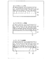
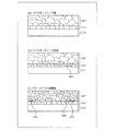
実施の形態にかかる半導体装置の構造について説明する。図1は、実施の形態にかかる半導体装置の構造を示す断面図である。図2は、図1の半導体素子の構造を模式的に示す断面図である。図1,2に示すように、実施の形態にかかる半導体装置は、半導体素子(半導体チップ)1と、セラミクス絶縁基板(DCB基板)などの絶縁基板2と、銅(Cu)ベース6と、ワイヤ7とを備えたモジュール構造の半導体装置である。絶縁基板2は、絶縁層3のおもて面側に例えばCuなどからなる回路層4が設けられ、裏面側に裏銅箔5が設けられている。
1a はんだ接合層
2 絶縁基板
3 絶縁層
4 回路層
5 裏銅箔
6 Cuベース
7 ワイヤ
11 半導体基板
12 おもて面電極
13 裏面電極
14 おもて面金属膜
20 ワイヤの接合界面
21 クラック
Claims (14)
- ワイヤボンディングによって半導体素子の電極とワイヤとを電気的に接続してなる半導体装置において、
前記電極の表面に、前記ワイヤよりも硬度が高い金属膜が設けられており、
前記ワイヤは、ワイヤボンディングによって前記金属膜に接合されており、
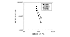
前記ワイヤの前記金属膜との接合界面の再結晶温度が175℃以上であり、
前記ワイヤの前記接合界面には、粒径が15μm以下の結晶粒のみを含み、
前記ワイヤの前記接合界面から離れた部分は、粒径が15μmより大きい結晶粒を含み、
前記半導体素子の接合温度は前記再結晶温度未満であることを特徴とする半導体装置。 - 前記ワイヤは、鉄を0.2質量%以上2.0質量%以下含み、および残部が純度99.99%以上のアルミニウムからなることを特徴とする請求項1に記載の半導体装置。
- 前記ワイヤの線径は、100μm以上であることを特徴とする請求項1または2に記載の半導体装置。
- 前記ワイヤの線径は、500μm以下であることを特徴とする請求項3に記載の半導体装置。
- 前記ワイヤの硬度は、前記電極の硬度よりも高いことを特徴とする請求項1〜4のいずれか一つに記載の半導体装置。
- 前記金属膜はニッケルめっき膜であることを特徴とする請求項1〜5のいずれか一つに記載の半導体装置。
- 前記ニッケルめっき膜の膜厚は3μm〜7μmであることを特徴とする請求項6に記載の半導体装置。
- 前記金属膜は銅めっき膜であることを特徴とする請求項1〜5のいずれか一つに記載の半導体装置。
- 前記銅めっき膜の膜厚は4.5μm〜10.5μmであることを特徴とする請求項8に記載の半導体装置。
- 半導体素子の電極とワイヤとを電気的に接続する半導体装置の製造方法において、
前記ワイヤよりも硬度が高い金属膜を前記電極の表面に設ける第1工程と、
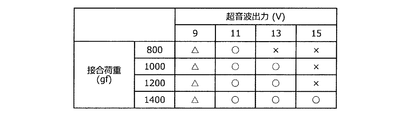
ワイヤボンディング時に当該ワイヤボンディングの超音波振動により前記ワイヤの前記金属膜との接合界面の結晶粒を15μm以下の粒径の結晶粒のみにして前記ワイヤを前記金属膜に接合する第2工程と、
を含み、
前記第2工程では、前記ワイヤの前記接合界面から離れた部分の粒径を15μmより大きい結晶粒を含んだままの状態で維持し、
前記第2工程よりも後に行う工程では、前記半導体素子にかかる熱履歴の温度が、前記ワイヤの前記接合界面の再結晶温度未満であることを特徴とする半導体装置の製造方法。 - 接合温度が前記再結晶温度未満の前記半導体素子を用いることを特徴とする請求項10に記載の半導体装置の製造方法。
- 前記ワイヤは、鉄を0.2質量%以上2.0質量%以下含み、および残部が純度99.99%以上のアルミニウムからなることを特徴とする請求項10または11に記載の半導体装置の製造方法。
- 前記ワイヤの線径は、100μm以上であることを特徴とする請求項10〜12のいずれか一つに記載の半導体装置の製造方法。
- 前記ワイヤの線径は、500μm以下であることを特徴とする請求項13に記載の半導体装置の製造方法。
Applications Claiming Priority (3)
| Application Number | Priority Date | Filing Date | Title |
|---|---|---|---|
| JP2013092110 | 2013-04-25 | ||
| JP2013092110 | 2013-04-25 | ||
| PCT/JP2014/061457 WO2014175343A1 (ja) | 2013-04-25 | 2014-04-23 | 半導体装置および半導体装置の製造方法 |
Publications (2)
| Publication Number | Publication Date |
|---|---|
| JPWO2014175343A1 JPWO2014175343A1 (ja) | 2017-02-23 |
| JP6132014B2 true JP6132014B2 (ja) | 2017-05-24 |
Family
ID=51791911
Family Applications (1)
| Application Number | Title | Priority Date | Filing Date |
|---|---|---|---|
| JP2015513808A Active JP6132014B2 (ja) | 2013-04-25 | 2014-04-23 | 半導体装置および半導体装置の製造方法 |
Country Status (5)
| Country | Link |
|---|---|
| US (1) | US9748186B2 (ja) |
| JP (1) | JP6132014B2 (ja) |
| CN (1) | CN105190858B (ja) |
| DE (1) | DE112014002135T5 (ja) |
| WO (1) | WO2014175343A1 (ja) |
Families Citing this family (23)
| Publication number | Priority date | Publication date | Assignee | Title |
|---|---|---|---|---|
| DE112016001142B4 (de) * | 2015-03-10 | 2020-01-16 | Mitsubishi Electric Corporation | Leistungs-Halbleitervorrichtung |
| US10886250B2 (en) | 2015-07-10 | 2021-01-05 | Invensas Corporation | Structures and methods for low temperature bonding using nanoparticles |
| JP6665664B2 (ja) * | 2016-04-27 | 2020-03-13 | 富士電機株式会社 | 半導体装置及びその製造方法 |
| TWI822659B (zh) | 2016-10-27 | 2023-11-21 | 美商艾德亞半導體科技有限責任公司 | 用於低溫接合的結構和方法 |
| US10515913B2 (en) | 2017-03-17 | 2019-12-24 | Invensas Bonding Technologies, Inc. | Multi-metal contact structure |
| US10446441B2 (en) | 2017-06-05 | 2019-10-15 | Invensas Corporation | Flat metal features for microelectronics applications |
| CN111344840B (zh) * | 2017-11-22 | 2023-07-07 | 三菱电机株式会社 | 半导体装置以及半导体装置的制造方法 |
| JP6698231B2 (ja) * | 2018-02-01 | 2020-05-27 | パナソニック株式会社 | 半導体装置および半導体装置の製造方法 |
| EP3550596B1 (en) * | 2018-04-04 | 2024-09-04 | Infineon Technologies AG | Arrangements and method for providing a wire bond connection |
| US10790262B2 (en) | 2018-04-11 | 2020-09-29 | Invensas Bonding Technologies, Inc. | Low temperature bonded structures |
| US11244916B2 (en) | 2018-04-11 | 2022-02-08 | Invensas Bonding Technologies, Inc. | Low temperature bonded structures |
| US11244920B2 (en) | 2018-12-18 | 2022-02-08 | Invensas Bonding Technologies, Inc. | Method and structures for low temperature device bonding |
| CN110158020B (zh) * | 2019-04-09 | 2020-04-21 | 山东大学 | 一种超声辅助感应加热制备纳米结构氧化膜的方法 |
| WO2021014007A1 (en) * | 2019-07-25 | 2021-01-28 | Abb Power Grids Switzerland Ag | Power semiconductor module |
| US11735523B2 (en) | 2020-05-19 | 2023-08-22 | Adeia Semiconductor Bonding Technologies Inc. | Laterally unconfined structure |
| CN112201628A (zh) * | 2020-08-24 | 2021-01-08 | 株洲中车时代半导体有限公司 | 一种功率模块封装结构及其制备方法 |
| CN116848631A (zh) * | 2020-12-30 | 2023-10-03 | 美商艾德亚半导体接合科技有限公司 | 具有导电特征的结构及其形成方法 |
| WO2022163695A1 (ja) * | 2021-01-28 | 2022-08-04 | 三菱電機株式会社 | 半導体装置、電力変換装置および半導体装置の製造方法 |
| JP7619723B2 (ja) * | 2021-08-30 | 2025-01-22 | ミネベアパワーデバイス株式会社 | 半導体装置及びその製造方法 |
| US12512425B2 (en) | 2022-04-25 | 2025-12-30 | Adeia Semiconductor Bonding Technologies Inc. | Expansion controlled structure for direct bonding and method of forming same |
| WO2024029286A1 (ja) * | 2022-08-03 | 2024-02-08 | ローム株式会社 | 半導体装置、および、半導体装置の製造方法 |
| US12545010B2 (en) | 2022-12-29 | 2026-02-10 | Adeia Semiconductor Bonding Technologies Inc. | Directly bonded metal structures having oxide layers therein |
| US12506114B2 (en) | 2022-12-29 | 2025-12-23 | Adeia Semiconductor Bonding Technologies Inc. | Directly bonded metal structures having aluminum features and methods of preparing same |
Family Cites Families (13)
| Publication number | Priority date | Publication date | Assignee | Title |
|---|---|---|---|---|
| JPS61163235A (ja) | 1985-01-09 | 1986-07-23 | Toshiba Corp | 半導体素子用ボンデイング線 |
| JPS63148646A (ja) * | 1986-12-12 | 1988-06-21 | Toshiba Corp | 半導体装置 |
| JPH07135234A (ja) | 1993-11-09 | 1995-05-23 | Hitachi Ltd | パワー半導体モジュール |
| JPH088288A (ja) | 1994-06-20 | 1996-01-12 | Hitachi Ltd | 半導体装置 |
| JPH08330710A (ja) * | 1995-06-05 | 1996-12-13 | Nippon Paint Co Ltd | プリント配線板電極部の金属めっき加工方法 |
| JP2004200644A (ja) * | 2002-10-22 | 2004-07-15 | Kyocera Corp | 配線基板 |
| JP3918724B2 (ja) * | 2002-11-28 | 2007-05-23 | トヨタ自動車株式会社 | ワイヤが接合されている半導体装置の製造方法 |
| JP4696532B2 (ja) * | 2004-05-20 | 2011-06-08 | 株式会社デンソー | パワー複合集積型半導体装置およびその製造方法 |
| JP2008311383A (ja) | 2007-06-14 | 2008-12-25 | Ibaraki Univ | ボンディングワイヤ、それを使用したボンディング方法及び半導体装置並びに接続部構造 |
| JP5214936B2 (ja) * | 2007-09-21 | 2013-06-19 | 富士電機株式会社 | 半導体装置 |
| JP2010251483A (ja) * | 2009-04-14 | 2010-11-04 | Renesas Electronics Corp | 半導体装置およびその製造方法 |
| CN102244062B (zh) * | 2011-07-26 | 2015-04-22 | 日月光半导体制造股份有限公司 | 半导体封装结构以及半导体封装工艺 |
| JP5159000B1 (ja) * | 2012-06-13 | 2013-03-06 | 田中電子工業株式会社 | 半導体装置接続用アルミニウム合金細線 |
-
2014
- 2014-04-23 JP JP2015513808A patent/JP6132014B2/ja active Active
- 2014-04-23 DE DE112014002135.0T patent/DE112014002135T5/de active Pending
- 2014-04-23 CN CN201480012154.0A patent/CN105190858B/zh active Active
- 2014-04-23 WO PCT/JP2014/061457 patent/WO2014175343A1/ja not_active Ceased
-
2015
- 2015-09-03 US US14/845,256 patent/US9748186B2/en active Active
Also Published As
| Publication number | Publication date |
|---|---|
| JPWO2014175343A1 (ja) | 2017-02-23 |
| DE112014002135T5 (de) | 2016-01-14 |
| CN105190858B (zh) | 2018-11-06 |
| US9748186B2 (en) | 2017-08-29 |
| WO2014175343A1 (ja) | 2014-10-30 |
| US20150380368A1 (en) | 2015-12-31 |
| CN105190858A (zh) | 2015-12-23 |
Similar Documents
| Publication | Publication Date | Title |
|---|---|---|
| JP6132014B2 (ja) | 半導体装置および半導体装置の製造方法 | |
| JP6895131B2 (ja) | 半導体装置用はんだ材 | |
| JP5159001B1 (ja) | アルミニウム合金ボンディングワイヤ | |
| JP5214936B2 (ja) | 半導体装置 | |
| JP3988735B2 (ja) | 半導体装置及びその製造方法 | |
| JP6056968B2 (ja) | 半導体装置 | |
| JPWO2017217145A1 (ja) | はんだ接合部 | |
| CN109075159B (zh) | 半导体装置及其制造方法 | |
| WO2012049893A1 (ja) | 高温半導体素子用平角状銀(Ag)クラッド銅リボン | |
| JPWO2014027418A1 (ja) | 電子部品および電子部品の製造方法 | |
| JPWO2016017679A1 (ja) | セラミックス回路基板及びその製造方法 | |
| JP2006128286A (ja) | 金属セラミック複合体とその接合方法およびこれを用いた放熱基板 | |
| JP6031784B2 (ja) | パワーモジュール用基板及びその製造方法 | |
| JP2013018003A (ja) | 金属接合構造とその製造方法 | |
| TWM666873U (zh) | 封裝結構 | |
| JP2011061105A (ja) | 接続構造、パワーモジュール及びその製造方法 | |
| WO2013058020A1 (ja) | 半導体装置および半導体装置製造方法 | |
| JP2005032833A (ja) | モジュール型半導体装置 | |
| JP4795471B2 (ja) | 電力用半導体素子 | |
| JP2018125354A (ja) | 半導体装置 | |
| TWI895136B (zh) | 封裝結構及其製造方法 | |
| TWM666872U (zh) | 封裝結構 | |
| JP2017059673A (ja) | 冷却器、パワーデバイス、冷却器の製造方法、およびパワーデバイスの製造方法 | |
| CN118805245A (zh) | 半导体模块以及半导体模块的制造方法 | |
| JP2017069366A (ja) | 半導体装置およびその製造方法 |
Legal Events
| Date | Code | Title | Description |
|---|---|---|---|
| A521 | Request for written amendment filed |
Free format text: JAPANESE INTERMEDIATE CODE: A523 Effective date: 20161107 |
|
| TRDD | Decision of grant or rejection written | ||
| A01 | Written decision to grant a patent or to grant a registration (utility model) |
Free format text: JAPANESE INTERMEDIATE CODE: A01 Effective date: 20170321 |
|
| A61 | First payment of annual fees (during grant procedure) |
Free format text: JAPANESE INTERMEDIATE CODE: A61 Effective date: 20170403 |
|
| R150 | Certificate of patent or registration of utility model |
Ref document number: 6132014 Country of ref document: JP Free format text: JAPANESE INTERMEDIATE CODE: R150 |
|
| R250 | Receipt of annual fees |
Free format text: JAPANESE INTERMEDIATE CODE: R250 |
|
| R250 | Receipt of annual fees |
Free format text: JAPANESE INTERMEDIATE CODE: R250 |
|
| R250 | Receipt of annual fees |
Free format text: JAPANESE INTERMEDIATE CODE: R250 |
|
| R250 | Receipt of annual fees |
Free format text: JAPANESE INTERMEDIATE CODE: R250 |
|
| R250 | Receipt of annual fees |
Free format text: JAPANESE INTERMEDIATE CODE: R250 |
|
| R250 | Receipt of annual fees |
Free format text: JAPANESE INTERMEDIATE CODE: R250 |
|
| R250 | Receipt of annual fees |
Free format text: JAPANESE INTERMEDIATE CODE: R250 |