JP6380412B2 - 露光装置及び露光方法、並びにデバイス製造方法 - Google Patents
露光装置及び露光方法、並びにデバイス製造方法 Download PDFInfo
- Publication number
- JP6380412B2 JP6380412B2 JP2015557811A JP2015557811A JP6380412B2 JP 6380412 B2 JP6380412 B2 JP 6380412B2 JP 2015557811 A JP2015557811 A JP 2015557811A JP 2015557811 A JP2015557811 A JP 2015557811A JP 6380412 B2 JP6380412 B2 JP 6380412B2
- Authority
- JP
- Japan
- Prior art keywords
- information
- pattern
- mask
- reticle
- speckle
- Prior art date
- Legal status (The legal status is an assumption and is not a legal conclusion. Google has not performed a legal analysis and makes no representation as to the accuracy of the status listed.)
- Active
Links
Images
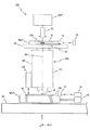


Classifications
-
- G—PHYSICS
- G03—PHOTOGRAPHY; CINEMATOGRAPHY; ANALOGOUS TECHNIQUES USING WAVES OTHER THAN OPTICAL WAVES; ELECTROGRAPHY; HOLOGRAPHY
- G03F—PHOTOMECHANICAL PRODUCTION OF TEXTURED OR PATTERNED SURFACES, e.g. FOR PRINTING, FOR PROCESSING OF SEMICONDUCTOR DEVICES; MATERIALS THEREFOR; ORIGINALS THEREFOR; APPARATUS SPECIALLY ADAPTED THEREFOR
- G03F7/00—Photomechanical, e.g. photolithographic, production of textured or patterned surfaces, e.g. printing surfaces; Materials therefor, e.g. comprising photoresists; Apparatus specially adapted therefor
- G03F7/70—Microphotolithographic exposure; Apparatus therefor
- G03F7/70483—Information management; Active and passive control; Testing; Wafer monitoring, e.g. pattern monitoring
- G03F7/7055—Exposure light control in all parts of the microlithographic apparatus, e.g. pulse length control or light interruption
- G03F7/70583—Speckle reduction, e.g. coherence control or amplitude/wavefront splitting
-
- G—PHYSICS
- G03—PHOTOGRAPHY; CINEMATOGRAPHY; ANALOGOUS TECHNIQUES USING WAVES OTHER THAN OPTICAL WAVES; ELECTROGRAPHY; HOLOGRAPHY
- G03F—PHOTOMECHANICAL PRODUCTION OF TEXTURED OR PATTERNED SURFACES, e.g. FOR PRINTING, FOR PROCESSING OF SEMICONDUCTOR DEVICES; MATERIALS THEREFOR; ORIGINALS THEREFOR; APPARATUS SPECIALLY ADAPTED THEREFOR
- G03F7/00—Photomechanical, e.g. photolithographic, production of textured or patterned surfaces, e.g. printing surfaces; Materials therefor, e.g. comprising photoresists; Apparatus specially adapted therefor
- G03F7/26—Processing photosensitive materials; Apparatus therefor
- G03F7/30—Imagewise removal using liquid means
- G03F7/32—Liquid compositions therefor, e.g. developers
-
- G—PHYSICS
- G03—PHOTOGRAPHY; CINEMATOGRAPHY; ANALOGOUS TECHNIQUES USING WAVES OTHER THAN OPTICAL WAVES; ELECTROGRAPHY; HOLOGRAPHY
- G03F—PHOTOMECHANICAL PRODUCTION OF TEXTURED OR PATTERNED SURFACES, e.g. FOR PRINTING, FOR PROCESSING OF SEMICONDUCTOR DEVICES; MATERIALS THEREFOR; ORIGINALS THEREFOR; APPARATUS SPECIALLY ADAPTED THEREFOR
- G03F7/00—Photomechanical, e.g. photolithographic, production of textured or patterned surfaces, e.g. printing surfaces; Materials therefor, e.g. comprising photoresists; Apparatus specially adapted therefor
- G03F7/70—Microphotolithographic exposure; Apparatus therefor
- G03F7/70216—Mask projection systems
- G03F7/70258—Projection system adjustments, e.g. adjustments during exposure or alignment during assembly of projection system
-
- G—PHYSICS
- G03—PHOTOGRAPHY; CINEMATOGRAPHY; ANALOGOUS TECHNIQUES USING WAVES OTHER THAN OPTICAL WAVES; ELECTROGRAPHY; HOLOGRAPHY
- G03F—PHOTOMECHANICAL PRODUCTION OF TEXTURED OR PATTERNED SURFACES, e.g. FOR PRINTING, FOR PROCESSING OF SEMICONDUCTOR DEVICES; MATERIALS THEREFOR; ORIGINALS THEREFOR; APPARATUS SPECIALLY ADAPTED THEREFOR
- G03F7/00—Photomechanical, e.g. photolithographic, production of textured or patterned surfaces, e.g. printing surfaces; Materials therefor, e.g. comprising photoresists; Apparatus specially adapted therefor
- G03F7/70—Microphotolithographic exposure; Apparatus therefor
- G03F7/70483—Information management; Active and passive control; Testing; Wafer monitoring, e.g. pattern monitoring
- G03F7/70491—Information management, e.g. software; Active and passive control, e.g. details of controlling exposure processes or exposure tool monitoring processes
- G03F7/70533—Controlling abnormal operating mode, e.g. taking account of waiting time, decision to rework or rework flow
-
- G—PHYSICS
- G03—PHOTOGRAPHY; CINEMATOGRAPHY; ANALOGOUS TECHNIQUES USING WAVES OTHER THAN OPTICAL WAVES; ELECTROGRAPHY; HOLOGRAPHY
- G03F—PHOTOMECHANICAL PRODUCTION OF TEXTURED OR PATTERNED SURFACES, e.g. FOR PRINTING, FOR PROCESSING OF SEMICONDUCTOR DEVICES; MATERIALS THEREFOR; ORIGINALS THEREFOR; APPARATUS SPECIALLY ADAPTED THEREFOR
- G03F7/00—Photomechanical, e.g. photolithographic, production of textured or patterned surfaces, e.g. printing surfaces; Materials therefor, e.g. comprising photoresists; Apparatus specially adapted therefor
- G03F7/70—Microphotolithographic exposure; Apparatus therefor
- G03F7/70483—Information management; Active and passive control; Testing; Wafer monitoring, e.g. pattern monitoring
- G03F7/70591—Testing optical components
- G03F7/706—Aberration measurement
-
- G—PHYSICS
- G03—PHOTOGRAPHY; CINEMATOGRAPHY; ANALOGOUS TECHNIQUES USING WAVES OTHER THAN OPTICAL WAVES; ELECTROGRAPHY; HOLOGRAPHY
- G03F—PHOTOMECHANICAL PRODUCTION OF TEXTURED OR PATTERNED SURFACES, e.g. FOR PRINTING, FOR PROCESSING OF SEMICONDUCTOR DEVICES; MATERIALS THEREFOR; ORIGINALS THEREFOR; APPARATUS SPECIALLY ADAPTED THEREFOR
- G03F7/00—Photomechanical, e.g. photolithographic, production of textured or patterned surfaces, e.g. printing surfaces; Materials therefor, e.g. comprising photoresists; Apparatus specially adapted therefor
- G03F7/70—Microphotolithographic exposure; Apparatus therefor
- G03F7/70483—Information management; Active and passive control; Testing; Wafer monitoring, e.g. pattern monitoring
- G03F7/70605—Workpiece metrology
- G03F7/70681—Metrology strategies
- G03F7/70683—Mark designs
-
- G—PHYSICS
- G03—PHOTOGRAPHY; CINEMATOGRAPHY; ANALOGOUS TECHNIQUES USING WAVES OTHER THAN OPTICAL WAVES; ELECTROGRAPHY; HOLOGRAPHY
- G03F—PHOTOMECHANICAL PRODUCTION OF TEXTURED OR PATTERNED SURFACES, e.g. FOR PRINTING, FOR PROCESSING OF SEMICONDUCTOR DEVICES; MATERIALS THEREFOR; ORIGINALS THEREFOR; APPARATUS SPECIALLY ADAPTED THEREFOR
- G03F7/00—Photomechanical, e.g. photolithographic, production of textured or patterned surfaces, e.g. printing surfaces; Materials therefor, e.g. comprising photoresists; Apparatus specially adapted therefor
- G03F7/70—Microphotolithographic exposure; Apparatus therefor
- G03F7/70483—Information management; Active and passive control; Testing; Wafer monitoring, e.g. pattern monitoring
- G03F7/70605—Workpiece metrology
- G03F7/706835—Metrology information management or control
-
- G—PHYSICS
- G03—PHOTOGRAPHY; CINEMATOGRAPHY; ANALOGOUS TECHNIQUES USING WAVES OTHER THAN OPTICAL WAVES; ELECTROGRAPHY; HOLOGRAPHY
- G03F—PHOTOMECHANICAL PRODUCTION OF TEXTURED OR PATTERNED SURFACES, e.g. FOR PRINTING, FOR PROCESSING OF SEMICONDUCTOR DEVICES; MATERIALS THEREFOR; ORIGINALS THEREFOR; APPARATUS SPECIALLY ADAPTED THEREFOR
- G03F7/00—Photomechanical, e.g. photolithographic, production of textured or patterned surfaces, e.g. printing surfaces; Materials therefor, e.g. comprising photoresists; Apparatus specially adapted therefor
- G03F7/70—Microphotolithographic exposure; Apparatus therefor
- G03F7/70483—Information management; Active and passive control; Testing; Wafer monitoring, e.g. pattern monitoring
- G03F7/70605—Workpiece metrology
- G03F7/706843—Metrology apparatus
- G03F7/706845—Calibration, e.g. tool-to-tool calibration, beam alignment, spot position or focus
-
- G—PHYSICS
- G03—PHOTOGRAPHY; CINEMATOGRAPHY; ANALOGOUS TECHNIQUES USING WAVES OTHER THAN OPTICAL WAVES; ELECTROGRAPHY; HOLOGRAPHY
- G03F—PHOTOMECHANICAL PRODUCTION OF TEXTURED OR PATTERNED SURFACES, e.g. FOR PRINTING, FOR PROCESSING OF SEMICONDUCTOR DEVICES; MATERIALS THEREFOR; ORIGINALS THEREFOR; APPARATUS SPECIALLY ADAPTED THEREFOR
- G03F7/00—Photomechanical, e.g. photolithographic, production of textured or patterned surfaces, e.g. printing surfaces; Materials therefor, e.g. comprising photoresists; Apparatus specially adapted therefor
- G03F7/70—Microphotolithographic exposure; Apparatus therefor
- G03F7/70691—Handling of masks or workpieces
- G03F7/70716—Stages
-
- G—PHYSICS
- G03—PHOTOGRAPHY; CINEMATOGRAPHY; ANALOGOUS TECHNIQUES USING WAVES OTHER THAN OPTICAL WAVES; ELECTROGRAPHY; HOLOGRAPHY
- G03F—PHOTOMECHANICAL PRODUCTION OF TEXTURED OR PATTERNED SURFACES, e.g. FOR PRINTING, FOR PROCESSING OF SEMICONDUCTOR DEVICES; MATERIALS THEREFOR; ORIGINALS THEREFOR; APPARATUS SPECIALLY ADAPTED THEREFOR
- G03F7/00—Photomechanical, e.g. photolithographic, production of textured or patterned surfaces, e.g. printing surfaces; Materials therefor, e.g. comprising photoresists; Apparatus specially adapted therefor
- G03F7/70—Microphotolithographic exposure; Apparatus therefor
- G03F7/70691—Handling of masks or workpieces
- G03F7/70775—Position control, e.g. interferometers or encoders for determining the stage position
-
- G—PHYSICS
- G03—PHOTOGRAPHY; CINEMATOGRAPHY; ANALOGOUS TECHNIQUES USING WAVES OTHER THAN OPTICAL WAVES; ELECTROGRAPHY; HOLOGRAPHY
- G03F—PHOTOMECHANICAL PRODUCTION OF TEXTURED OR PATTERNED SURFACES, e.g. FOR PRINTING, FOR PROCESSING OF SEMICONDUCTOR DEVICES; MATERIALS THEREFOR; ORIGINALS THEREFOR; APPARATUS SPECIALLY ADAPTED THEREFOR
- G03F7/00—Photomechanical, e.g. photolithographic, production of textured or patterned surfaces, e.g. printing surfaces; Materials therefor, e.g. comprising photoresists; Apparatus specially adapted therefor
- G03F7/70—Microphotolithographic exposure; Apparatus therefor
- G03F7/708—Construction of apparatus, e.g. environment aspects, hygiene aspects or materials
- G03F7/7085—Detection arrangement, e.g. detectors of apparatus alignment possibly mounted on wafers, exposure dose, photo-cleaning flux, stray light, thermal load
-
- G—PHYSICS
- G03—PHOTOGRAPHY; CINEMATOGRAPHY; ANALOGOUS TECHNIQUES USING WAVES OTHER THAN OPTICAL WAVES; ELECTROGRAPHY; HOLOGRAPHY
- G03F—PHOTOMECHANICAL PRODUCTION OF TEXTURED OR PATTERNED SURFACES, e.g. FOR PRINTING, FOR PROCESSING OF SEMICONDUCTOR DEVICES; MATERIALS THEREFOR; ORIGINALS THEREFOR; APPARATUS SPECIALLY ADAPTED THEREFOR
- G03F7/00—Photomechanical, e.g. photolithographic, production of textured or patterned surfaces, e.g. printing surfaces; Materials therefor, e.g. comprising photoresists; Apparatus specially adapted therefor
- G03F7/70—Microphotolithographic exposure; Apparatus therefor
- G03F7/708—Construction of apparatus, e.g. environment aspects, hygiene aspects or materials
- G03F7/70858—Environment aspects, e.g. pressure of beam-path gas, temperature
- G03F7/70866—Environment aspects, e.g. pressure of beam-path gas, temperature of mask or workpiece
- G03F7/70875—Temperature, e.g. temperature control of masks or workpieces via control of stage temperature
-
- G—PHYSICS
- G03—PHOTOGRAPHY; CINEMATOGRAPHY; ANALOGOUS TECHNIQUES USING WAVES OTHER THAN OPTICAL WAVES; ELECTROGRAPHY; HOLOGRAPHY
- G03F—PHOTOMECHANICAL PRODUCTION OF TEXTURED OR PATTERNED SURFACES, e.g. FOR PRINTING, FOR PROCESSING OF SEMICONDUCTOR DEVICES; MATERIALS THEREFOR; ORIGINALS THEREFOR; APPARATUS SPECIALLY ADAPTED THEREFOR
- G03F9/00—Registration or positioning of originals, masks, frames, photographic sheets or textured or patterned surfaces, e.g. automatically
- G03F9/70—Registration or positioning of originals, masks, frames, photographic sheets or textured or patterned surfaces, e.g. automatically for microlithography
- G03F9/7003—Alignment type or strategy, e.g. leveling, global alignment
- G03F9/7007—Alignment other than original with workpiece
- G03F9/7015—Reference, i.e. alignment of original or workpiece with respect to a reference not on the original or workpiece
-
- G—PHYSICS
- G03—PHOTOGRAPHY; CINEMATOGRAPHY; ANALOGOUS TECHNIQUES USING WAVES OTHER THAN OPTICAL WAVES; ELECTROGRAPHY; HOLOGRAPHY
- G03F—PHOTOMECHANICAL PRODUCTION OF TEXTURED OR PATTERNED SURFACES, e.g. FOR PRINTING, FOR PROCESSING OF SEMICONDUCTOR DEVICES; MATERIALS THEREFOR; ORIGINALS THEREFOR; APPARATUS SPECIALLY ADAPTED THEREFOR
- G03F9/00—Registration or positioning of originals, masks, frames, photographic sheets or textured or patterned surfaces, e.g. automatically
- G03F9/70—Registration or positioning of originals, masks, frames, photographic sheets or textured or patterned surfaces, e.g. automatically for microlithography
- G03F9/7088—Alignment mark detection, e.g. TTR, TTL, off-axis detection, array detector, video detection
Landscapes
- General Physics & Mathematics (AREA)
- Physics & Mathematics (AREA)
- Health & Medical Sciences (AREA)
- Engineering & Computer Science (AREA)
- Public Health (AREA)
- Environmental & Geological Engineering (AREA)
- Epidemiology (AREA)
- Toxicology (AREA)
- Atmospheric Sciences (AREA)
- Life Sciences & Earth Sciences (AREA)
- Multimedia (AREA)
- Exposure And Positioning Against Photoresist Photosensitive Materials (AREA)
- Length Measuring Devices By Optical Means (AREA)
Applications Claiming Priority (3)
| Application Number | Priority Date | Filing Date | Title |
|---|---|---|---|
| JP2014005684 | 2014-01-16 | ||
| JP2014005684 | 2014-01-16 | ||
| PCT/JP2015/050404 WO2015107976A1 (fr) | 2014-01-16 | 2015-01-08 | Appareil et procédé d'exposition et procédé de production du dispositif |
Related Child Applications (1)
| Application Number | Title | Priority Date | Filing Date |
|---|---|---|---|
| JP2018144707A Division JP2018173663A (ja) | 2014-01-16 | 2018-08-01 | 露光装置及び露光方法、並びにデバイス製造方法 |
Publications (2)
| Publication Number | Publication Date |
|---|---|
| JPWO2015107976A1 JPWO2015107976A1 (ja) | 2017-03-23 |
| JP6380412B2 true JP6380412B2 (ja) | 2018-08-29 |
Family
ID=53542866
Family Applications (2)
| Application Number | Title | Priority Date | Filing Date |
|---|---|---|---|
| JP2015557811A Active JP6380412B2 (ja) | 2014-01-16 | 2015-01-08 | 露光装置及び露光方法、並びにデバイス製造方法 |
| JP2018144707A Pending JP2018173663A (ja) | 2014-01-16 | 2018-08-01 | 露光装置及び露光方法、並びにデバイス製造方法 |
Family Applications After (1)
| Application Number | Title | Priority Date | Filing Date |
|---|---|---|---|
| JP2018144707A Pending JP2018173663A (ja) | 2014-01-16 | 2018-08-01 | 露光装置及び露光方法、並びにデバイス製造方法 |
Country Status (8)
| Country | Link |
|---|---|
| US (2) | US9915878B2 (fr) |
| EP (1) | EP3096346A4 (fr) |
| JP (2) | JP6380412B2 (fr) |
| KR (2) | KR20190032647A (fr) |
| CN (1) | CN105917441A (fr) |
| HK (1) | HK1225513A1 (fr) |
| TW (1) | TW201530264A (fr) |
| WO (1) | WO2015107976A1 (fr) |
Families Citing this family (11)
| Publication number | Priority date | Publication date | Assignee | Title |
|---|---|---|---|---|
| JP6572378B2 (ja) * | 2015-07-14 | 2019-09-11 | エーエスエムエル ネザーランズ ビー.ブイ. | リソグラフィ装置におけるパターニングデバイス冷却システム |
| JP6753934B2 (ja) | 2015-12-18 | 2020-09-09 | エーエスエムエル ネザーランズ ビー.ブイ. | 光学システムおよび方法 |
| JP6925783B2 (ja) * | 2016-05-26 | 2021-08-25 | 株式会社アドテックエンジニアリング | パターン描画装置及びパターン描画方法 |
| KR101971272B1 (ko) | 2016-06-02 | 2019-08-27 | 주식회사 더웨이브톡 | 패턴 구조물 검사 장치 및 검사 방법 |
| CN107883884B (zh) | 2016-09-30 | 2019-10-25 | 上海微电子装备(集团)股份有限公司 | 一种光学测量装置和方法 |
| CN107883887B (zh) | 2016-09-30 | 2019-11-26 | 上海微电子装备(集团)股份有限公司 | 一种光学测量装置和方法 |
| CN110337707B (zh) * | 2017-02-13 | 2021-09-28 | 株式会社日立高新技术 | 带电粒子线装置 |
| JP2022110461A (ja) * | 2021-01-18 | 2022-07-29 | 株式会社ニューフレアテクノロジー | 荷電粒子ビーム描画装置及びその調整方法 |
| JP7518782B2 (ja) * | 2021-02-19 | 2024-07-18 | キヤノン株式会社 | 計測装置、リソグラフィ装置、および物品の製造方法 |
| TWI776680B (zh) * | 2021-09-16 | 2022-09-01 | 日商新川股份有限公司 | 安裝裝置以及安裝裝置中的平行度檢測方法 |
| CN116960025A (zh) * | 2023-07-07 | 2023-10-27 | 武汉新芯集成电路制造有限公司 | 一种键合装置及键合方法 |
Family Cites Families (30)
| Publication number | Priority date | Publication date | Assignee | Title |
|---|---|---|---|---|
| US4780617A (en) | 1984-08-09 | 1988-10-25 | Nippon Kogaku K.K. | Method for successive alignment of chip patterns on a substrate |
| JPS6386429A (ja) * | 1986-09-30 | 1988-04-16 | Toshiba Corp | X線マスクのひずみ測定法 |
| JPH01230046A (ja) * | 1988-03-10 | 1989-09-13 | Toshiba Corp | 露光監視装置 |
| JP2787699B2 (ja) * | 1989-04-03 | 1998-08-20 | 株式会社ニコン | 干渉パターンの強度測定方法および露光装置 |
| JP3047461B2 (ja) * | 1990-11-26 | 2000-05-29 | 株式会社ニコン | 投影露光装置、投影露光方法、及び半導体集積回路製造方法 |
| KR100300618B1 (ko) | 1992-12-25 | 2001-11-22 | 오노 시게오 | 노광방법,노광장치,및그장치를사용하는디바이스제조방법 |
| JP3412704B2 (ja) | 1993-02-26 | 2003-06-03 | 株式会社ニコン | 投影露光方法及び装置、並びに露光装置 |
| JP3265503B2 (ja) * | 1993-06-11 | 2002-03-11 | 株式会社ニコン | 露光方法及び装置 |
| SG102627A1 (en) | 1996-11-28 | 2004-03-26 | Nikon Corp | Lithographic device |
| WO1998028665A1 (fr) | 1996-12-24 | 1998-07-02 | Koninklijke Philips Electronics N.V. | Dispositif de positionnement bidimensionnellement equilibre a deux porte-objets, et dispositif lithographique comportant ledit dispositif |
| JPH10247617A (ja) * | 1997-03-03 | 1998-09-14 | Nikon Corp | 投影露光方法及び投影露光装置 |
| US6208407B1 (en) | 1997-12-22 | 2001-03-27 | Asm Lithography B.V. | Method and apparatus for repetitively projecting a mask pattern on a substrate, using a time-saving height measurement |
| KR100841147B1 (ko) | 1998-03-11 | 2008-06-24 | 가부시키가이샤 니콘 | 레이저 장치, 자외광 조사 장치 및 방법, 물체의 패턴 검출장치 및 방법 |
| US6771350B2 (en) | 2000-02-25 | 2004-08-03 | Nikon Corporation | Exposure apparatus and exposure method capable of controlling illumination distribution |
| JP2002222761A (ja) * | 2000-11-22 | 2002-08-09 | Nikon Corp | 照明光学装置および該照明光学装置を備えた露光装置 |
| EP1364257A1 (fr) | 2001-02-27 | 2003-11-26 | ASML US, Inc. | Illustration simultanee de deux reticules |
| JP2003142365A (ja) * | 2001-10-31 | 2003-05-16 | Canon Inc | 露光装置及び露光方法 |
| JP2004165250A (ja) * | 2002-11-11 | 2004-06-10 | Nikon Corp | マスク検査方法、マスク検査装置、露光方法、及び露光装置 |
| KR100585476B1 (ko) | 2002-11-12 | 2006-06-07 | 에이에스엠엘 네델란즈 비.브이. | 리소그래피 장치 및 디바이스 제조방법 |
| EP1420298B1 (fr) | 2002-11-12 | 2013-02-20 | ASML Netherlands B.V. | Appareil lithographique |
| ATE424026T1 (de) | 2002-12-13 | 2009-03-15 | Koninkl Philips Electronics Nv | Flüssigkeitsentfernung in einem verfahren und einer einrichtung zum bestrahlen von flecken auf einer schicht |
| US6937349B2 (en) | 2003-05-02 | 2005-08-30 | Mitutoyo Corporation | Systems and methods for absolute positioning using repeated quasi-random pattern |
| JP2006019560A (ja) * | 2004-07-02 | 2006-01-19 | Canon Inc | 露光装置、走査型露光装置およびデバイス製造方法 |
| JP4545580B2 (ja) | 2004-12-27 | 2010-09-15 | 株式会社ミツトヨ | 面内方向変位計 |
| JP4817700B2 (ja) * | 2005-04-04 | 2011-11-16 | キヤノン株式会社 | 露光装置及び方法、並びに、デバイス製造方法 |
| JP5017556B2 (ja) * | 2007-03-19 | 2012-09-05 | 埼玉県 | 変形測定装置、変形測定方法および変形測定プログラム |
| US8994918B2 (en) * | 2010-10-21 | 2015-03-31 | Nikon Corporation | Apparatus and methods for measuring thermally induced reticle distortion |
| NL2007615A (en) * | 2010-11-30 | 2012-05-31 | Asml Netherlands Bv | Method of operating a patterning device and lithographic apparatus. |
| JP2013175541A (ja) * | 2012-02-24 | 2013-09-05 | Nikon Corp | マスク及びその変形量計測方法、並びに露光方法及び装置 |
| JP2013247258A (ja) * | 2012-05-28 | 2013-12-09 | Nikon Corp | アライメント方法、露光方法、及びデバイス製造方法、並びにデバイス製造システム |
-
2015
- 2015-01-08 JP JP2015557811A patent/JP6380412B2/ja active Active
- 2015-01-08 KR KR1020197008040A patent/KR20190032647A/ko not_active Withdrawn
- 2015-01-08 WO PCT/JP2015/050404 patent/WO2015107976A1/fr not_active Ceased
- 2015-01-08 HK HK16113798.9A patent/HK1225513A1/zh unknown
- 2015-01-08 KR KR1020167021913A patent/KR101963012B1/ko active Active
- 2015-01-08 EP EP15737108.9A patent/EP3096346A4/fr not_active Withdrawn
- 2015-01-08 CN CN201580004839.5A patent/CN105917441A/zh active Pending
- 2015-01-13 TW TW104101058A patent/TW201530264A/zh unknown
-
2016
- 2016-07-07 US US15/204,389 patent/US9915878B2/en active Active
-
2018
- 2018-01-03 US US15/861,000 patent/US20180143539A1/en not_active Abandoned
- 2018-08-01 JP JP2018144707A patent/JP2018173663A/ja active Pending
Also Published As
| Publication number | Publication date |
|---|---|
| US9915878B2 (en) | 2018-03-13 |
| JPWO2015107976A1 (ja) | 2017-03-23 |
| KR20160106733A (ko) | 2016-09-12 |
| EP3096346A1 (fr) | 2016-11-23 |
| WO2015107976A1 (fr) | 2015-07-23 |
| KR20190032647A (ko) | 2019-03-27 |
| KR101963012B1 (ko) | 2019-03-27 |
| JP2018173663A (ja) | 2018-11-08 |
| TW201530264A (zh) | 2015-08-01 |
| US20180143539A1 (en) | 2018-05-24 |
| EP3096346A4 (fr) | 2017-09-27 |
| US20160357116A1 (en) | 2016-12-08 |
| CN105917441A (zh) | 2016-08-31 |
| HK1225513A1 (zh) | 2017-09-08 |
Similar Documents
| Publication | Publication Date | Title |
|---|---|---|
| JP6380412B2 (ja) | 露光装置及び露光方法、並びにデバイス製造方法 | |
| US20250370360A1 (en) | Control method of movable body, exposure method, device manufacturing method, movable body apparatus, and exposure apparatus | |
| US10678152B2 (en) | Layout method, mark detection method, exposure method, measurement device, exposure apparatus, and device manufacturing method | |
| TW200305928A (en) | Exposure apparatus and method | |
| JP2002170754A (ja) | 露光装置、光学特性検出方法及び露光方法 | |
| JP5641210B2 (ja) | 露光装置、露光方法及びデバイス製造方法 | |
| JP5057235B2 (ja) | 較正方法、露光方法及びデバイス製造方法、並びに露光装置 | |
| US20140022377A1 (en) | Mark detection method, exposure method and exposure apparatus, and device manufacturing method | |
| JP6748907B2 (ja) | 計測装置、露光装置、デバイス製造方法、及びパターン形成方法 | |
| WO2016027477A1 (fr) | Appareil d'exposition, procédé d'exposition et procédé de fabrication d'un dispositif | |
| HK1229069A1 (en) | Exposure apparatus, exposure method, and device manufacturing method | |
| JP2014143229A (ja) | 計測方法及び計測システム、露光方法及び露光装置、並びにデバイス製造方法 | |
| JP2014096471A (ja) | 計測方法及び装置、照明方法及び装置、並びに露光方法及び装置 | |
| JP2007287898A (ja) | マーク部材、計測方法、計測装置及び露光装置 | |
| JP2016149405A (ja) | 計測装置、露光装置、デバイス製造方法、及び計測方法 | |
| JP2016143849A (ja) | 露光方法、デバイス製造方法、及び露光装置 | |
| JP2002043211A (ja) | アライメント装置及び露光装置 | |
| WO2016125790A1 (fr) | Dispositif de mesure et procédé de mesure, dispositif d'exposition et procédé d'exposition, et procédé de fabrication de dispositif | |
| HK1245500A1 (en) | Method for controlling moving body, exposure method, method for manufacturing device, moving body apparatus, and exposure apparatus |
Legal Events
| Date | Code | Title | Description |
|---|---|---|---|
| A131 | Notification of reasons for refusal |
Free format text: JAPANESE INTERMEDIATE CODE: A131 Effective date: 20170601 |
|
| A601 | Written request for extension of time |
Free format text: JAPANESE INTERMEDIATE CODE: A601 Effective date: 20170731 |
|
| A521 | Request for written amendment filed |
Free format text: JAPANESE INTERMEDIATE CODE: A523 Effective date: 20171002 |
|
| A131 | Notification of reasons for refusal |
Free format text: JAPANESE INTERMEDIATE CODE: A131 Effective date: 20180105 |
|
| A601 | Written request for extension of time |
Free format text: JAPANESE INTERMEDIATE CODE: A601 Effective date: 20180301 |
|
| A521 | Request for written amendment filed |
Free format text: JAPANESE INTERMEDIATE CODE: A523 Effective date: 20180501 |
|
| TRDD | Decision of grant or rejection written | ||
| A01 | Written decision to grant a patent or to grant a registration (utility model) |
Free format text: JAPANESE INTERMEDIATE CODE: A01 Effective date: 20180703 |
|
| A61 | First payment of annual fees (during grant procedure) |
Free format text: JAPANESE INTERMEDIATE CODE: A61 Effective date: 20180716 |
|
| R150 | Certificate of patent or registration of utility model |
Ref document number: 6380412 Country of ref document: JP Free format text: JAPANESE INTERMEDIATE CODE: R150 |
|
| R250 | Receipt of annual fees |
Free format text: JAPANESE INTERMEDIATE CODE: R250 |
|
| R250 | Receipt of annual fees |
Free format text: JAPANESE INTERMEDIATE CODE: R250 |
|
| R250 | Receipt of annual fees |
Free format text: JAPANESE INTERMEDIATE CODE: R250 |
|
| R250 | Receipt of annual fees |
Free format text: JAPANESE INTERMEDIATE CODE: R250 |
|
| R250 | Receipt of annual fees |
Free format text: JAPANESE INTERMEDIATE CODE: R250 |