JP7647239B2 - 半導体装置 - Google Patents
半導体装置 Download PDFInfo
- Publication number
- JP7647239B2 JP7647239B2 JP2021058100A JP2021058100A JP7647239B2 JP 7647239 B2 JP7647239 B2 JP 7647239B2 JP 2021058100 A JP2021058100 A JP 2021058100A JP 2021058100 A JP2021058100 A JP 2021058100A JP 7647239 B2 JP7647239 B2 JP 7647239B2
- Authority
- JP
- Japan
- Prior art keywords
- region
- layer
- gate
- base
- semiconductor device
- Prior art date
- Legal status (The legal status is an assumption and is not a legal conclusion. Google has not performed a legal analysis and makes no representation as to the accuracy of the status listed.)
- Active
Links
Images




Classifications
-
- H—ELECTRICITY
- H10—SEMICONDUCTOR DEVICES; ELECTRIC SOLID-STATE DEVICES NOT OTHERWISE PROVIDED FOR
- H10D—INORGANIC ELECTRIC SEMICONDUCTOR DEVICES
- H10D62/00—Semiconductor bodies, or regions thereof, of devices having potential barriers
- H10D62/10—Shapes, relative sizes or dispositions of the regions of the semiconductor bodies; Shapes of the semiconductor bodies
- H10D62/102—Constructional design considerations for preventing surface leakage or controlling electric field concentration
- H10D62/103—Constructional design considerations for preventing surface leakage or controlling electric field concentration for increasing or controlling the breakdown voltage of reverse-biased devices
- H10D62/105—Constructional design considerations for preventing surface leakage or controlling electric field concentration for increasing or controlling the breakdown voltage of reverse-biased devices by having particular doping profiles, shapes or arrangements of PN junctions; by having supplementary regions, e.g. junction termination extension [JTE]
- H10D62/109—Reduced surface field [RESURF] PN junction structures
-
- H—ELECTRICITY
- H10—SEMICONDUCTOR DEVICES; ELECTRIC SOLID-STATE DEVICES NOT OTHERWISE PROVIDED FOR
- H10D—INORGANIC ELECTRIC SEMICONDUCTOR DEVICES
- H10D12/00—Bipolar devices controlled by the field effect, e.g. insulated-gate bipolar transistors [IGBT]
- H10D12/01—Manufacture or treatment
- H10D12/031—Manufacture or treatment of IGBTs
-
- H—ELECTRICITY
- H10—SEMICONDUCTOR DEVICES; ELECTRIC SOLID-STATE DEVICES NOT OTHERWISE PROVIDED FOR
- H10D—INORGANIC ELECTRIC SEMICONDUCTOR DEVICES
- H10D12/00—Bipolar devices controlled by the field effect, e.g. insulated-gate bipolar transistors [IGBT]
- H10D12/01—Manufacture or treatment
- H10D12/031—Manufacture or treatment of IGBTs
- H10D12/032—Manufacture or treatment of IGBTs of vertical IGBTs
- H10D12/038—Manufacture or treatment of IGBTs of vertical IGBTs having a recessed gate, e.g. trench-gate IGBTs
-
- H—ELECTRICITY
- H10—SEMICONDUCTOR DEVICES; ELECTRIC SOLID-STATE DEVICES NOT OTHERWISE PROVIDED FOR
- H10D—INORGANIC ELECTRIC SEMICONDUCTOR DEVICES
- H10D30/00—Field-effect transistors [FET]
- H10D30/01—Manufacture or treatment
- H10D30/021—Manufacture or treatment of FETs having insulated gates [IGFET]
- H10D30/028—Manufacture or treatment of FETs having insulated gates [IGFET] of double-diffused metal oxide semiconductor [DMOS] FETs
- H10D30/0291—Manufacture or treatment of FETs having insulated gates [IGFET] of double-diffused metal oxide semiconductor [DMOS] FETs of vertical DMOS [VDMOS] FETs
- H10D30/0297—Manufacture or treatment of FETs having insulated gates [IGFET] of double-diffused metal oxide semiconductor [DMOS] FETs of vertical DMOS [VDMOS] FETs using recessing of the gate electrodes, e.g. to form trench gate electrodes
-
- H—ELECTRICITY
- H10—SEMICONDUCTOR DEVICES; ELECTRIC SOLID-STATE DEVICES NOT OTHERWISE PROVIDED FOR
- H10D—INORGANIC ELECTRIC SEMICONDUCTOR DEVICES
- H10D30/00—Field-effect transistors [FET]
- H10D30/60—Insulated-gate field-effect transistors [IGFET]
- H10D30/64—Double-diffused metal-oxide semiconductor [DMOS] FETs
- H10D30/66—Vertical DMOS [VDMOS] FETs
- H10D30/665—Vertical DMOS [VDMOS] FETs having edge termination structures
-
- H—ELECTRICITY
- H10—SEMICONDUCTOR DEVICES; ELECTRIC SOLID-STATE DEVICES NOT OTHERWISE PROVIDED FOR
- H10D—INORGANIC ELECTRIC SEMICONDUCTOR DEVICES
- H10D30/00—Field-effect transistors [FET]
- H10D30/60—Insulated-gate field-effect transistors [IGFET]
- H10D30/64—Double-diffused metal-oxide semiconductor [DMOS] FETs
- H10D30/66—Vertical DMOS [VDMOS] FETs
- H10D30/668—Vertical DMOS [VDMOS] FETs having trench gate electrodes, e.g. UMOS transistors
-
- H—ELECTRICITY
- H10—SEMICONDUCTOR DEVICES; ELECTRIC SOLID-STATE DEVICES NOT OTHERWISE PROVIDED FOR
- H10D—INORGANIC ELECTRIC SEMICONDUCTOR DEVICES
- H10D62/00—Semiconductor bodies, or regions thereof, of devices having potential barriers
- H10D62/10—Shapes, relative sizes or dispositions of the regions of the semiconductor bodies; Shapes of the semiconductor bodies
- H10D62/102—Constructional design considerations for preventing surface leakage or controlling electric field concentration
- H10D62/103—Constructional design considerations for preventing surface leakage or controlling electric field concentration for increasing or controlling the breakdown voltage of reverse-biased devices
- H10D62/104—Constructional design considerations for preventing surface leakage or controlling electric field concentration for increasing or controlling the breakdown voltage of reverse-biased devices having particular shapes of the bodies at or near reverse-biased junctions, e.g. having bevels or moats
-
- H—ELECTRICITY
- H10—SEMICONDUCTOR DEVICES; ELECTRIC SOLID-STATE DEVICES NOT OTHERWISE PROVIDED FOR
- H10D—INORGANIC ELECTRIC SEMICONDUCTOR DEVICES
- H10D62/00—Semiconductor bodies, or regions thereof, of devices having potential barriers
- H10D62/10—Shapes, relative sizes or dispositions of the regions of the semiconductor bodies; Shapes of the semiconductor bodies
- H10D62/102—Constructional design considerations for preventing surface leakage or controlling electric field concentration
- H10D62/103—Constructional design considerations for preventing surface leakage or controlling electric field concentration for increasing or controlling the breakdown voltage of reverse-biased devices
- H10D62/105—Constructional design considerations for preventing surface leakage or controlling electric field concentration for increasing or controlling the breakdown voltage of reverse-biased devices by having particular doping profiles, shapes or arrangements of PN junctions; by having supplementary regions, e.g. junction termination extension [JTE]
- H10D62/106—Constructional design considerations for preventing surface leakage or controlling electric field concentration for increasing or controlling the breakdown voltage of reverse-biased devices by having particular doping profiles, shapes or arrangements of PN junctions; by having supplementary regions, e.g. junction termination extension [JTE] having supplementary regions doped oppositely to or in rectifying contact with regions of the semiconductor bodies, e.g. guard rings with PN or Schottky junctions
- H10D62/107—Buried supplementary regions, e.g. buried guard rings
-
- H—ELECTRICITY
- H10—SEMICONDUCTOR DEVICES; ELECTRIC SOLID-STATE DEVICES NOT OTHERWISE PROVIDED FOR
- H10D—INORGANIC ELECTRIC SEMICONDUCTOR DEVICES
- H10D62/00—Semiconductor bodies, or regions thereof, of devices having potential barriers
- H10D62/10—Shapes, relative sizes or dispositions of the regions of the semiconductor bodies; Shapes of the semiconductor bodies
- H10D62/13—Semiconductor regions connected to electrodes carrying current to be rectified, amplified or switched, e.g. source or drain regions
- H10D62/149—Source or drain regions of field-effect devices
- H10D62/151—Source or drain regions of field-effect devices of IGFETs
- H10D62/156—Drain regions of DMOS transistors
- H10D62/157—Impurity concentrations or distributions
-
- H—ELECTRICITY
- H10—SEMICONDUCTOR DEVICES; ELECTRIC SOLID-STATE DEVICES NOT OTHERWISE PROVIDED FOR
- H10D—INORGANIC ELECTRIC SEMICONDUCTOR DEVICES
- H10D62/00—Semiconductor bodies, or regions thereof, of devices having potential barriers
- H10D62/10—Shapes, relative sizes or dispositions of the regions of the semiconductor bodies; Shapes of the semiconductor bodies
- H10D62/17—Semiconductor regions connected to electrodes not carrying current to be rectified, amplified or switched, e.g. channel regions
- H10D62/393—Body regions of DMOS transistors or IGBTs
-
- H—ELECTRICITY
- H10—SEMICONDUCTOR DEVICES; ELECTRIC SOLID-STATE DEVICES NOT OTHERWISE PROVIDED FOR
- H10D—INORGANIC ELECTRIC SEMICONDUCTOR DEVICES
- H10D62/00—Semiconductor bodies, or regions thereof, of devices having potential barriers
- H10D62/80—Semiconductor bodies, or regions thereof, of devices having potential barriers characterised by the materials
- H10D62/83—Semiconductor bodies, or regions thereof, of devices having potential barriers characterised by the materials being Group IV materials, e.g. B-doped Si or undoped Ge
- H10D62/832—Semiconductor bodies, or regions thereof, of devices having potential barriers characterised by the materials being Group IV materials, e.g. B-doped Si or undoped Ge being Group IV materials comprising two or more elements, e.g. SiGe
- H10D62/8325—Silicon carbide
-
- H—ELECTRICITY
- H10—SEMICONDUCTOR DEVICES; ELECTRIC SOLID-STATE DEVICES NOT OTHERWISE PROVIDED FOR
- H10P—GENERIC PROCESSES OR APPARATUS FOR THE MANUFACTURE OR TREATMENT OF DEVICES COVERED BY CLASS H10
- H10P30/00—Ion implantation into wafers, substrates or parts of devices
- H10P30/20—Ion implantation into wafers, substrates or parts of devices into semiconductor materials, e.g. for doping
- H10P30/22—Ion implantation into wafers, substrates or parts of devices into semiconductor materials, e.g. for doping using masks
-
- H—ELECTRICITY
- H10—SEMICONDUCTOR DEVICES; ELECTRIC SOLID-STATE DEVICES NOT OTHERWISE PROVIDED FOR
- H10W—GENERIC PACKAGES, INTERCONNECTIONS, CONNECTORS OR OTHER CONSTRUCTIONAL DETAILS OF DEVICES COVERED BY CLASS H10
- H10W10/00—Isolation regions in semiconductor bodies between components of integrated devices
-
- H—ELECTRICITY
- H10—SEMICONDUCTOR DEVICES; ELECTRIC SOLID-STATE DEVICES NOT OTHERWISE PROVIDED FOR
- H10W—GENERIC PACKAGES, INTERCONNECTIONS, CONNECTORS OR OTHER CONSTRUCTIONAL DETAILS OF DEVICES COVERED BY CLASS H10
- H10W10/00—Isolation regions in semiconductor bodies between components of integrated devices
- H10W10/01—Manufacture or treatment
-
- H—ELECTRICITY
- H10—SEMICONDUCTOR DEVICES; ELECTRIC SOLID-STATE DEVICES NOT OTHERWISE PROVIDED FOR
- H10W—GENERIC PACKAGES, INTERCONNECTIONS, CONNECTORS OR OTHER CONSTRUCTIONAL DETAILS OF DEVICES COVERED BY CLASS H10
- H10W10/00—Isolation regions in semiconductor bodies between components of integrated devices
- H10W10/01—Manufacture or treatment
- H10W10/031—Manufacture or treatment of isolation regions comprising PN junctions
-
- H—ELECTRICITY
- H10—SEMICONDUCTOR DEVICES; ELECTRIC SOLID-STATE DEVICES NOT OTHERWISE PROVIDED FOR
- H10W—GENERIC PACKAGES, INTERCONNECTIONS, CONNECTORS OR OTHER CONSTRUCTIONAL DETAILS OF DEVICES COVERED BY CLASS H10
- H10W10/00—Isolation regions in semiconductor bodies between components of integrated devices
- H10W10/30—Isolation regions comprising PN junctions
-
- H—ELECTRICITY
- H10—SEMICONDUCTOR DEVICES; ELECTRIC SOLID-STATE DEVICES NOT OTHERWISE PROVIDED FOR
- H10D—INORGANIC ELECTRIC SEMICONDUCTOR DEVICES
- H10D62/00—Semiconductor bodies, or regions thereof, of devices having potential barriers
- H10D62/10—Shapes, relative sizes or dispositions of the regions of the semiconductor bodies; Shapes of the semiconductor bodies
- H10D62/102—Constructional design considerations for preventing surface leakage or controlling electric field concentration
- H10D62/103—Constructional design considerations for preventing surface leakage or controlling electric field concentration for increasing or controlling the breakdown voltage of reverse-biased devices
- H10D62/105—Constructional design considerations for preventing surface leakage or controlling electric field concentration for increasing or controlling the breakdown voltage of reverse-biased devices by having particular doping profiles, shapes or arrangements of PN junctions; by having supplementary regions, e.g. junction termination extension [JTE]
- H10D62/106—Constructional design considerations for preventing surface leakage or controlling electric field concentration for increasing or controlling the breakdown voltage of reverse-biased devices by having particular doping profiles, shapes or arrangements of PN junctions; by having supplementary regions, e.g. junction termination extension [JTE] having supplementary regions doped oppositely to or in rectifying contact with regions of the semiconductor bodies, e.g. guard rings with PN or Schottky junctions
-
- H—ELECTRICITY
- H10—SEMICONDUCTOR DEVICES; ELECTRIC SOLID-STATE DEVICES NOT OTHERWISE PROVIDED FOR
- H10D—INORGANIC ELECTRIC SEMICONDUCTOR DEVICES
- H10D62/00—Semiconductor bodies, or regions thereof, of devices having potential barriers
- H10D62/10—Shapes, relative sizes or dispositions of the regions of the semiconductor bodies; Shapes of the semiconductor bodies
- H10D62/102—Constructional design considerations for preventing surface leakage or controlling electric field concentration
- H10D62/112—Constructional design considerations for preventing surface leakage or controlling electric field concentration for preventing surface leakage due to surface inversion layers, e.g. by using channel stoppers
-
- H—ELECTRICITY
- H10—SEMICONDUCTOR DEVICES; ELECTRIC SOLID-STATE DEVICES NOT OTHERWISE PROVIDED FOR
- H10D—INORGANIC ELECTRIC SEMICONDUCTOR DEVICES
- H10D62/00—Semiconductor bodies, or regions thereof, of devices having potential barriers
- H10D62/80—Semiconductor bodies, or regions thereof, of devices having potential barriers characterised by the materials
- H10D62/85—Semiconductor bodies, or regions thereof, of devices having potential barriers characterised by the materials being Group III-V materials, e.g. GaAs
- H10D62/8503—Nitride Group III-V materials, e.g. AlN or GaN
Landscapes
- Insulated Gate Type Field-Effect Transistor (AREA)
- Electrodes Of Semiconductors (AREA)
Description
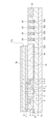
本発明の実施形態に係るSiC半導体装置(半導体チップ)100は、図1に示すように、活性部101と外周部102とからなる。例えば、活性部101は矩形状の平面形状を有し、外周部102は活性部101を囲んでその周辺に配置される。図2は、図1に示したA-A線方向から見た断面図である。図2に示すように、活性部101には活性素子が含まれ、外周部102には終端構造が含まれる。図2では、活性素子として第1導電型(n-型)のドリフト層2の上部に設けられたトレンチゲート構造のMOSFETを、終端構造として複数の電界緩和領域(ガードリング)44を含む場合を例示している。ストライプ状のトレンチ11aは紙面に垂直な方向に延在する。
次に、図6~図18の工程断面図を用いて、実施形態に係るSiC半導体装置の製造方法を、トレンチ型MOSFETの場合を一例に説明する。なお、以下に述べるトレンチ型MOSFETの製造方法は一例であり、特許請求の範囲に記載した趣旨の範囲であれば、この変形例を含めて、これ以外の種々の製造方法により実現可能であることは勿論である。
上記のように、本発明の実施形態に係る絶縁ゲート型半導体装置を記載したが、この開示の一部をなす論述及び図面は本発明を限定するものであると理解すべきではない。この開示から当業者には様々な代替実施形態、実施例及び運用技術が明らかとなろう。
1p…半導体基板(基板)
2…ドリフト層
3…第1拡散層
(3,6)…電流拡散層
4,4a…第1埋込領域
(4,7)…ベース底部埋込領域
4r…下端部(第2下端部)
4x…注入領域
4xr…下端部
5…ゲート底部保護領域
5r…下端部(第1下端部)
5s…上端部
6…第2拡散層
7,7a…第2埋込領域
8…ベース領域
9…ソース領域(第1主領域)
10…ベースコンタクト領域
11a…トレンチ
(11a、14a)…絶縁ゲート型電極構造
11b…メサ溝
12…フィールド酸化膜
13…ゲート絶縁膜
14a…ゲート電極
15…層間絶縁膜
16…ソースコンタクト層
17…バリアメタル層
18a…ソース電極(第1主電極)
19…ドレイン電極(第2主電極)
22、22a、42a…部分電流拡散層
33…チャネルストッパ
44…電界緩和領域(ガードリング)
Claims (8)
- シリコンよりもバンドギャップが広い六方晶系半導体からなる第1導電型のドリフト層と、
前記ドリフト層の上面に設けられ、前記ドリフト層より高不純物濃度の第1導電型の電流拡散層と、
前記電流拡散層の上面に設けられた第2導電型のベース領域と、
前記電流拡散層の内部に設けられ、曲面からなる第1下端部を有する第2導電型のゲート底部保護領域と、
前記電流拡散層の内部に前記ゲート底部保護領域と離間して、前記ベース領域の下面に接し、前記ゲート底部保護領域に対向する側面に、曲面からなる第2下端部を有する第2導電型のベース底部埋込領域と、
前記ベース領域を貫通し前記ゲート底部保護領域に達するストライプ状のトレンチの内部に設けられた絶縁ゲート型電極構造と、
を備え、
前記トレンチの延在方向に垂直に切った断面において、
前記ベース底部埋込領域の底面が、前記ゲート底部保護領域の底面より深くに位置し、
前記第1下端部の曲率半径の最小値が、前記第2下端部の曲率半径の最小値より大きいことを特徴とする半導体装置。 - 前記ゲート底部保護領域が、前記ベース底部埋込領域よりも高不純物濃度を有することを特徴とする請求項1に記載の半導体装置。
- 前記ゲート底部保護領域の不純物濃度が3×1018cm-3以上1×1019cm-3未満であることを特徴とする請求項1又は2に記載の半導体装置。
- 前記ベース底部埋込領域の不純物濃度が1×1017cm-3以上3×1018cm-3未満であることを特徴とする請求項1又は2に記載の半導体装置。
- 前記ゲート底部保護領域が曲面からなる上端部を有し、該上端部の曲率半径の最小値は前記第2下端部の前記曲率半径の最小値よりも大きいことを特徴とする請求項1~4のいずれか1項に記載の半導体装置。
- 前記ベース底部埋込領域の前記底面に接し、前記電流拡散層よりも高不純物濃度の第1導電型の部分電流拡散層を更に備えることを特徴とする請求項1~5のいずれか1項に記載の半導体装置。
- 前記絶縁ゲート型電極構造が設けられた活性部の周囲に配置され、前記ドリフト層の上部に底面が前記ベース底部埋込領域の前記底面と同一レベルで、前記ベース底部埋込領域と同一不純物濃度で設けられた第2導電型のガードリングを更に備えることを特徴とする請求項1~6のいずれか1項に記載の半導体装置。
- 前記六方晶系半導体が、炭化珪素であることを特徴とする請求項1~7のいずれか1項に記載の半導体装置。
Priority Applications (2)
| Application Number | Priority Date | Filing Date | Title |
|---|---|---|---|
| JP2021058100A JP7647239B2 (ja) | 2021-03-30 | 2021-03-30 | 半導体装置 |
| US17/587,753 US12068366B2 (en) | 2021-03-30 | 2022-01-28 | Semiconductor device |
Applications Claiming Priority (1)
| Application Number | Priority Date | Filing Date | Title |
|---|---|---|---|
| JP2021058100A JP7647239B2 (ja) | 2021-03-30 | 2021-03-30 | 半導体装置 |
Publications (2)
| Publication Number | Publication Date |
|---|---|
| JP2022154849A JP2022154849A (ja) | 2022-10-13 |
| JP7647239B2 true JP7647239B2 (ja) | 2025-03-18 |
Family
ID=83449087
Family Applications (1)
| Application Number | Title | Priority Date | Filing Date |
|---|---|---|---|
| JP2021058100A Active JP7647239B2 (ja) | 2021-03-30 | 2021-03-30 | 半導体装置 |
Country Status (2)
| Country | Link |
|---|---|
| US (1) | US12068366B2 (ja) |
| JP (1) | JP7647239B2 (ja) |
Families Citing this family (7)
| Publication number | Priority date | Publication date | Assignee | Title |
|---|---|---|---|---|
| EP4145533A4 (en) * | 2020-12-24 | 2024-05-01 | Fuji Electric Co., Ltd. | INSULATED GATE TYPE SEMICONDUCTOR DEVICE |
| IT202300003897A1 (it) * | 2023-03-03 | 2024-09-03 | St Microelectronics Int Nv | Procedimento di fabbricazione di un dispositivo elettronico di potenza dotato di uno strato di diffusione corrente |
| JP2024132527A (ja) * | 2023-03-17 | 2024-10-01 | 株式会社東芝 | 半導体装置 |
| JP2024137537A (ja) * | 2023-03-24 | 2024-10-07 | 株式会社東芝 | 半導体装置 |
| JP2024157941A (ja) * | 2023-04-26 | 2024-11-08 | 株式会社デンソー | 炭化珪素半導体装置 |
| US12154941B1 (en) | 2024-01-18 | 2024-11-26 | Diodes Incorporated | Power MOSFET with gate-source ESD diode structure |
| WO2025224813A1 (ja) * | 2024-04-23 | 2025-10-30 | 三菱電機株式会社 | 半導体装置及び半導体装置の製造方法 |
Citations (4)
| Publication number | Priority date | Publication date | Assignee | Title |
|---|---|---|---|---|
| WO2015049838A1 (ja) | 2013-10-02 | 2015-04-09 | 株式会社デンソー | 炭化珪素半導体装置 |
| US20180166530A1 (en) | 2016-12-08 | 2018-06-14 | Cree, Inc. | Power semiconductor devices having gate trenches and buried edge terminations and related methods |
| US20180358463A1 (en) | 2017-06-09 | 2018-12-13 | Fuji Electric Co., Ltd. | Semiconductor device and method of manufacturing a semiconductor device |
| US20200403066A1 (en) | 2019-06-21 | 2020-12-24 | Fuji Electric Co., Ltd. | Semiconductor device |
Family Cites Families (6)
| Publication number | Priority date | Publication date | Assignee | Title |
|---|---|---|---|---|
| CN105474402B (zh) | 2013-08-01 | 2018-09-04 | 三菱电机株式会社 | 碳化硅半导体器件及其制造方法 |
| JP6409681B2 (ja) | 2015-05-29 | 2018-10-24 | 株式会社デンソー | 半導体装置およびその製造方法 |
| CN108352402B (zh) | 2015-10-16 | 2020-12-18 | 富士电机株式会社 | 半导体装置和半导体装置的制造方法 |
| JP6617657B2 (ja) | 2016-07-29 | 2019-12-11 | 富士電機株式会社 | 炭化ケイ素半導体装置および炭化ケイ素半導体装置の製造方法 |
| JP6870546B2 (ja) | 2017-09-14 | 2021-05-12 | 株式会社デンソー | 半導体装置およびその製造方法 |
| JP7098906B2 (ja) | 2017-10-11 | 2022-07-12 | 株式会社デンソー | ショットキーバリアダイオードを備えた炭化珪素半導体装置およびその製造方法 |
-
2021
- 2021-03-30 JP JP2021058100A patent/JP7647239B2/ja active Active
-
2022
- 2022-01-28 US US17/587,753 patent/US12068366B2/en active Active
Patent Citations (7)
| Publication number | Priority date | Publication date | Assignee | Title |
|---|---|---|---|---|
| WO2015049838A1 (ja) | 2013-10-02 | 2015-04-09 | 株式会社デンソー | 炭化珪素半導体装置 |
| US20180166530A1 (en) | 2016-12-08 | 2018-06-14 | Cree, Inc. | Power semiconductor devices having gate trenches and buried edge terminations and related methods |
| JP2021048423A (ja) | 2016-12-08 | 2021-03-25 | クリー インコーポレイテッドCree Inc. | ゲート・トレンチと、埋め込まれた終端構造とを有するパワー半導体デバイス、及び、関連方法 |
| US20180358463A1 (en) | 2017-06-09 | 2018-12-13 | Fuji Electric Co., Ltd. | Semiconductor device and method of manufacturing a semiconductor device |
| JP2019003968A (ja) | 2017-06-09 | 2019-01-10 | 国立研究開発法人産業技術総合研究所 | 半導体装置および半導体装置の製造方法 |
| US20200403066A1 (en) | 2019-06-21 | 2020-12-24 | Fuji Electric Co., Ltd. | Semiconductor device |
| JP2021002597A (ja) | 2019-06-21 | 2021-01-07 | 富士電機株式会社 | 半導体装置 |
Also Published As
| Publication number | Publication date |
|---|---|
| US20220320268A1 (en) | 2022-10-06 |
| JP2022154849A (ja) | 2022-10-13 |
| US12068366B2 (en) | 2024-08-20 |
Similar Documents
| Publication | Publication Date | Title |
|---|---|---|
| JP7647239B2 (ja) | 半導体装置 | |
| JP7563526B2 (ja) | 絶縁ゲート型半導体装置の製造方法 | |
| JP7697553B2 (ja) | 半導体装置及びその製造方法 | |
| US8618557B2 (en) | Wide-band-gap reverse-blocking MOS-type semiconductor device | |
| JP6946764B2 (ja) | 半導体装置および半導体装置の製造方法 | |
| JP5773073B2 (ja) | 半導体装置 | |
| JP7622449B2 (ja) | 半導体装置 | |
| JP7459975B2 (ja) | 絶縁ゲート型半導体装置 | |
| JP7625903B2 (ja) | 絶縁ゲート型半導体装置 | |
| JP7703882B2 (ja) | 炭化珪素半導体装置及びその製造方法 | |
| JP2019106507A (ja) | 炭化シリコン半導体装置及びその製造方法 | |
| JP7544152B2 (ja) | 絶縁ゲート型半導体装置 | |
| US20190140095A1 (en) | Semiconductor device | |
| JP2017092355A (ja) | 半導体装置および半導体装置の製造方法 | |
| JP7768317B2 (ja) | 半導体装置 | |
| US12272746B2 (en) | Semiconductor device | |
| US12002873B2 (en) | Method for adjusting groove depth and method for manufacturing semiconductor device | |
| US20240072132A1 (en) | Semiconductor device and method of manufacturing the same | |
| JP2024125068A (ja) | 炭化珪素半導体装置及びその製造方法 | |
| JP2017092364A (ja) | 半導体装置および半導体装置の製造方法 | |
| US12615794B2 (en) | Semiconductor device and method of manufacturing the same | |
| JP2024148334A (ja) | 炭化珪素半導体装置及びその製造方法 | |
| JP7731660B2 (ja) | 半導体装置および半導体装置の製造方法 | |
| JP2024125067A (ja) | 炭化珪素半導体装置及びその製造方法 | |
| US20250380440A1 (en) | Insulated gate semiconductor device |
Legal Events
| Date | Code | Title | Description |
|---|---|---|---|
| A621 | Written request for application examination |
Free format text: JAPANESE INTERMEDIATE CODE: A621 Effective date: 20240313 |
|
| A977 | Report on retrieval |
Free format text: JAPANESE INTERMEDIATE CODE: A971007 Effective date: 20241216 |
|
| TRDD | Decision of grant or rejection written | ||
| A01 | Written decision to grant a patent or to grant a registration (utility model) |
Free format text: JAPANESE INTERMEDIATE CODE: A01 Effective date: 20250204 |
|
| A61 | First payment of annual fees (during grant procedure) |
Free format text: JAPANESE INTERMEDIATE CODE: A61 Effective date: 20250217 |
|
| R150 | Certificate of patent or registration of utility model |
Ref document number: 7647239 Country of ref document: JP Free format text: JAPANESE INTERMEDIATE CODE: R150 |