JP7648246B2 - 薄膜トランジスタ - Google Patents
薄膜トランジスタ Download PDFInfo
- Publication number
- JP7648246B2 JP7648246B2 JP2024020841A JP2024020841A JP7648246B2 JP 7648246 B2 JP7648246 B2 JP 7648246B2 JP 2024020841 A JP2024020841 A JP 2024020841A JP 2024020841 A JP2024020841 A JP 2024020841A JP 7648246 B2 JP7648246 B2 JP 7648246B2
- Authority
- JP
- Japan
- Prior art keywords
- region
- layer
- pixel
- conductive layer
- gate electrode
- Prior art date
- Legal status (The legal status is an assumption and is not a legal conclusion. Google has not performed a legal analysis and makes no representation as to the accuracy of the status listed.)
- Active
Links
Images


Classifications
-
- G—PHYSICS
- G02—OPTICS
- G02F—OPTICAL DEVICES OR ARRANGEMENTS FOR THE CONTROL OF LIGHT BY MODIFICATION OF THE OPTICAL PROPERTIES OF THE MEDIA OF THE ELEMENTS INVOLVED THEREIN; NON-LINEAR OPTICS; FREQUENCY-CHANGING OF LIGHT; OPTICAL LOGIC ELEMENTS; OPTICAL ANALOGUE/DIGITAL CONVERTERS
- G02F1/00—Devices or arrangements for the control of the intensity, colour, phase, polarisation or direction of light arriving from an independent light source, e.g. switching, gating or modulating; Non-linear optics
- G02F1/01—Devices or arrangements for the control of the intensity, colour, phase, polarisation or direction of light arriving from an independent light source, e.g. switching, gating or modulating; Non-linear optics for the control of the intensity, phase, polarisation or colour
- G02F1/13—Devices or arrangements for the control of the intensity, colour, phase, polarisation or direction of light arriving from an independent light source, e.g. switching, gating or modulating; Non-linear optics for the control of the intensity, phase, polarisation or colour based on liquid crystals, e.g. single liquid crystal display cells
- G02F1/133—Constructional arrangements; Operation of liquid crystal cells; Circuit arrangements
- G02F1/136—Liquid crystal cells structurally associated with a semi-conducting layer or substrate, e.g. cells forming part of an integrated circuit
- G02F1/1362—Active matrix addressed cells
- G02F1/1368—Active matrix addressed cells in which the switching element is a three-electrode device
-
- G—PHYSICS
- G02—OPTICS
- G02F—OPTICAL DEVICES OR ARRANGEMENTS FOR THE CONTROL OF LIGHT BY MODIFICATION OF THE OPTICAL PROPERTIES OF THE MEDIA OF THE ELEMENTS INVOLVED THEREIN; NON-LINEAR OPTICS; FREQUENCY-CHANGING OF LIGHT; OPTICAL LOGIC ELEMENTS; OPTICAL ANALOGUE/DIGITAL CONVERTERS
- G02F1/00—Devices or arrangements for the control of the intensity, colour, phase, polarisation or direction of light arriving from an independent light source, e.g. switching, gating or modulating; Non-linear optics
- G02F1/01—Devices or arrangements for the control of the intensity, colour, phase, polarisation or direction of light arriving from an independent light source, e.g. switching, gating or modulating; Non-linear optics for the control of the intensity, phase, polarisation or colour
- G02F1/13—Devices or arrangements for the control of the intensity, colour, phase, polarisation or direction of light arriving from an independent light source, e.g. switching, gating or modulating; Non-linear optics for the control of the intensity, phase, polarisation or colour based on liquid crystals, e.g. single liquid crystal display cells
- G02F1/133—Constructional arrangements; Operation of liquid crystal cells; Circuit arrangements
- G02F1/1333—Constructional arrangements; Manufacturing methods
- G02F1/1339—Gaskets; Spacers; Sealing of cells
-
- G—PHYSICS
- G02—OPTICS
- G02F—OPTICAL DEVICES OR ARRANGEMENTS FOR THE CONTROL OF LIGHT BY MODIFICATION OF THE OPTICAL PROPERTIES OF THE MEDIA OF THE ELEMENTS INVOLVED THEREIN; NON-LINEAR OPTICS; FREQUENCY-CHANGING OF LIGHT; OPTICAL LOGIC ELEMENTS; OPTICAL ANALOGUE/DIGITAL CONVERTERS
- G02F1/00—Devices or arrangements for the control of the intensity, colour, phase, polarisation or direction of light arriving from an independent light source, e.g. switching, gating or modulating; Non-linear optics
- G02F1/01—Devices or arrangements for the control of the intensity, colour, phase, polarisation or direction of light arriving from an independent light source, e.g. switching, gating or modulating; Non-linear optics for the control of the intensity, phase, polarisation or colour
- G02F1/13—Devices or arrangements for the control of the intensity, colour, phase, polarisation or direction of light arriving from an independent light source, e.g. switching, gating or modulating; Non-linear optics for the control of the intensity, phase, polarisation or colour based on liquid crystals, e.g. single liquid crystal display cells
- G02F1/133—Constructional arrangements; Operation of liquid crystal cells; Circuit arrangements
- G02F1/1333—Constructional arrangements; Manufacturing methods
- G02F1/1343—Electrodes
- G02F1/134309—Electrodes characterised by their geometrical arrangement
-
- G—PHYSICS
- G02—OPTICS
- G02F—OPTICAL DEVICES OR ARRANGEMENTS FOR THE CONTROL OF LIGHT BY MODIFICATION OF THE OPTICAL PROPERTIES OF THE MEDIA OF THE ELEMENTS INVOLVED THEREIN; NON-LINEAR OPTICS; FREQUENCY-CHANGING OF LIGHT; OPTICAL LOGIC ELEMENTS; OPTICAL ANALOGUE/DIGITAL CONVERTERS
- G02F1/00—Devices or arrangements for the control of the intensity, colour, phase, polarisation or direction of light arriving from an independent light source, e.g. switching, gating or modulating; Non-linear optics
- G02F1/01—Devices or arrangements for the control of the intensity, colour, phase, polarisation or direction of light arriving from an independent light source, e.g. switching, gating or modulating; Non-linear optics for the control of the intensity, phase, polarisation or colour
- G02F1/13—Devices or arrangements for the control of the intensity, colour, phase, polarisation or direction of light arriving from an independent light source, e.g. switching, gating or modulating; Non-linear optics for the control of the intensity, phase, polarisation or colour based on liquid crystals, e.g. single liquid crystal display cells
- G02F1/133—Constructional arrangements; Operation of liquid crystal cells; Circuit arrangements
- G02F1/1333—Constructional arrangements; Manufacturing methods
- G02F1/1343—Electrodes
- G02F1/13439—Electrodes characterised by their electrical, optical, physical properties; materials therefor; method of making
-
- G—PHYSICS
- G02—OPTICS
- G02F—OPTICAL DEVICES OR ARRANGEMENTS FOR THE CONTROL OF LIGHT BY MODIFICATION OF THE OPTICAL PROPERTIES OF THE MEDIA OF THE ELEMENTS INVOLVED THEREIN; NON-LINEAR OPTICS; FREQUENCY-CHANGING OF LIGHT; OPTICAL LOGIC ELEMENTS; OPTICAL ANALOGUE/DIGITAL CONVERTERS
- G02F1/00—Devices or arrangements for the control of the intensity, colour, phase, polarisation or direction of light arriving from an independent light source, e.g. switching, gating or modulating; Non-linear optics
- G02F1/01—Devices or arrangements for the control of the intensity, colour, phase, polarisation or direction of light arriving from an independent light source, e.g. switching, gating or modulating; Non-linear optics for the control of the intensity, phase, polarisation or colour
- G02F1/13—Devices or arrangements for the control of the intensity, colour, phase, polarisation or direction of light arriving from an independent light source, e.g. switching, gating or modulating; Non-linear optics for the control of the intensity, phase, polarisation or colour based on liquid crystals, e.g. single liquid crystal display cells
- G02F1/133—Constructional arrangements; Operation of liquid crystal cells; Circuit arrangements
- G02F1/1333—Constructional arrangements; Manufacturing methods
- G02F1/1345—Conductors connecting electrodes to cell terminals
-
- G—PHYSICS
- G02—OPTICS
- G02F—OPTICAL DEVICES OR ARRANGEMENTS FOR THE CONTROL OF LIGHT BY MODIFICATION OF THE OPTICAL PROPERTIES OF THE MEDIA OF THE ELEMENTS INVOLVED THEREIN; NON-LINEAR OPTICS; FREQUENCY-CHANGING OF LIGHT; OPTICAL LOGIC ELEMENTS; OPTICAL ANALOGUE/DIGITAL CONVERTERS
- G02F1/00—Devices or arrangements for the control of the intensity, colour, phase, polarisation or direction of light arriving from an independent light source, e.g. switching, gating or modulating; Non-linear optics
- G02F1/01—Devices or arrangements for the control of the intensity, colour, phase, polarisation or direction of light arriving from an independent light source, e.g. switching, gating or modulating; Non-linear optics for the control of the intensity, phase, polarisation or colour
- G02F1/13—Devices or arrangements for the control of the intensity, colour, phase, polarisation or direction of light arriving from an independent light source, e.g. switching, gating or modulating; Non-linear optics for the control of the intensity, phase, polarisation or colour based on liquid crystals, e.g. single liquid crystal display cells
- G02F1/133—Constructional arrangements; Operation of liquid crystal cells; Circuit arrangements
- G02F1/136—Liquid crystal cells structurally associated with a semi-conducting layer or substrate, e.g. cells forming part of an integrated circuit
- G02F1/1362—Active matrix addressed cells
- G02F1/136209—Light shielding layers, e.g. black matrix, incorporated in the active matrix substrate, e.g. structurally associated with the switching element
-
- G—PHYSICS
- G02—OPTICS
- G02F—OPTICAL DEVICES OR ARRANGEMENTS FOR THE CONTROL OF LIGHT BY MODIFICATION OF THE OPTICAL PROPERTIES OF THE MEDIA OF THE ELEMENTS INVOLVED THEREIN; NON-LINEAR OPTICS; FREQUENCY-CHANGING OF LIGHT; OPTICAL LOGIC ELEMENTS; OPTICAL ANALOGUE/DIGITAL CONVERTERS
- G02F1/00—Devices or arrangements for the control of the intensity, colour, phase, polarisation or direction of light arriving from an independent light source, e.g. switching, gating or modulating; Non-linear optics
- G02F1/01—Devices or arrangements for the control of the intensity, colour, phase, polarisation or direction of light arriving from an independent light source, e.g. switching, gating or modulating; Non-linear optics for the control of the intensity, phase, polarisation or colour
- G02F1/13—Devices or arrangements for the control of the intensity, colour, phase, polarisation or direction of light arriving from an independent light source, e.g. switching, gating or modulating; Non-linear optics for the control of the intensity, phase, polarisation or colour based on liquid crystals, e.g. single liquid crystal display cells
- G02F1/133—Constructional arrangements; Operation of liquid crystal cells; Circuit arrangements
- G02F1/136—Liquid crystal cells structurally associated with a semi-conducting layer or substrate, e.g. cells forming part of an integrated circuit
- G02F1/1362—Active matrix addressed cells
- G02F1/136227—Through-hole connection of the pixel electrode to the active element through an insulation layer
-
- G—PHYSICS
- G02—OPTICS
- G02F—OPTICAL DEVICES OR ARRANGEMENTS FOR THE CONTROL OF LIGHT BY MODIFICATION OF THE OPTICAL PROPERTIES OF THE MEDIA OF THE ELEMENTS INVOLVED THEREIN; NON-LINEAR OPTICS; FREQUENCY-CHANGING OF LIGHT; OPTICAL LOGIC ELEMENTS; OPTICAL ANALOGUE/DIGITAL CONVERTERS
- G02F1/00—Devices or arrangements for the control of the intensity, colour, phase, polarisation or direction of light arriving from an independent light source, e.g. switching, gating or modulating; Non-linear optics
- G02F1/01—Devices or arrangements for the control of the intensity, colour, phase, polarisation or direction of light arriving from an independent light source, e.g. switching, gating or modulating; Non-linear optics for the control of the intensity, phase, polarisation or colour
- G02F1/13—Devices or arrangements for the control of the intensity, colour, phase, polarisation or direction of light arriving from an independent light source, e.g. switching, gating or modulating; Non-linear optics for the control of the intensity, phase, polarisation or colour based on liquid crystals, e.g. single liquid crystal display cells
- G02F1/133—Constructional arrangements; Operation of liquid crystal cells; Circuit arrangements
- G02F1/136—Liquid crystal cells structurally associated with a semi-conducting layer or substrate, e.g. cells forming part of an integrated circuit
- G02F1/1362—Active matrix addressed cells
- G02F1/136286—Wiring, e.g. gate line, drain line
- G02F1/13629—Multilayer wirings
-
- H—ELECTRICITY
- H10—SEMICONDUCTOR DEVICES; ELECTRIC SOLID-STATE DEVICES NOT OTHERWISE PROVIDED FOR
- H10D—INORGANIC ELECTRIC SEMICONDUCTOR DEVICES
- H10D30/00—Field-effect transistors [FET]
- H10D30/60—Insulated-gate field-effect transistors [IGFET]
- H10D30/67—Thin-film transistors [TFT]
- H10D30/6729—Thin-film transistors [TFT] characterised by the electrodes
- H10D30/673—Thin-film transistors [TFT] characterised by the electrodes characterised by the shapes, relative sizes or dispositions of the gate electrodes
- H10D30/6733—Multi-gate TFTs
- H10D30/6734—Multi-gate TFTs having gate electrodes arranged on both top and bottom sides of the channel, e.g. dual-gate TFTs
-
- H—ELECTRICITY
- H10—SEMICONDUCTOR DEVICES; ELECTRIC SOLID-STATE DEVICES NOT OTHERWISE PROVIDED FOR
- H10D—INORGANIC ELECTRIC SEMICONDUCTOR DEVICES
- H10D30/00—Field-effect transistors [FET]
- H10D30/60—Insulated-gate field-effect transistors [IGFET]
- H10D30/67—Thin-film transistors [TFT]
- H10D30/674—Thin-film transistors [TFT] characterised by the active materials
- H10D30/6755—Oxide semiconductors, e.g. zinc oxide, copper aluminium oxide or cadmium stannate
-
- H—ELECTRICITY
- H10—SEMICONDUCTOR DEVICES; ELECTRIC SOLID-STATE DEVICES NOT OTHERWISE PROVIDED FOR
- H10D—INORGANIC ELECTRIC SEMICONDUCTOR DEVICES
- H10D86/00—Integrated devices formed in or on insulating or conducting substrates, e.g. formed in silicon-on-insulator [SOI] substrates or on stainless steel or glass substrates
- H10D86/40—Integrated devices formed in or on insulating or conducting substrates, e.g. formed in silicon-on-insulator [SOI] substrates or on stainless steel or glass substrates characterised by multiple TFTs
- H10D86/421—Integrated devices formed in or on insulating or conducting substrates, e.g. formed in silicon-on-insulator [SOI] substrates or on stainless steel or glass substrates characterised by multiple TFTs having a particular composition, shape or crystalline structure of the active layer
- H10D86/423—Integrated devices formed in or on insulating or conducting substrates, e.g. formed in silicon-on-insulator [SOI] substrates or on stainless steel or glass substrates characterised by multiple TFTs having a particular composition, shape or crystalline structure of the active layer comprising semiconductor materials not belonging to the Group IV, e.g. InGaZnO
-
- H—ELECTRICITY
- H10—SEMICONDUCTOR DEVICES; ELECTRIC SOLID-STATE DEVICES NOT OTHERWISE PROVIDED FOR
- H10D—INORGANIC ELECTRIC SEMICONDUCTOR DEVICES
- H10D86/00—Integrated devices formed in or on insulating or conducting substrates, e.g. formed in silicon-on-insulator [SOI] substrates or on stainless steel or glass substrates
- H10D86/40—Integrated devices formed in or on insulating or conducting substrates, e.g. formed in silicon-on-insulator [SOI] substrates or on stainless steel or glass substrates characterised by multiple TFTs
- H10D86/441—Interconnections, e.g. scanning lines
- H10D86/443—Interconnections, e.g. scanning lines adapted for preventing breakage, peeling or short circuiting
-
- H—ELECTRICITY
- H10—SEMICONDUCTOR DEVICES; ELECTRIC SOLID-STATE DEVICES NOT OTHERWISE PROVIDED FOR
- H10D—INORGANIC ELECTRIC SEMICONDUCTOR DEVICES
- H10D86/00—Integrated devices formed in or on insulating or conducting substrates, e.g. formed in silicon-on-insulator [SOI] substrates or on stainless steel or glass substrates
- H10D86/40—Integrated devices formed in or on insulating or conducting substrates, e.g. formed in silicon-on-insulator [SOI] substrates or on stainless steel or glass substrates characterised by multiple TFTs
- H10D86/60—Integrated devices formed in or on insulating or conducting substrates, e.g. formed in silicon-on-insulator [SOI] substrates or on stainless steel or glass substrates characterised by multiple TFTs wherein the TFTs are in active matrices
-
- G—PHYSICS
- G02—OPTICS
- G02F—OPTICAL DEVICES OR ARRANGEMENTS FOR THE CONTROL OF LIGHT BY MODIFICATION OF THE OPTICAL PROPERTIES OF THE MEDIA OF THE ELEMENTS INVOLVED THEREIN; NON-LINEAR OPTICS; FREQUENCY-CHANGING OF LIGHT; OPTICAL LOGIC ELEMENTS; OPTICAL ANALOGUE/DIGITAL CONVERTERS
- G02F1/00—Devices or arrangements for the control of the intensity, colour, phase, polarisation or direction of light arriving from an independent light source, e.g. switching, gating or modulating; Non-linear optics
- G02F1/01—Devices or arrangements for the control of the intensity, colour, phase, polarisation or direction of light arriving from an independent light source, e.g. switching, gating or modulating; Non-linear optics for the control of the intensity, phase, polarisation or colour
- G02F1/13—Devices or arrangements for the control of the intensity, colour, phase, polarisation or direction of light arriving from an independent light source, e.g. switching, gating or modulating; Non-linear optics for the control of the intensity, phase, polarisation or colour based on liquid crystals, e.g. single liquid crystal display cells
- G02F1/133—Constructional arrangements; Operation of liquid crystal cells; Circuit arrangements
- G02F1/1333—Constructional arrangements; Manufacturing methods
- G02F1/1337—Surface-induced orientation of the liquid crystal molecules, e.g. by alignment layers
- G02F1/133707—Structures for producing distorted electric fields, e.g. bumps, protrusions, recesses, slits in pixel electrodes
-
- G—PHYSICS
- G02—OPTICS
- G02F—OPTICAL DEVICES OR ARRANGEMENTS FOR THE CONTROL OF LIGHT BY MODIFICATION OF THE OPTICAL PROPERTIES OF THE MEDIA OF THE ELEMENTS INVOLVED THEREIN; NON-LINEAR OPTICS; FREQUENCY-CHANGING OF LIGHT; OPTICAL LOGIC ELEMENTS; OPTICAL ANALOGUE/DIGITAL CONVERTERS
- G02F1/00—Devices or arrangements for the control of the intensity, colour, phase, polarisation or direction of light arriving from an independent light source, e.g. switching, gating or modulating; Non-linear optics
- G02F1/01—Devices or arrangements for the control of the intensity, colour, phase, polarisation or direction of light arriving from an independent light source, e.g. switching, gating or modulating; Non-linear optics for the control of the intensity, phase, polarisation or colour
- G02F1/13—Devices or arrangements for the control of the intensity, colour, phase, polarisation or direction of light arriving from an independent light source, e.g. switching, gating or modulating; Non-linear optics for the control of the intensity, phase, polarisation or colour based on liquid crystals, e.g. single liquid crystal display cells
- G02F1/133—Constructional arrangements; Operation of liquid crystal cells; Circuit arrangements
- G02F1/1333—Constructional arrangements; Manufacturing methods
- G02F1/1345—Conductors connecting electrodes to cell terminals
- G02F1/13452—Conductors connecting driver circuitry and terminals of panels
-
- G—PHYSICS
- G02—OPTICS
- G02F—OPTICAL DEVICES OR ARRANGEMENTS FOR THE CONTROL OF LIGHT BY MODIFICATION OF THE OPTICAL PROPERTIES OF THE MEDIA OF THE ELEMENTS INVOLVED THEREIN; NON-LINEAR OPTICS; FREQUENCY-CHANGING OF LIGHT; OPTICAL LOGIC ELEMENTS; OPTICAL ANALOGUE/DIGITAL CONVERTERS
- G02F1/00—Devices or arrangements for the control of the intensity, colour, phase, polarisation or direction of light arriving from an independent light source, e.g. switching, gating or modulating; Non-linear optics
- G02F1/01—Devices or arrangements for the control of the intensity, colour, phase, polarisation or direction of light arriving from an independent light source, e.g. switching, gating or modulating; Non-linear optics for the control of the intensity, phase, polarisation or colour
- G02F1/13—Devices or arrangements for the control of the intensity, colour, phase, polarisation or direction of light arriving from an independent light source, e.g. switching, gating or modulating; Non-linear optics for the control of the intensity, phase, polarisation or colour based on liquid crystals, e.g. single liquid crystal display cells
- G02F1/133—Constructional arrangements; Operation of liquid crystal cells; Circuit arrangements
- G02F1/1333—Constructional arrangements; Manufacturing methods
- G02F1/1345—Conductors connecting electrodes to cell terminals
- G02F1/13458—Terminal pads
-
- G—PHYSICS
- G02—OPTICS
- G02F—OPTICAL DEVICES OR ARRANGEMENTS FOR THE CONTROL OF LIGHT BY MODIFICATION OF THE OPTICAL PROPERTIES OF THE MEDIA OF THE ELEMENTS INVOLVED THEREIN; NON-LINEAR OPTICS; FREQUENCY-CHANGING OF LIGHT; OPTICAL LOGIC ELEMENTS; OPTICAL ANALOGUE/DIGITAL CONVERTERS
- G02F1/00—Devices or arrangements for the control of the intensity, colour, phase, polarisation or direction of light arriving from an independent light source, e.g. switching, gating or modulating; Non-linear optics
- G02F1/01—Devices or arrangements for the control of the intensity, colour, phase, polarisation or direction of light arriving from an independent light source, e.g. switching, gating or modulating; Non-linear optics for the control of the intensity, phase, polarisation or colour
- G02F1/13—Devices or arrangements for the control of the intensity, colour, phase, polarisation or direction of light arriving from an independent light source, e.g. switching, gating or modulating; Non-linear optics for the control of the intensity, phase, polarisation or colour based on liquid crystals, e.g. single liquid crystal display cells
- G02F1/133—Constructional arrangements; Operation of liquid crystal cells; Circuit arrangements
- G02F1/136—Liquid crystal cells structurally associated with a semi-conducting layer or substrate, e.g. cells forming part of an integrated circuit
- G02F1/1362—Active matrix addressed cells
- G02F1/136231—Active matrix addressed cells for reducing the number of lithographic steps
- G02F1/136236—Active matrix addressed cells for reducing the number of lithographic steps using a grey or half tone lithographic process
-
- G—PHYSICS
- G02—OPTICS
- G02F—OPTICAL DEVICES OR ARRANGEMENTS FOR THE CONTROL OF LIGHT BY MODIFICATION OF THE OPTICAL PROPERTIES OF THE MEDIA OF THE ELEMENTS INVOLVED THEREIN; NON-LINEAR OPTICS; FREQUENCY-CHANGING OF LIGHT; OPTICAL LOGIC ELEMENTS; OPTICAL ANALOGUE/DIGITAL CONVERTERS
- G02F1/00—Devices or arrangements for the control of the intensity, colour, phase, polarisation or direction of light arriving from an independent light source, e.g. switching, gating or modulating; Non-linear optics
- G02F1/01—Devices or arrangements for the control of the intensity, colour, phase, polarisation or direction of light arriving from an independent light source, e.g. switching, gating or modulating; Non-linear optics for the control of the intensity, phase, polarisation or colour
- G02F1/13—Devices or arrangements for the control of the intensity, colour, phase, polarisation or direction of light arriving from an independent light source, e.g. switching, gating or modulating; Non-linear optics for the control of the intensity, phase, polarisation or colour based on liquid crystals, e.g. single liquid crystal display cells
- G02F1/133—Constructional arrangements; Operation of liquid crystal cells; Circuit arrangements
- G02F1/136—Liquid crystal cells structurally associated with a semi-conducting layer or substrate, e.g. cells forming part of an integrated circuit
- G02F1/1362—Active matrix addressed cells
- G02F1/1368—Active matrix addressed cells in which the switching element is a three-electrode device
- G02F1/13685—Top gates
-
- G—PHYSICS
- G02—OPTICS
- G02F—OPTICAL DEVICES OR ARRANGEMENTS FOR THE CONTROL OF LIGHT BY MODIFICATION OF THE OPTICAL PROPERTIES OF THE MEDIA OF THE ELEMENTS INVOLVED THEREIN; NON-LINEAR OPTICS; FREQUENCY-CHANGING OF LIGHT; OPTICAL LOGIC ELEMENTS; OPTICAL ANALOGUE/DIGITAL CONVERTERS
- G02F2201/00—Constructional arrangements not provided for in groups G02F1/00 - G02F7/00
- G02F2201/40—Arrangements for improving the aperture ratio
-
- G—PHYSICS
- G09—EDUCATION; CRYPTOGRAPHY; DISPLAY; ADVERTISING; SEALS
- G09G—ARRANGEMENTS OR CIRCUITS FOR CONTROL OF INDICATING DEVICES USING STATIC MEANS TO PRESENT VARIABLE INFORMATION
- G09G2300/00—Aspects of the constitution of display devices
- G09G2300/04—Structural and physical details of display devices
- G09G2300/0404—Matrix technologies
- G09G2300/0417—Special arrangements specific to the use of low carrier mobility technology
-
- G—PHYSICS
- G09—EDUCATION; CRYPTOGRAPHY; DISPLAY; ADVERTISING; SEALS
- G09G—ARRANGEMENTS OR CIRCUITS FOR CONTROL OF INDICATING DEVICES USING STATIC MEANS TO PRESENT VARIABLE INFORMATION
- G09G2300/00—Aspects of the constitution of display devices
- G09G2300/04—Structural and physical details of display devices
- G09G2300/0421—Structural details of the set of electrodes
- G09G2300/0426—Layout of electrodes and connections
-
- G—PHYSICS
- G09—EDUCATION; CRYPTOGRAPHY; DISPLAY; ADVERTISING; SEALS
- G09G—ARRANGEMENTS OR CIRCUITS FOR CONTROL OF INDICATING DEVICES USING STATIC MEANS TO PRESENT VARIABLE INFORMATION
- G09G2310/00—Command of the display device
- G09G2310/02—Addressing, scanning or driving the display screen or processing steps related thereto
- G09G2310/0264—Details of driving circuits
- G09G2310/0297—Special arrangements with multiplexing or demultiplexing of display data in the drivers for data electrodes, in a pre-processing circuitry delivering display data to said drivers or in the matrix panel, e.g. multiplexing plural data signals to one D/A converter or demultiplexing the D/A converter output to multiple columns
-
- G—PHYSICS
- G09—EDUCATION; CRYPTOGRAPHY; DISPLAY; ADVERTISING; SEALS
- G09G—ARRANGEMENTS OR CIRCUITS FOR CONTROL OF INDICATING DEVICES USING STATIC MEANS TO PRESENT VARIABLE INFORMATION
- G09G3/00—Control arrangements or circuits, of interest only in connection with visual indicators other than cathode-ray tubes
- G09G3/20—Control arrangements or circuits, of interest only in connection with visual indicators other than cathode-ray tubes for presentation of an assembly of a number of characters, e.g. a page, by composing the assembly by combination of individual elements arranged in a matrix no fixed position being assigned to or needed to be assigned to the individual characters or partial characters
- G09G3/34—Control arrangements or circuits, of interest only in connection with visual indicators other than cathode-ray tubes for presentation of an assembly of a number of characters, e.g. a page, by composing the assembly by combination of individual elements arranged in a matrix no fixed position being assigned to or needed to be assigned to the individual characters or partial characters by control of light from an independent source
- G09G3/36—Control arrangements or circuits, of interest only in connection with visual indicators other than cathode-ray tubes for presentation of an assembly of a number of characters, e.g. a page, by composing the assembly by combination of individual elements arranged in a matrix no fixed position being assigned to or needed to be assigned to the individual characters or partial characters by control of light from an independent source using liquid crystals
- G09G3/3611—Control of matrices with row and column drivers
- G09G3/3614—Control of polarity reversal in general
-
- G—PHYSICS
- G09—EDUCATION; CRYPTOGRAPHY; DISPLAY; ADVERTISING; SEALS
- G09G—ARRANGEMENTS OR CIRCUITS FOR CONTROL OF INDICATING DEVICES USING STATIC MEANS TO PRESENT VARIABLE INFORMATION
- G09G3/00—Control arrangements or circuits, of interest only in connection with visual indicators other than cathode-ray tubes
- G09G3/20—Control arrangements or circuits, of interest only in connection with visual indicators other than cathode-ray tubes for presentation of an assembly of a number of characters, e.g. a page, by composing the assembly by combination of individual elements arranged in a matrix no fixed position being assigned to or needed to be assigned to the individual characters or partial characters
- G09G3/34—Control arrangements or circuits, of interest only in connection with visual indicators other than cathode-ray tubes for presentation of an assembly of a number of characters, e.g. a page, by composing the assembly by combination of individual elements arranged in a matrix no fixed position being assigned to or needed to be assigned to the individual characters or partial characters by control of light from an independent source
- G09G3/36—Control arrangements or circuits, of interest only in connection with visual indicators other than cathode-ray tubes for presentation of an assembly of a number of characters, e.g. a page, by composing the assembly by combination of individual elements arranged in a matrix no fixed position being assigned to or needed to be assigned to the individual characters or partial characters by control of light from an independent source using liquid crystals
- G09G3/3611—Control of matrices with row and column drivers
- G09G3/3648—Control of matrices with row and column drivers using an active matrix
- G09G3/3655—Details of drivers for counter electrodes, e.g. common electrodes for pixel capacitors or supplementary storage capacitors
Landscapes
- Physics & Mathematics (AREA)
- Nonlinear Science (AREA)
- Mathematical Physics (AREA)
- Chemical & Material Sciences (AREA)
- Crystallography & Structural Chemistry (AREA)
- General Physics & Mathematics (AREA)
- Optics & Photonics (AREA)
- Engineering & Computer Science (AREA)
- Microelectronics & Electronic Packaging (AREA)
- Geometry (AREA)
- Liquid Crystal (AREA)
- Thin Film Transistor (AREA)
Description
縁層との間の第1画素電極と、第2絶縁層上の第2画素電極と、を含む。トランジスタは、第1絶縁層と酸化物半導体層との間に配置され、第1ゲート電極及び第2ゲート電極を挟むように配置される第1酸化物導電層と第2酸化物導電層とをさらに含み、第1画素電極と第2画素電極とは、第2酸化物導電層から連続する配線と電気的に接続され、第1ゲート電極と第2ゲート電極とは、酸化物半導体層の外側の領域で、第1絶縁層及び第2絶縁層を貫通する第1コンタクトホールによって電気的に接続されている。
本発明の一実施形態に係る液晶表示装置の回路構成について示す。以下においては、FFS(Fringe Field Switching)方式及びIPS(In Plane Switching)方式に適用可能な回路構成、及びPSVA(Polymer Stabilized Vertical Alignment)方式に適用可能
な回路構成について例示する。
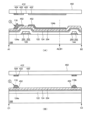
図1は、本発明の一実施形態に係るFFS方式及びIPS方式の液晶表示装置200aの構成を示す。液晶表示装置200aは、対向して配置された第1基板100と第2基板102との間に液晶層(図示されず)が設けられた構造を有し、液晶の電気光学効果を利用して画像が表示される表示部104を備えている。表示部104は、少なくとも1つの画素106、走査信号線116、コモン信号線117、データ信号線118が配設される。少なくとも1つの画素106は、複数の画素から成る。複数の画素106は、表示部104に適宜配列されている。複数の画素106は、例えば、ストライプ配列、モザイク配列、デルタ配列、ペンタイル配列に対応するように配置される。
8、コモン信号線駆動回路109、データ信号線駆動回路110が適宜配置され得る。表示部104に配設される走査信号線116は走査信号線駆動回路108と接続され、コモン信号線117はコモン信号線駆動回路109と接続され、データ信号線118はデータ信号線駆動回路110と接続される。走査信号線駆動回路108は走査信号線116に走査信号を出力し、コモン信号線駆動回路109はコモン信号線117にコモン信号を出力し、データ信号線駆動回路110はデータ信号線118に映像信号を出力する。
線118との関係において、画素106(nRm)、106(nGm)、106(n+1Rm)、106(n+1Gm)が第m列目に対応して配置された第1データ信号線118(Dm)と接続され、画素106(nBm+1)、106(nRm+1)、106(n+1Bm+1)、106(n+1Rm+1)が第m+1列目に対応して配置された第2データ信号線118(Dm+1)と接続される。また、第n行目に配置された画素は、コモン電極が第1コモン信号線117(COMn)と接続され、第n+1行目に配置された画素はコモン電極が第2コモン信号線(COMn+1)と接続される。
図5は、本発明の一実施形態に係るPSVA方式の液晶表示装置200bの構成を示す。液晶表示装置200bは、対向して配置された第1基板100と第2基板102との間に液晶層(図示されず)が設けられた構造を有し、液晶の電気光学効果を利用して画像が表示される表示部104を備えている。液晶表示装置200aは、また、表示部104の
外側の領域に走査信号線駆動回路108、データ信号線駆動回路110が適宜配置されている。表示部104に配設される走査信号線116は走査信号線駆動回路108と接続され、データ信号線118はデータ信号線駆動回路110と接続される。走査信号線駆動回路108は走査信号線116に走査信号を出力し、データ信号線駆動回路110はデータ信号線118に映像信号を出力する。液晶素子204及び保持容量素子206の一方の端子はトランジスタ202と電気的に接続され、他方の端子にはコモン電圧が印加される。
トランジスタ202は、チャネル領域が半導体薄膜で形成される薄膜トランジスタである。トランジスタ202は、走査信号線116及びデータ信号線118と共に、フォトリソフグラフィによる微細パターン作成技術を用いて作製される。液晶表示装置200a、200bの製造コストを低減するためには、フォトマスクの数を削減することが必要と考えられている。しかし、走査信号線116及びデータ信号線118は交差して配置する必要がある。また、これらの配線の一部は、液晶層をシールするシールパターンと交差するように設ける必要がある。走査信号線116及びデータ信号線118は金属配線で形成されるが、シールパターンと重なる部分では金属配線を露出させることができないため、配線を無機絶縁膜で被覆することが必要とされている。シール材と金属配線とが直接接していると、シール材と金属配線との界面を通して大気中の水分(H2O)が液晶層に浸透しやすくなり、信頼性を低下させる原因となる。
本発明の一実施形態に係る液晶表示装置200a、200bに用いられるトランジスタ202の詳細を説明する。本実施形態においてトランジスタ202は薄膜トランジスタであり、以下に示すように少なくとも2種類の構造を有している。
図7(A)及び図7(B)は、トランジスタの第1の構造例を示す。図7(A)は、トランジスタ202の平面図を示す。図7(B)は、図7(A)に示すX1-X2線に対応する、トランジスタ202の断面構造を示す。
酸化物半導体層128は、元素として、インジウム(In)、亜鉛(Zn)、ガリウム(Ga)、スズ(Sn)、アルミニウム(Al)、マグネシウム(Mg)から選ばれた一種又は複数種を含む。例えば、酸化物半導体層128を形成する酸化物半導体材料としては、半導体特性を示す、三元系酸化物材料、二元系酸化物材料、及び一元系酸化物材料を用いることができる。四元系酸化物材料としては、In2O3-Ga2O3-SnO2-ZnO系酸化物材料が例示される。三元系酸化物材料としては、In2O3-Ga2O3-ZnO系酸化物材料、In2O3-SnO2-ZnO系酸化物材料、In2O3-Al2O3-ZnO系酸化物材料、Ga2O3-SnO2-ZnO系酸化物材料、Ga2O3-Al2O3-ZnO系酸化物材料、SnO2-Al2O3-ZnO系酸化物材料が例示される。二元系酸化物材料としては、In2O3-ZnO系酸化物材料、SnO2-ZnO系酸化物材料、Al2O3-ZnO系酸化物材料、MgO-ZnO系酸化物材料、SnO2-MgO系酸化物材料、In2O3-MgO系酸化物材料が例示される。一元系酸化
物材料としては、In2O3系金属酸化物材料、SnO2系金属酸化物材料、ZnO系金属酸化物材料が例示される。これらの酸化物材料に、シリコン(Si)、ニッケル(Ni)、タングステン(W)、ハフニウム(Hf)、チタン(Ti)、サマリウム(Sm)、鉄(Fe)、タンタル(Ta)が含まれてもよい。なお、上記で示すIn-Ga-Zn-O系酸化物材料は、少なくともInとGaとZnを含む酸化物材料であり、その組成比に特に制限はない。また、他の表現をすれば、酸化物半導体層128は、化学式InMO3(ZnO)m(m>0)で表記される薄膜を用いることができる。ここで、Mは、Ga、Al、Mg、Ti、Sm、Ta、W、Hf及びSiから選ばれた一つ、又は複数の金属元素を示す。上記の四元系酸化物材料、三元系酸化物材料、二元系酸化物材料、一元系酸化物材料は、含まれる酸化物が化学量論的組成のものに限定されず、化学量論的組成からずれた組成を有する酸化物材料によって構成されてもよい。
第1酸化物導電層124a及び第2酸化物導電層124bは、導電性を有する金属酸化物材料、金属窒化物材料、又は金属酸窒化物材料により作製される。金属酸化物材料としては、例えば、酸化インジウムスズ(In2O3・SnO2:ITO)、酸化インジウム亜鉛(In2O3・ZnO:IZO)、酸化スズ(SnO2)が用いられる。このような金属酸化物材料で形成された第1酸化物導電層124a及び第2酸化物導電層124bは、酸化物半導体層128と良好なオーミック接触を形成することができる。
第1絶縁層122及び第2絶縁層130は、無機絶縁材料により作製される。無機絶縁材料としては、酸化シリコン、窒化シリコン、酸窒化シリコン、酸化アルミニウム等が用いられる。第1絶縁層122及び第2絶縁層130は、これらの無機絶縁材料によって形成される絶縁膜の単層構造、又は複数の絶縁膜が積層された積層構造を有する。例えば、第1絶縁層122は、第1基板100側から、窒化シリコン膜と酸化シリコン膜が積層された構造を有していてもよい。また、第2絶縁層130は、酸化物半導体層128側から、酸化シリコン膜、窒化シリコン膜が積層された構造を有していてもよい。第1絶縁層122及び第2絶縁層130は、組成の異なる複数の無機絶縁膜が積層されることで、内部応力を緩和することができ、また水蒸気等に対するバリア性を高めることができる。
第1ゲート電極120及び第2ゲート電極132は、アルミニウム(Al)、モリブデン(Mo)、タングステン(W)、ジルコニウム(Zr)等の金属材料を用いて作製される。例えば、第1ゲート電極120及び第2ゲート電極132は、アルミニウム(Al)、モリブデン・タングステン(MoW)合金等の膜を用いて作製される。また、第1ゲート電極120及び第2ゲート電極132は、アルミニウム合金、銅合金、又は銀合金を用いて作製されてもよい。アルミニウム合金としては、アルミニウム・ネオジム合金(Al-Nd)、アルミニウム・セリウム合金(Al-Ce)、アルミニウム・ネオジム・ニッケル合金(Al-Nd-Ni)、アルミニウム・カーボン・ニッケル合金(Al-C-Ni)、銅・モリブデン合金(Cu-Mo)、銅・マンガン合金(Cu-Mn)等が適用される。さらに、第1ゲート電極120及び第2ゲート電極132は、酸化インジウムスズ(ITO)、酸化インジウム亜鉛(IZO)、酸化亜鉛(ZnO)等の透明導電膜で作製されてもよい。
第1金属層126a及び第2金属層126bは、アルミニウム(Al)、銅(Cu)等の導電率の高い金属材料で作製される。例えば、第1金属層126a及び第2金属層126bは、アルミニウム合金、銅合金、又は銀合金を用いて作製される。アルミニウム合金としては、アルミニウム・ネオジム合金(Al-Nd)、アルミニウム・チタン合金(Al-Ti)、アルミニウム・シリコン合金(Al-Si)、アルミニウム・ネオジム・ニッケル合金(Al-Nd-Ni)、アルミニウム・カーボン・ニッケル合金(Al-C-Ni)、銅・ニッケル合金(Cu-Ni)等の金属材料で作製される。第1金属層126a及び第2金属層126bは、このような金属材料で作製されることで、耐熱性を有し、配線抵抗を低減することができる。
ザ光を照射して酸化物半導体層128に低抵抗領域127を形成した構造を示す。低抵抗領域127は、酸化物半導体層128が第2ゲート電極132と重なる領域の外側の領域に形成される。
図9は、トランジスタ202の第2の構造例を示す断面概略図である。第1の構造例に対し、第2の構造例は、酸化物半導体層128の構成が異なる。以下においては、第1の構造例と相違する部分を中心に説明する。
1015/cm3未満の範囲を有している。これに対応して、第1領域129aの導電率は、1×10-5S/cm以上、1×101S/cm以下の範囲を有しているのに対し、第2領域129bの導電率は、1×10-10S/cm以上、1×10-5S/cm未満の範囲となっている。
域129a及び第2領域129bを含んで形成することができる。すなわち、酸化物半導体層128が第1領域129a及び第2領域129bを含む場合であっても、ソース領域及びドレイン領域が自己整合的に形成されるトランジスタ202を形成することができる。
化物導電層124a及び第2酸化物導電層124bが導電率の高い第1領域129aと接触するので、トランジスタ202のオン電流を高めることができる。これにより、トランジスタ202は、1×10⁹から1×10¹²程度のオン電流とオフ電流の比(オンオフ比)を得ることができる。
本実施形態に係る液晶表示装置の詳細について示す。液晶表示装置は前節で述べたトランジスタを含む。本節においては、各種方式に対応した液晶表示装置の構造を示す。
本発明の一実施形態に係る液晶表示装置の一態様として、FFS方式の画素を有する液晶表示装置について例示する。
本実施形態は、図9又は図12に示すトランジスタが用いられたFFS方式の画素を備えた液晶表示装置200aの構造、及び液晶表示装置200aの製造方法について示す。
図13は、本実施形態に係る液晶表示装置200aにおける画素106aの平面概略図を示す。また、図13に示す、A1-A2線及びB1-B2線に沿った断面構造を図14(A)に示し、C1-C2線に沿った断面構造を図14(B)に示す。
基板に対向して配置され、適宜カラーフィルタが形成された基板を指すものとする。また、本実施形態に係る液晶表示装置200aは透過型であるものとする。
電気的に接続される。
酸化物導電層124bは、トランジスタ202の入出力端子を形成する。画素106aは、トランジスタ202が、第1酸化物導電層124aによってデータ信号線118aと接続され、第2酸化物導電層124bによって画素電極136と接続される構造を有することにより、コンタクトホールが省略されている。このような構成により、画素106aの構造が簡略化され、開口率の向上を図ることができる。本発明の一実施形態によれば、従来の液晶表示パネルのように、コンタクトホールを形成して画素電極136とトランジスタ202とを接続する構造を適用していないので、コンタクト不良が原理的に発生しない。そのため、高精細化に伴い画素数が増加しても欠陥画素が形成されにくくなる。その結果、液晶表示装置の製造歩留まりを向上させることができる。
図16(A)は、液晶表示装置200aの入力端子部112の構成を示す。入力端子部112は、端子電極114を含む。端子電極114は、第1導電層250及び第2導電層252で形成される。すなわち、端子電極114は、第1ゲート電極120と同じ導電層(第1導電層250、第2導電層252)で形成される。端子電極114は、画素が形成される領域から第1基板100の端部に向けて延びる配線230と電気的に接続されている(別言すれば、端子電極114と配線230とは連続した構造を有する)。配線230の上層側には第1絶縁層122及び第2絶縁層130が設けられる。入力端子部112の領域では、端子電極114が露出するように、第1絶縁層122及び第2絶縁層130が除去された開口部232が設けられる。端子電極114には、開口部232に重ねて金属酸化物導電層234が設けられていてもよい。金属酸化物導電層234は、例えば、ITO、IZOで形成され、アルミニウム(Al)等の比較的柔らかい金属で形成される第2導電層252の表面を保護するために設けられる。
本実施形態に係る液晶表示装置200sの製造工程を、図面を参照して詳細に説明する。以下に説明するように、本実施形態に係る液晶表示装置200aは、5枚のフォトマスクにより作製することができる。
リング法等の薄膜作製技術により形成される。第1絶縁層122は、酸化シリコン膜、窒化シリコン膜、酸窒化シリコン膜、酸化アルミニウム膜等の無機絶縁膜で、200nm~800nm、例えば400nmの厚さに形成される。
の透過光量を低下させて透過させる部分(半透過部422)とを含む第2マスクパターン412を有する。第2フォトマスク402は、バイナリマスク(透過部と遮光部とにより形成されるフォトマスク)と異なり、データ信号線118a、118bを形成するための遮光部424、第1酸化物導電層124a及び第2酸化物導電層124bを形成するための半透過部422を有するハーフトーンマスクである。第2フォトマスク402を用いてフォトレジスト膜を露光することにより、第2レジストマスク452が形成される。なお、図18(A)及び図18(B)に示す丸付きの数字「2」は、第2レジストマスク452が第2フォトマスク402で形成されることを示す。
本実施形態は、第1の実施形態に示す画素106aに対し、画素電極の形状が異なる態様を示す。以下においては、第1の実施形態と異なる部分を中心に説明し、同じ構成については適宜説明を省略する。
本実施形態は、第2の実施形態に示す画素106bに対し、コモン電極の形態が異なる態様を示す。以下においては、第2の実施形態と異なる部分を中心に説明し、同じ構成については適宜説明を省略する。
本実施形態は、第1の実施形態に示す画素106aに対し、コモン電極の形態が異なる態様を示す。以下においては、第1の実施形態と異なる部分を中心に説明し、同じ構成については適宜説明を省略する。
さらに上記のように開口率の向上を図ることができる。
本実施形態は、第1の実施形態に示す画素106aにおいて、トランジスタの構造が異なる態様を示す。
本実施形態は、カラーフィルタ層がトランジスタの下層側に設けられた液晶表示装置200aの画素構造について示す。
る。また、図示されないが、画素電極136と重なる領域にカラーフィルタ層が設けられている。
本発明の一実施形態に係る液晶表示装置の一態様として、IPS方式の画素を有する液晶表示装置について例示する。
本実施形態は、図7(B)、図8、図9、図10、及び図11のいずれかに示すトランジスタを用いることのできるIPS方式の画素を備えた液晶表示装置200aの構造について示す。
モン電極152を含む。画素電極150は、櫛歯状(複数の帯状)のパターンを有し、中央部分で一方向に屈曲した形状(くの字形の形状)を有する。コモン電極152も同様に、櫛歯状(複数の帯状)のパターンを有し中央部で一方向に屈曲した形状(くの字形の形状)を有する。画素電極150とコモン電極152とは、櫛歯状の部分が咬み合うように配置される。
本実施形態は、第7の実施形態に示す画素106gに対し、画素電極及びコモン電極の形状が異なる態様を示す。以下においては、第7の実施形態と異なる部分を中心に説明し、同じ構成については適宜説明を省略する。
本実施形態は、第7の実施形態に示す画素106gに対し、画素電極及びコモン電極の形状が異なる態様を示す。以下においては、第7の実施形態と異なる部分を中心に説明し、同じ構成については適宜説明を省略する。
。図38(B)に示すように、第4金属層126d(及び第4酸化物導電層124d)とコモン配線144とが重なる領域に保持容量素子206が形成されている。保持容量素子206は、第4コンタクトホール156を介して画素電極150と電気的に接続されている。第4金属層126d(及び第4酸化物導電層124d)は、第1絶縁層122上でコモン配線144の長手方向に沿って設けることができる。そのため、保持容量素子206は、第4金属層126d(及び第4酸化物導電層124d)がコモン配線144に沿った長さを調整することで、蓄積される静電容量の大きさを調整することができる。画素106jは、保持容量素子206が設けられたことで、より安定的に画素電極150の電圧を一定に保つことができる。
本発明の一実施形態に係る液晶表示装置の一態様として、PSVA方式の画素を有する液晶表示装置について例示する。
本実施形態は、図7(A)、図7(B)、図8、図9、図10、及び図11のいずれかに示すトランジスタを用いることのできるPSVA方式の画素を備えた液晶表示装置の構造、及び液晶表示装置200bの製造方法について示す。
図39は、本実施形態に係る液晶表示装置200bにおける画素106kの平面概略図を示す。また、図39に示す、A19-A20線に沿った断面構造を図40(A)に示し、C19-C20線に沿った断面構造を図40(B)に示す。
第1絶縁層122との間に設けられ、第2画素電極160は第2絶縁層130の上に設けられる。第1画素電極158と第2画素電極160は、第1絶縁層122及び第2絶縁層130を貫通する(さらには第2酸化物導電層124b、酸化物半導体層128を貫通する)第5コンタクトホール166において電気的に接続されるが、スリットが設けられる部分はそれぞれ異なる層に設けられている。
本実施形態に係る液晶表示装置200bの製造工程を、図面を参照して詳細に説明する。以下に説明するように、本実施形態に係る液晶表示装置200bは、5枚のフォトマスクにより作製することができる。
される段階を示す。
本実施形態は、PSVA方式の液晶表示装置200bにおいて、第10の実施形態とは異なる画素の構造を示す。以下においては、第10の実施形態と相違する部分を中心に説明する。
本実施形態は、PSVA方式の液晶表示装置200bにおいて、第10の実施形態とは異なる画素の構造を示す。以下においては、第10の実施形態と相違する部分を中心に説明する。
156・・・第4コンタクトホール、158・・・第1画素電極、160・・・第2画素電極、161・・・スリット、162・・・対向電極、164・・・配線、166・・・第5コンタクトホール、168・・・第6コンタクトホール、170・・・第7コンタクトホール、172・・・第8コンタクトホール、174・・・第9コンタクトホール、178・・・遮光層、180・・・カラーフィルタ層、182・・・オーバーコート層、184・・・第3絶縁層、200・・・液晶表示装置、202・・・トランジスタ、203・・・トランジスタ、204・・・液晶素子、206・・・保持容量素子、208・・・トランジスタ、209・・・デマルチプレクサ、210・・・素子基板、212・・・対向基板、220・・・配向膜、222・・・液晶層、224・・・遮光層、226・・・カラーフィルタ層、228・・・オーバーコート層、230・・・配線、232・・・開口部、234・・・金属酸化物導電層、236・・・シール材、250・・・第1導電層、252・・・第2導電層、254・・・第3導電層、256・・・第4導電層、258・・・第5導電層、301・・・画素第1領域、302・・・画素第2領域、401・・・第1フォトマスク、402・・・第2フォトマスク、403・・・第3フォトマスク、404・・・第4フォトマスク、405・・・第5フォトマスク、411・・・第1マスクパターン、412・・・第2マスクパターン、413・・・第3マスクパターン、414・・・第4マスクパターン、415・・・第5マスクパターン、420・・・透過部、422・・・半透過部、424・・・遮光部、451・・・第1レジストマスク、452
・・・第2レジストマスク、453・・・第3レジストマスク、454・・・第4レジストマスク、455・・・第5レジストマスク、501・・・第1フォトマスク、502・・・第2フォトマスク、503・・・第3フォトマスク、504・・・第4フォトマスク、505・・・第5フォトマスク、511・・・第1マスクパターン、512・・・第2マスクパターン、513・・・第3マスクパターン、514・・・第4マスクパターン、515・・・第5マスクパターン、520・・・透過部、522・・・半透過部、524・・・遮光部、551・・・第1レジストマスク、552・・・第2レジストマスク、553・・・第3レジストマスク、554・・・第4レジストマスク、555・・・第5レジストマスク
Claims (14)
- 第1ゲート電極と、
前記第1ゲート電極と重なる第2ゲート電極と、
前記第1ゲート電極と前記第2ゲート電極との間の半導体層と、
前記第1ゲート電極と前記半導体層との間の第1絶縁層と、
前記半導体層と前記第2ゲート電極との間の第2絶縁層と、
前記第1ゲート電極及び前記第2ゲート電極から離隔し、前記第1絶縁層と前記半導体
層との間に配置された導電層と、を含み、
前記半導体層は、
前記第2ゲート電極と重なるチャネル領域と、
前記チャネル領域に隣接し、前記導電層と接する少なくとも1つの低抵抗領域を含み
、
前記低抵抗領域は、前記導電層の上面及び側面の周囲と接触して覆い、
前記低抵抗領域は、前記第2ゲート電極と前記半導体層とが重なる領域と、前記導電
層と前記半導体層とが重なる領域との間のオフセット領域と、を含み、
前記第2ゲート電極のチャネル長方向の長さが、前記第1ゲート電極のチャネル長方向
の長さよりも大きく、
前記少なくとも1つの低抵抗領域の前記チャネル領域側の端部が、前記第2ゲート電極
の端部と重なり、
前記少なくとも1つの低抵抗領域の前記チャネル領域側の端部が、前記第1ゲート電極
の端部の外側にある
ことを特徴とする薄膜トランジスタ。 - 前記オフセット領域の幅が、0.5μm~2.0μmである、
請求項1に記載の薄膜トランジスタ。 - 前記第1ゲート電極と前記第2ゲート電極が電気的に接続されている、
請求項1に記載の薄膜トランジスタ。 - 前記半導体層が酸化物半導体層である、
請求項1に記載の薄膜トランジスタ。 - 前記導電層が、前記第1絶縁層側の酸化物導電層と、前記酸化物半導体層側の金属層と
を含み、前記低抵抗領域が、前記金属層の上面及び側面、並びに前記金属層から露出する
前記酸化物導電層の上面及び側面と接触し覆っている、
請求項4に記載の薄膜トランジスタ。 - 前記酸化物半導体層は、前記第1絶縁層側の第1領域と、前記第2絶縁層側の第2領域
と、を含み、
前記第1領域と前記第2領域との結晶性が異なっている、
請求項4に記載の薄膜トランジスタ。 - 前記第1領域が非晶質であり、前記第2領域が結晶性を有する、
請求項6に記載の薄膜トランジスタ。 - 前記第2領域の膜厚が、前記第1領域の膜厚より薄い、
請求項6に記載の薄膜トランジスタ。 - 前記チャネル領域において、前記第2領域のキャリア濃度が前記第1領域のキャリア濃
度より低い、
請求項6に記載の薄膜トランジスタ。 - 前記第2領域のバンドギャップが、前記第1領域のバンドギャップより広い、
請求項6に記載の薄膜トランジスタ。 - 前記第1領域のバンドギャップが2.8eV以上3.9eV以下の範囲であり、前記第
2領域のバンドギャップが4.0eV以上である、
請求項10に記載の薄膜トランジスタ。 - 前記第2領域の伝導帯の底のエネルギーレベルが、前記第1領域の伝導帯の底のエネル
ギーレベルより高い、
請求項11に記載の薄膜トランジスタ。 - 前記第2領域の伝導帯の底のエネルギーレベルが、前記第1領域の伝導帯の底のエネル
ギーレベルより0.3eV以上高い、請求項12に記載の薄膜トランジスタ。 - 前記第1領域が、In2O3-Ga2O3-SnO2-ZnO系酸化物材料、In2O
3-Ga2O3-SnO2系酸化物材料、又はIn2O3-Ga2O3-ZnO系酸化物
材料で形成され、
前記第2領域が、Ga2O3系酸化物材料、GaSnOx系酸化物材料、又はGaSi
Ox系酸化物材料で形成される、
請求項6に記載の薄膜トランジスタ。
Priority Applications (2)
| Application Number | Priority Date | Filing Date | Title |
|---|---|---|---|
| JP2024020841A JP7648246B2 (ja) | 2020-02-05 | 2024-02-15 | 薄膜トランジスタ |
| JP2025029725A JP2025081694A (ja) | 2020-02-05 | 2025-02-27 | 横電界方式の液晶表示装置 |
Applications Claiming Priority (2)
| Application Number | Priority Date | Filing Date | Title |
|---|---|---|---|
| JP2020018120A JP7444436B2 (ja) | 2020-02-05 | 2020-02-05 | 液晶表示装置 |
| JP2024020841A JP7648246B2 (ja) | 2020-02-05 | 2024-02-15 | 薄膜トランジスタ |
Related Parent Applications (1)
| Application Number | Title | Priority Date | Filing Date |
|---|---|---|---|
| JP2020018120A Division JP7444436B2 (ja) | 2020-02-05 | 2020-02-05 | 液晶表示装置 |
Related Child Applications (1)
| Application Number | Title | Priority Date | Filing Date |
|---|---|---|---|
| JP2025029725A Division JP2025081694A (ja) | 2020-02-05 | 2025-02-27 | 横電界方式の液晶表示装置 |
Publications (2)
| Publication Number | Publication Date |
|---|---|
| JP2024059714A JP2024059714A (ja) | 2024-05-01 |
| JP7648246B2 true JP7648246B2 (ja) | 2025-03-18 |
Family
ID=74418249
Family Applications (3)
| Application Number | Title | Priority Date | Filing Date |
|---|---|---|---|
| JP2020018120A Active JP7444436B2 (ja) | 2020-02-05 | 2020-02-05 | 液晶表示装置 |
| JP2024020841A Active JP7648246B2 (ja) | 2020-02-05 | 2024-02-15 | 薄膜トランジスタ |
| JP2025029725A Pending JP2025081694A (ja) | 2020-02-05 | 2025-02-27 | 横電界方式の液晶表示装置 |
Family Applications Before (1)
| Application Number | Title | Priority Date | Filing Date |
|---|---|---|---|
| JP2020018120A Active JP7444436B2 (ja) | 2020-02-05 | 2020-02-05 | 液晶表示装置 |
Family Applications After (1)
| Application Number | Title | Priority Date | Filing Date |
|---|---|---|---|
| JP2025029725A Pending JP2025081694A (ja) | 2020-02-05 | 2025-02-27 | 横電界方式の液晶表示装置 |
Country Status (4)
| Country | Link |
|---|---|
| US (3) | US11630360B2 (ja) |
| EP (3) | EP3865937B1 (ja) |
| JP (3) | JP7444436B2 (ja) |
| CN (1) | CN113219750A (ja) |
Families Citing this family (3)
| Publication number | Priority date | Publication date | Assignee | Title |
|---|---|---|---|---|
| CN113096549B (zh) * | 2021-03-31 | 2023-09-26 | 合肥鑫晟光电科技有限公司 | 一种驱动背板及显示装置 |
| US12432979B2 (en) * | 2021-09-15 | 2025-09-30 | Intel Corporation | Gate dielectric for thin film oxide transistors |
| US20250359033A1 (en) * | 2024-05-17 | 2025-11-20 | Micron Technology, Inc. | Silicon On Insulator Device with Floating Body Effect Mitigation |
Citations (6)
| Publication number | Priority date | Publication date | Assignee | Title |
|---|---|---|---|---|
| JP2011258940A (ja) | 2010-05-14 | 2011-12-22 | Semiconductor Energy Lab Co Ltd | 半導体装置 |
| JP2012059860A (ja) | 2010-09-08 | 2012-03-22 | Fujifilm Corp | 薄膜トランジスタおよびその製造方法、並びにその薄膜トランジスタを備えた装置 |
| JP2012151461A (ja) | 2010-12-28 | 2012-08-09 | Semiconductor Energy Lab Co Ltd | 半導体装置、及び半導体装置の作製方法 |
| JP2017028288A (ja) | 2015-07-24 | 2017-02-02 | 株式会社半導体エネルギー研究所 | 半導体装置、該半導体装置を有する表示装置 |
| JP2017076789A (ja) | 2015-10-15 | 2017-04-20 | 株式会社半導体エネルギー研究所 | 半導体装置 |
| JP2018206822A (ja) | 2017-05-31 | 2018-12-27 | 三国電子有限会社 | 表示装置 |
Family Cites Families (179)
| Publication number | Priority date | Publication date | Assignee | Title |
|---|---|---|---|---|
| US5245450A (en) | 1990-07-23 | 1993-09-14 | Hosiden Corporation | Liquid crystal display device with control capacitors for gray-scale |
| JP2909266B2 (ja) | 1990-07-23 | 1999-06-23 | ホシデン・フィリップス・ディスプレイ株式会社 | 液晶表示素子 |
| JP2933879B2 (ja) | 1995-08-11 | 1999-08-16 | シャープ株式会社 | 透過型液晶表示装置およびその製造方法 |
| KR970011972A (ko) | 1995-08-11 | 1997-03-29 | 쯔지 하루오 | 투과형 액정 표시 장치 및 그 제조 방법 |
| JP3712774B2 (ja) | 1996-03-29 | 2005-11-02 | コーニンクレッカ フィリップス エレクトロニクス エヌ ヴィ | 液晶表示素子 |
| JP3268993B2 (ja) | 1997-01-31 | 2002-03-25 | 三洋電機株式会社 | 表示装置 |
| JPH11212493A (ja) | 1998-01-29 | 1999-08-06 | Sharp Corp | 発光表示装置 |
| JP3394483B2 (ja) | 1999-11-16 | 2003-04-07 | 鹿児島日本電気株式会社 | 薄膜トランジスタ基板およびその製造方法 |
| JP4048687B2 (ja) | 2000-04-07 | 2008-02-20 | セイコーエプソン株式会社 | 有機el素子および有機el素子の製造方法 |
| JP2002033331A (ja) | 2000-05-12 | 2002-01-31 | Semiconductor Energy Lab Co Ltd | 半導体装置及びその作製方法 |
| US6774397B2 (en) | 2000-05-12 | 2004-08-10 | Semiconductor Energy Laboratory Co., Ltd. | Semiconductor device |
| JP3918412B2 (ja) * | 2000-08-10 | 2007-05-23 | ソニー株式会社 | 薄膜半導体装置及び液晶表示装置とこれらの製造方法 |
| KR100750872B1 (ko) | 2001-01-18 | 2007-08-22 | 엘지.필립스 엘시디 주식회사 | 액정표장치용 어레이기판과 그 제조방법 |
| JP3750055B2 (ja) * | 2001-02-28 | 2006-03-01 | 株式会社日立製作所 | 液晶表示装置 |
| JP2002311424A (ja) | 2001-04-12 | 2002-10-23 | Hitachi Ltd | 液晶表示装置 |
| JP2002343578A (ja) | 2001-05-10 | 2002-11-29 | Nec Corp | 発光体、発光素子、および発光表示装置 |
| JP2002055326A (ja) | 2001-05-28 | 2002-02-20 | Hitachi Ltd | 液晶表示装置 |
| JP2003005203A (ja) | 2001-06-19 | 2003-01-08 | Hitachi Ltd | 液晶表示装置およびその製造方法 |
| JP3638922B2 (ja) | 2001-07-17 | 2005-04-13 | 株式会社半導体エネルギー研究所 | 発光装置 |
| US6952023B2 (en) | 2001-07-17 | 2005-10-04 | Semiconductor Energy Laboratory Co., Ltd. | Light emitting device |
| US7141817B2 (en) | 2001-11-30 | 2006-11-28 | Semiconductor Energy Laboratory Co., Ltd. | Light emitting device |
| JP3823916B2 (ja) | 2001-12-18 | 2006-09-20 | セイコーエプソン株式会社 | 表示装置及び電子機器並びに表示装置の製造方法 |
| JP2003295207A (ja) | 2002-03-29 | 2003-10-15 | Nec Lcd Technologies Ltd | 横電界方式のアクティブマトリクス型液晶表示装置 |
| JP2003308042A (ja) | 2002-04-17 | 2003-10-31 | Hitachi Ltd | 画像表示装置 |
| JP2004145300A (ja) | 2002-10-03 | 2004-05-20 | Seiko Epson Corp | 電子回路、電子回路の駆動方法、電子装置、電気光学装置、電気光学装置の駆動方法及び電子機器 |
| JP2004341465A (ja) | 2003-05-14 | 2004-12-02 | Obayashi Seiko Kk | 高品質液晶表示装置とその製造方法 |
| KR100494455B1 (ko) | 2003-06-11 | 2005-06-10 | 엘지.필립스 엘시디 주식회사 | 반사투과형 액정표시장치용 어레이기판 및 그 제조방법 |
| JP4781821B2 (ja) | 2004-01-23 | 2011-09-28 | Hoya株式会社 | 量子ドット分散発光素子およびその製造方法 |
| US7242039B2 (en) | 2004-03-12 | 2007-07-10 | Hewlett-Packard Development Company, L.P. | Semiconductor device |
| JP4203659B2 (ja) | 2004-05-28 | 2009-01-07 | カシオ計算機株式会社 | 表示装置及びその駆動制御方法 |
| KR100649253B1 (ko) | 2004-06-30 | 2006-11-24 | 삼성에스디아이 주식회사 | 발광 표시 장치와, 그 표시 패널 및 구동 방법 |
| KR100683679B1 (ko) | 2004-07-07 | 2007-02-15 | 삼성에스디아이 주식회사 | 유기 발광 소자 |
| JP5138163B2 (ja) | 2004-11-10 | 2013-02-06 | キヤノン株式会社 | 電界効果型トランジスタ |
| WO2006098420A1 (ja) | 2005-03-17 | 2006-09-21 | Pioneer Corporation | 発光素子及び表示装置 |
| JP2006332031A (ja) | 2005-04-28 | 2006-12-07 | Semiconductor Energy Lab Co Ltd | 発光装置及びその作製方法 |
| JP2006350312A (ja) | 2005-05-19 | 2006-12-28 | Semiconductor Energy Lab Co Ltd | 表示装置 |
| JP2007053286A (ja) | 2005-08-19 | 2007-03-01 | Seiko Epson Corp | 発光素子、表示装置および電子機器 |
| KR20070035341A (ko) | 2005-09-27 | 2007-03-30 | 삼성전자주식회사 | 간극을 채운 반도체 나노결정층을 함유하는 발광소자 및 그제조방법 |
| TW200721478A (en) | 2005-10-14 | 2007-06-01 | Pioneer Corp | Light-emitting element and display apparatus using the same |
| US20090140955A1 (en) | 2005-10-14 | 2009-06-04 | Pioneer Corporation | Light-emitting element and display device |
| JP4808479B2 (ja) | 2005-11-28 | 2011-11-02 | 大日本印刷株式会社 | 有機発光トランジスタ素子及びその製造方法並びに発光表示装置 |
| JP4809670B2 (ja) | 2005-12-02 | 2011-11-09 | 大日本印刷株式会社 | 有機発光トランジスタ素子及びその製造方法並びに発光表示装置 |
| KR100732824B1 (ko) | 2005-12-02 | 2007-06-27 | 삼성에스디아이 주식회사 | 유기 발광 표시장치 및 그의 구동방법 |
| JP4809682B2 (ja) | 2006-01-30 | 2011-11-09 | 大日本印刷株式会社 | 有機発光トランジスタ素子及びその製造方法並びに発光表示装置 |
| JP2007310334A (ja) | 2006-05-19 | 2007-11-29 | Mikuni Denshi Kk | ハーフトーン露光法を用いた液晶表示装置の製造法 |
| JP5046230B2 (ja) | 2006-07-03 | 2012-10-10 | 株式会社ジャパンディスプレイウェスト | 液晶装置、および電子機器 |
| JP4241850B2 (ja) | 2006-07-03 | 2009-03-18 | エプソンイメージングデバイス株式会社 | 液晶装置、液晶装置の駆動方法、および電子機器 |
| JP4934774B2 (ja) | 2006-09-05 | 2012-05-16 | 大日本印刷株式会社 | 有機発光トランジスタ及び表示装置 |
| JP2008084655A (ja) | 2006-09-27 | 2008-04-10 | Toppan Printing Co Ltd | 高分子系有機el素子の発光層の形成方法 |
| CN100547800C (zh) * | 2006-10-19 | 2009-10-07 | 元太科技工业股份有限公司 | 薄膜晶体管阵列基板及电子墨水显示装置 |
| JP2008250093A (ja) | 2007-03-30 | 2008-10-16 | Sony Corp | 表示装置およびその駆動方法 |
| JP5056265B2 (ja) | 2007-08-15 | 2012-10-24 | ソニー株式会社 | 表示装置および電子機器 |
| JP5530608B2 (ja) | 2007-09-13 | 2014-06-25 | 株式会社半導体エネルギー研究所 | 発光素子および発光装置 |
| KR101383474B1 (ko) | 2007-09-21 | 2014-04-08 | 엘지디스플레이 주식회사 | 전계발광소자 |
| KR101443380B1 (ko) | 2007-11-23 | 2014-09-26 | 엘지디스플레이 주식회사 | 액정표시장치 |
| JP2009175563A (ja) | 2008-01-28 | 2009-08-06 | Sony Corp | 表示装置 |
| EP2085958B1 (en) | 2008-01-29 | 2012-08-01 | Semiconductor Energy Laboratory Co., Ltd. | Light emitting device |
| US8586979B2 (en) * | 2008-02-01 | 2013-11-19 | Samsung Electronics Co., Ltd. | Oxide semiconductor transistor and method of manufacturing the same |
| JP4555358B2 (ja) | 2008-03-24 | 2010-09-29 | 富士フイルム株式会社 | 薄膜電界効果型トランジスタおよび表示装置 |
| KR101496148B1 (ko) | 2008-05-15 | 2015-02-27 | 삼성전자주식회사 | 반도체소자 및 그 제조방법 |
| EP2146379B1 (en) | 2008-07-14 | 2015-01-28 | Samsung Electronics Co., Ltd. | Transistor comprising ZnO based channel layer |
| JP2010040552A (ja) | 2008-07-31 | 2010-02-18 | Idemitsu Kosan Co Ltd | 薄膜トランジスタ及びその製造方法 |
| JP2010050165A (ja) | 2008-08-19 | 2010-03-04 | Sumitomo Chemical Co Ltd | 半導体装置、半導体装置の製造方法、トランジスタ基板、発光装置、および、表示装置 |
| KR101259727B1 (ko) | 2008-10-24 | 2013-04-30 | 가부시키가이샤 한도오따이 에네루기 켄큐쇼 | 반도체 장치 |
| JP5442234B2 (ja) | 2008-10-24 | 2014-03-12 | 株式会社半導体エネルギー研究所 | 半導体装置及び表示装置 |
| JP2010102217A (ja) | 2008-10-27 | 2010-05-06 | Epson Imaging Devices Corp | 電気光学装置及び電子機器 |
| JP5019299B2 (ja) | 2008-10-31 | 2012-09-05 | 栄 田中 | 低コスト表示装置を製造するためのホトマスク構造 |
| KR101659703B1 (ko) | 2008-11-07 | 2016-09-26 | 가부시키가이샤 한도오따이 에네루기 켄큐쇼 | 반도체 장치 |
| TWI508304B (zh) | 2008-11-28 | 2015-11-11 | 半導體能源研究所股份有限公司 | 半導體裝置和其製造方法 |
| KR101517034B1 (ko) * | 2008-12-04 | 2015-05-04 | 엘지디스플레이 주식회사 | 반사투과형 액정표시장치용 어레이 기판 |
| US8367486B2 (en) | 2009-02-05 | 2013-02-05 | Semiconductor Energy Laboratory Co., Ltd. | Transistor and method for manufacturing the transistor |
| US8174021B2 (en) * | 2009-02-06 | 2012-05-08 | Semiconductor Energy Laboratory Co., Ltd. | Semiconductor device and method of manufacturing the semiconductor device |
| US8461582B2 (en) | 2009-03-05 | 2013-06-11 | Semiconductor Energy Laboratory Co., Ltd. | Semiconductor device and method for manufacturing the same |
| US20100224880A1 (en) | 2009-03-05 | 2010-09-09 | Semiconductor Energy Laboratory Co., Ltd. | Semiconductor device |
| US20100224878A1 (en) * | 2009-03-05 | 2010-09-09 | Semiconductor Energy Laboratory Co., Ltd. | Semiconductor device |
| KR101592011B1 (ko) | 2009-03-13 | 2016-02-05 | 삼성디스플레이 주식회사 | 액정 표시 장치 |
| US8450144B2 (en) | 2009-03-26 | 2013-05-28 | Semiconductor Energy Laboratory Co., Ltd. | Semiconductor device and method for manufacturing the same |
| US8927981B2 (en) | 2009-03-30 | 2015-01-06 | Semiconductor Energy Laboratory Co., Ltd. | Semiconductor device and method for manufacturing the same |
| JP5669426B2 (ja) | 2009-05-01 | 2015-02-12 | 株式会社半導体エネルギー研究所 | 半導体装置の作製方法 |
| JP2011009205A (ja) | 2009-05-29 | 2011-01-13 | Semiconductor Energy Lab Co Ltd | 発光素子、発光装置及びその作製方法 |
| JP2011014347A (ja) | 2009-07-01 | 2011-01-20 | Casio Computer Co Ltd | 発光装置及び発光装置の製造方法 |
| WO2011013502A1 (en) | 2009-07-31 | 2011-02-03 | Semiconductor Energy Laboratory Co., Ltd. | Semiconductor device and manufacturing method thereof |
| TWI634642B (zh) * | 2009-08-07 | 2018-09-01 | 半導體能源研究所股份有限公司 | 半導體裝置和其製造方法 |
| JP5663231B2 (ja) | 2009-08-07 | 2015-02-04 | 株式会社半導体エネルギー研究所 | 発光装置 |
| TWI582951B (zh) | 2009-08-07 | 2017-05-11 | 半導體能源研究所股份有限公司 | 半導體裝置及包括該半導體裝置之電話、錶、和顯示裝置 |
| WO2011027702A1 (en) | 2009-09-04 | 2011-03-10 | Semiconductor Energy Laboratory Co., Ltd. | Light-emitting device and method for manufacturing the same |
| WO2011027656A1 (en) | 2009-09-04 | 2011-03-10 | Semiconductor Energy Laboratory Co., Ltd. | Transistor and display device |
| JP5532797B2 (ja) | 2009-09-29 | 2014-06-25 | セイコーエプソン株式会社 | 電気光学装置及び電子機器 |
| KR20110041139A (ko) | 2009-10-15 | 2011-04-21 | 삼성모바일디스플레이주식회사 | 액정표시장치 및 그 제조방법 |
| KR101772639B1 (ko) | 2009-10-16 | 2017-08-29 | 가부시키가이샤 한도오따이 에네루기 켄큐쇼 | 반도체 장치 |
| KR101652790B1 (ko) | 2009-11-09 | 2016-08-31 | 삼성전자주식회사 | 트랜지스터와 그 제조방법 및 트랜지스터를 포함하는 전자소자 |
| KR102089200B1 (ko) | 2009-11-28 | 2020-03-13 | 가부시키가이샤 한도오따이 에네루기 켄큐쇼 | 반도체 장치 및 그 제조 방법 |
| CN105206514B (zh) | 2009-11-28 | 2018-04-10 | 株式会社半导体能源研究所 | 层叠的氧化物材料、半导体器件、以及用于制造该半导体器件的方法 |
| KR20120103676A (ko) | 2009-12-04 | 2012-09-19 | 가부시키가이샤 한도오따이 에네루기 켄큐쇼 | 반도체 장치 |
| WO2011074407A1 (en) | 2009-12-18 | 2011-06-23 | Semiconductor Energy Laboratory Co., Ltd. | Semiconductor device and method for manufacturing the same |
| JP2011128442A (ja) | 2009-12-18 | 2011-06-30 | Sony Corp | 表示パネル、表示装置および電子機器 |
| WO2011078398A1 (en) | 2009-12-25 | 2011-06-30 | Ricoh Company, Ltd. | Field-effect transistor, semiconductor memory, display element, image display device, and system |
| KR101829309B1 (ko) * | 2010-01-22 | 2018-02-19 | 가부시키가이샤 한도오따이 에네루기 켄큐쇼 | 반도체 장치 |
| CN102782859B (zh) | 2010-02-26 | 2015-07-29 | 株式会社半导体能源研究所 | 半导体装置的制造方法 |
| US9190522B2 (en) | 2010-04-02 | 2015-11-17 | Semiconductor Energy Laboratory Co., Ltd. | Semiconductor device having an oxide semiconductor |
| KR101706081B1 (ko) | 2010-04-06 | 2017-02-15 | 삼성디스플레이 주식회사 | 박막 트랜지스터, 그 제조 방법 및 이를 포함하는 액정 표시 장치 |
| KR101213493B1 (ko) | 2010-04-13 | 2012-12-20 | 삼성디스플레이 주식회사 | 유기 발광 소자 및 그 제조방법 |
| US9209314B2 (en) | 2010-06-16 | 2015-12-08 | Semiconductor Energy Laboratory Co., Ltd. | Field effect transistor |
| KR101193197B1 (ko) | 2010-07-07 | 2012-10-19 | 삼성디스플레이 주식회사 | 유기 발광 표시 장치 및 이의 제조 방법 |
| JP5659708B2 (ja) * | 2010-11-08 | 2015-01-28 | 三菱電機株式会社 | 液晶表示パネル、及び液晶表示装置 |
| CN103339715B (zh) | 2010-12-03 | 2016-01-13 | 株式会社半导体能源研究所 | 氧化物半导体膜以及半导体装置 |
| EP2649659B1 (en) | 2010-12-07 | 2020-05-06 | University of Florida Research Foundation, Inc. | Active matrix display comprising a dilute source enabled vertical organic light emitting transistor |
| JP5447356B2 (ja) | 2010-12-09 | 2014-03-19 | セイコーエプソン株式会社 | 表示装置及び電子機器 |
| KR101680768B1 (ko) | 2010-12-10 | 2016-11-29 | 삼성전자주식회사 | 트랜지스터 및 이를 포함하는 전자장치 |
| JP2012146764A (ja) | 2011-01-11 | 2012-08-02 | Canon Inc | 表示装置 |
| KR101942701B1 (ko) | 2011-01-20 | 2019-01-29 | 가부시키가이샤 한도오따이 에네루기 켄큐쇼 | 산화물 반도체 소자 및 반도체 장치 |
| JP5615744B2 (ja) | 2011-03-14 | 2014-10-29 | 富士フイルム株式会社 | 電界効果型トランジスタ、表示装置、センサ及び電界効果型トランジスタの製造方法 |
| KR101875127B1 (ko) | 2011-06-10 | 2018-07-09 | 삼성디스플레이 주식회사 | 유기전계발광 표시장치 |
| KR20190039345A (ko) | 2011-06-17 | 2019-04-10 | 가부시키가이샤 한도오따이 에네루기 켄큐쇼 | 반도체 장치 및 그의 제조 방법 |
| KR20130007310A (ko) | 2011-06-30 | 2013-01-18 | 삼성디스플레이 주식회사 | 유기 발광 소자, 유기 발광 표시 장치 및 그 제조 방법 |
| KR20130032743A (ko) | 2011-09-23 | 2013-04-02 | 삼성디스플레이 주식회사 | 액정 표시 장치 |
| JP5806905B2 (ja) | 2011-09-30 | 2015-11-10 | 株式会社半導体エネルギー研究所 | 半導体装置 |
| KR101310058B1 (ko) | 2011-10-06 | 2013-09-24 | 전남대학교산학협력단 | 역구조 유기 태양전지 및 그 제조방법 |
| JP5778545B2 (ja) | 2011-10-19 | 2015-09-16 | 株式会社Joled | 表示装置及びその駆動方法 |
| KR101963226B1 (ko) | 2012-02-29 | 2019-04-01 | 삼성전자주식회사 | 트랜지스터와 그 제조방법 및 트랜지스터를 포함하는 전자소자 |
| KR102932705B1 (ko) | 2012-04-13 | 2026-02-27 | 가부시키가이샤 한도오따이 에네루기 켄큐쇼 | 반도체 장치 |
| JP6015095B2 (ja) | 2012-04-25 | 2016-10-26 | セイコーエプソン株式会社 | 電気光学装置および電子機器 |
| TWI589043B (zh) | 2012-06-20 | 2017-06-21 | Japan Science & Tech Agency | Organic electroluminescent device |
| KR20140009023A (ko) | 2012-07-13 | 2014-01-22 | 가부시키가이샤 한도오따이 에네루기 켄큐쇼 | 반도체 장치 |
| US20140027762A1 (en) | 2012-07-27 | 2014-01-30 | Semiconductor Energy Laboratory Co. Ltd. | Semiconductor device |
| TWI473061B (zh) | 2012-10-22 | 2015-02-11 | Au Optronics Corp | 電致發光顯示面板及其驅動方法 |
| KR102084395B1 (ko) | 2012-12-21 | 2020-03-04 | 엘지디스플레이 주식회사 | 유기전계 발광소자 및 이의 제조 방법 |
| KR20140086315A (ko) | 2012-12-28 | 2014-07-08 | 삼성디스플레이 주식회사 | 유기발광 표시패널 및 유기발광 표시패널의 제조방법 |
| JP2014154382A (ja) | 2013-02-08 | 2014-08-25 | Nippon Hoso Kyokai <Nhk> | 薄膜デバイスの製造方法 |
| JP2014218706A (ja) | 2013-05-09 | 2014-11-20 | 出光興産株式会社 | スパッタリングターゲット、酸化物半導体薄膜及びそれらの製造方法 |
| TWI690085B (zh) * | 2013-05-16 | 2020-04-01 | 日商半導體能源研究所股份有限公司 | 半導體裝置 |
| TWI624936B (zh) | 2013-06-05 | 2018-05-21 | 半導體能源研究所股份有限公司 | 顯示裝置 |
| KR102643577B1 (ko) | 2013-09-13 | 2024-03-04 | 가부시키가이샤 한도오따이 에네루기 켄큐쇼 | 표시 장치 |
| US9362413B2 (en) | 2013-11-15 | 2016-06-07 | Cbrite Inc. | MOTFT with un-patterned etch-stop |
| KR102386362B1 (ko) | 2013-12-02 | 2022-04-15 | 가부시키가이샤 한도오따이 에네루기 켄큐쇼 | 표시 장치 |
| KR102117395B1 (ko) | 2013-12-16 | 2020-06-02 | 삼성디스플레이 주식회사 | 유기 발광 표시 장치 및 그 제조 방법 |
| KR20150073297A (ko) | 2013-12-20 | 2015-07-01 | 삼성디스플레이 주식회사 | 박막 트랜지스터, 이를 포함하는 표시 기판 및 표시 기판의 제조 방법 |
| KR102281399B1 (ko) | 2013-12-26 | 2021-07-23 | 고쿠리츠다이가쿠호진 토쿄고교 다이가꾸 | 금속 산화물의 박막, 그 박막을 구비한 유기 일렉트로 루미네선스 소자, 태양전지, 및 유기 태양전지 |
| JP2015124117A (ja) | 2013-12-26 | 2015-07-06 | 東ソー・ファインケム株式会社 | 金属酸化物薄膜の製造方法 |
| TWI643969B (zh) | 2013-12-27 | 2018-12-11 | Semiconductor Energy Laboratory Co., Ltd. | 氧化物半導體的製造方法 |
| US9443876B2 (en) | 2014-02-05 | 2016-09-13 | Semiconductor Energy Laboratory Co., Ltd. | Semiconductor device, display device including the semiconductor device, display module including the display device, and electronic device including the semiconductor device, the display device, and the display module |
| TWI665778B (zh) * | 2014-02-05 | 2019-07-11 | 日商半導體能源研究所股份有限公司 | 半導體裝置、模組及電子裝置 |
| JP2015188062A (ja) | 2014-02-07 | 2015-10-29 | 株式会社半導体エネルギー研究所 | 半導体装置 |
| JP6337111B2 (ja) | 2014-06-20 | 2018-06-06 | 株式会社Joled | 有機発光デバイスおよび表示装置 |
| KR102305143B1 (ko) | 2014-08-20 | 2021-09-28 | 삼성디스플레이 주식회사 | 표시 장치 및 이의 제조 방법 |
| JPWO2016043234A1 (ja) | 2014-09-18 | 2017-07-06 | 国立研究開発法人科学技術振興機構 | 金属酸化物の薄膜、該薄膜を備えた有機エレクトロルミネッセンス素子、太陽電池、および薄膜の製造方法 |
| EP3021373A1 (en) | 2014-11-14 | 2016-05-18 | E.T.C. S.r.l. | Display containing improved pixel architectures |
| KR102276118B1 (ko) | 2014-11-28 | 2021-07-13 | 삼성디스플레이 주식회사 | 박막 트랜지스터 및 이를 포함하는 유기 발광 표시 장치 |
| KR102294724B1 (ko) | 2014-12-02 | 2021-08-31 | 삼성디스플레이 주식회사 | 유기 발광 트랜지스터 및 이를 포함하는 표시 장치 |
| KR102335112B1 (ko) | 2015-01-28 | 2021-12-03 | 삼성디스플레이 주식회사 | 유기 발광 표시 장치 |
| US9842938B2 (en) * | 2015-03-24 | 2017-12-12 | Semiconductor Energy Laboratory Co., Ltd. | Semiconductor device and display device including semiconductor device |
| KR102314488B1 (ko) | 2015-04-07 | 2021-10-19 | 삼성디스플레이 주식회사 | 박막 트랜지스터 표시판 및 그 제조 방법 |
| JP2016213052A (ja) | 2015-05-08 | 2016-12-15 | 株式会社Joled | 青色有機el素子、有機el表示パネル及び青色有機el素子の製造方法 |
| CN107683531B (zh) | 2015-05-22 | 2022-04-29 | 株式会社半导体能源研究所 | 半导体装置以及包括该半导体装置的显示装置 |
| US10276593B2 (en) | 2015-06-05 | 2019-04-30 | Sharp Kabushiki Kaisha | Active matrix substrate and method for manufacturing same, display device using active matrix substrate |
| JP2017005064A (ja) * | 2015-06-08 | 2017-01-05 | 株式会社半導体エネルギー研究所 | 半導体装置、該半導体装置を有する表示装置 |
| JP6582786B2 (ja) | 2015-09-17 | 2019-10-02 | 日立化成株式会社 | 組成物、電荷輸送材料、及びインク並びにそれらの利用 |
| KR102494453B1 (ko) | 2015-10-05 | 2023-02-02 | 삼성디스플레이 주식회사 | 유기 전계 발광 소자 및 이를 포함하는 표시 장치 |
| JP6566316B2 (ja) | 2015-10-23 | 2019-08-28 | Tianma Japan株式会社 | 保護回路および電子機器 |
| WO2017085591A1 (ja) * | 2015-11-20 | 2017-05-26 | 株式会社半導体エネルギー研究所 | 半導体装置、該半導体装置を有する表示装置、及び該半導体装置を有する電子機器 |
| US10714633B2 (en) * | 2015-12-15 | 2020-07-14 | Semiconductor Energy Laboratory Co., Ltd. | Semiconductor device and display device |
| JP6832624B2 (ja) | 2015-12-22 | 2021-02-24 | 三菱電機株式会社 | 液晶表示装置およびその製造方法 |
| CN105762196B (zh) | 2016-05-16 | 2018-09-18 | 京东方科技集团股份有限公司 | 一种薄膜晶体管、其制作方法及相应装置 |
| CN107479265B (zh) | 2016-06-08 | 2020-08-14 | 南京瀚宇彩欣科技有限责任公司 | 显示面板 |
| US20180122833A1 (en) | 2016-10-31 | 2018-05-03 | LG Display Co. , Ltd. | Thin film transistor substrate having bi-layer oxide semiconductor |
| JP6822114B2 (ja) | 2016-12-13 | 2021-01-27 | 天馬微電子有限公司 | 表示装置、トランジスタ回路及び薄膜トランジスタの駆動方法 |
| JP2018133144A (ja) | 2017-02-13 | 2018-08-23 | 株式会社Joled | 有機電界発光パネルおよび発光装置 |
| JP6903503B2 (ja) | 2017-07-05 | 2021-07-14 | 三菱電機株式会社 | 薄膜トランジスタ基板、液晶表示装置および薄膜トランジスタ基板の製造方法 |
| CN111052396B (zh) | 2017-09-01 | 2024-03-01 | 株式会社半导体能源研究所 | 半导体装置及显示装置 |
| KR102578544B1 (ko) | 2017-12-11 | 2023-09-13 | 엘지디스플레이 주식회사 | 전계발광 표시장치 |
| TWI671920B (zh) | 2018-03-06 | 2019-09-11 | 友達光電股份有限公司 | 發光裝置及其製造方法 |
| CN108550582B (zh) | 2018-05-09 | 2022-11-08 | 京东方科技集团股份有限公司 | 显示基板及其制造方法、显示装置 |
| KR102583619B1 (ko) | 2018-06-29 | 2023-09-26 | 엘지디스플레이 주식회사 | 유기발광표시장치 |
| KR102723912B1 (ko) | 2018-08-06 | 2024-10-29 | 삼성전자주식회사 | 조성물, 양자점-폴리머 복합체, 및 이를 포함하는 표시 장치 |
| JP7190729B2 (ja) | 2018-08-31 | 2022-12-16 | 三国電子有限会社 | キャリア注入量制御電極を有する有機エレクトロルミネセンス素子 |
| JP2020076951A (ja) * | 2018-09-19 | 2020-05-21 | シャープ株式会社 | 表示装置 |
| JP7246681B2 (ja) * | 2018-09-26 | 2023-03-28 | 三国電子有限会社 | トランジスタ及びトランジスタの製造方法、並びにトランジスタを含む表示装置 |
| CN109637493B (zh) * | 2019-01-30 | 2021-04-27 | 惠科股份有限公司 | 显示面板的驱动方法及设备 |
| TWI872061B (zh) | 2019-05-09 | 2025-02-11 | 國立大學法人奈良先端科學技術大學院大學 | 薄膜電晶體之製造方法 |
-
2020
- 2020-02-05 JP JP2020018120A patent/JP7444436B2/ja active Active
-
2021
- 2021-01-29 EP EP21154269.1A patent/EP3865937B1/en active Active
- 2021-01-29 EP EP25214939.8A patent/EP4668258A3/en active Pending
- 2021-01-29 EP EP22212464.6A patent/EP4167025B1/en active Active
- 2021-02-01 US US17/163,939 patent/US11630360B2/en active Active
- 2021-02-04 CN CN202110157696.9A patent/CN113219750A/zh active Pending
-
2023
- 2023-04-12 US US18/299,101 patent/US12066731B2/en active Active
-
2024
- 2024-02-15 JP JP2024020841A patent/JP7648246B2/ja active Active
- 2024-08-16 US US18/806,908 patent/US12572046B2/en active Active
-
2025
- 2025-02-27 JP JP2025029725A patent/JP2025081694A/ja active Pending
Patent Citations (6)
| Publication number | Priority date | Publication date | Assignee | Title |
|---|---|---|---|---|
| JP2011258940A (ja) | 2010-05-14 | 2011-12-22 | Semiconductor Energy Lab Co Ltd | 半導体装置 |
| JP2012059860A (ja) | 2010-09-08 | 2012-03-22 | Fujifilm Corp | 薄膜トランジスタおよびその製造方法、並びにその薄膜トランジスタを備えた装置 |
| JP2012151461A (ja) | 2010-12-28 | 2012-08-09 | Semiconductor Energy Lab Co Ltd | 半導体装置、及び半導体装置の作製方法 |
| JP2017028288A (ja) | 2015-07-24 | 2017-02-02 | 株式会社半導体エネルギー研究所 | 半導体装置、該半導体装置を有する表示装置 |
| JP2017076789A (ja) | 2015-10-15 | 2017-04-20 | 株式会社半導体エネルギー研究所 | 半導体装置 |
| JP2018206822A (ja) | 2017-05-31 | 2018-12-27 | 三国電子有限会社 | 表示装置 |
Also Published As
| Publication number | Publication date |
|---|---|
| US20230251540A1 (en) | 2023-08-10 |
| JP2021124609A (ja) | 2021-08-30 |
| EP4167025A1 (en) | 2023-04-19 |
| US20240402556A1 (en) | 2024-12-05 |
| JP2025081694A (ja) | 2025-05-27 |
| JP7444436B2 (ja) | 2024-03-06 |
| US11630360B2 (en) | 2023-04-18 |
| EP3865937B1 (en) | 2022-12-14 |
| CN113219750A (zh) | 2021-08-06 |
| EP4167025B1 (en) | 2025-12-24 |
| EP4668258A2 (en) | 2025-12-24 |
| EP3865937A1 (en) | 2021-08-18 |
| EP4668258A3 (en) | 2026-03-11 |
| US12572046B2 (en) | 2026-03-10 |
| US20210240025A1 (en) | 2021-08-05 |
| US12066731B2 (en) | 2024-08-20 |
| JP2024059714A (ja) | 2024-05-01 |
Similar Documents
| Publication | Publication Date | Title |
|---|---|---|
| JP7648246B2 (ja) | 薄膜トランジスタ | |
| KR102295450B1 (ko) | 표시 장치 | |
| CN110521003B (zh) | 有源矩阵基板及其制造方法 | |
| JP2011258949A (ja) | 薄膜トランジスタ表示板及びその製造方法 | |
| WO2018180617A1 (ja) | アクティブマトリクス基板、液晶表示装置および有機el表示装置 | |
| CN108140675A (zh) | 半导体装置及其制造方法 | |
| JP2018125340A (ja) | 表示装置 | |
| US12249654B2 (en) | Semiconductor device | |
| US20180277661A1 (en) | Thin film transistor substrate, manufacturing method for thin film transistor substrate, and liquid crystal display | |
| US11791345B2 (en) | Active matrix substrate and method for manufacturing same | |
| US11721704B2 (en) | Active matrix substrate | |
| CN109690661B (zh) | 有源矩阵基板和具备有源矩阵基板的显示装置 | |
| JP2022014107A (ja) | アクティブマトリクス基板およびその製造方法 | |
| WO2018221294A1 (ja) | アクティブマトリクス基板およびその製造方法 | |
| US10263016B2 (en) | Active matrix substrate and method for producing the same | |
| US20150048360A1 (en) | Semiconductor device and semiconductor device manufacturing method | |
| KR20160066664A (ko) | 산화물 박막트랜지스터 및 그 제조 방법 | |
| WO2018163944A1 (ja) | 半導体装置、半導体装置の製造方法、及び、液晶表示装置 | |
| KR20180110318A (ko) | 표시 기판 | |
| JP2025138348A (ja) | アクティブマトリクス基板、表示装置およびアクティブマトリクス基板の製造方法 | |
| JP6671155B2 (ja) | 薄膜トランジスタ基板 | |
| JPS62235983A (ja) | 表示装置のスイツチング素子 | |
| KR20100119361A (ko) | 박막 트랜지스터 기판 및 그 제조 방법 |
Legal Events
| Date | Code | Title | Description |
|---|---|---|---|
| A621 | Written request for application examination |
Free format text: JAPANESE INTERMEDIATE CODE: A621 Effective date: 20240215 |
|
| A977 | Report on retrieval |
Free format text: JAPANESE INTERMEDIATE CODE: A971007 Effective date: 20241011 |
|
| A131 | Notification of reasons for refusal |
Free format text: JAPANESE INTERMEDIATE CODE: A131 Effective date: 20241119 |
|
| A521 | Request for written amendment filed |
Free format text: JAPANESE INTERMEDIATE CODE: A523 Effective date: 20250109 |
|
| TRDD | Decision of grant or rejection written | ||
| A01 | Written decision to grant a patent or to grant a registration (utility model) |
Free format text: JAPANESE INTERMEDIATE CODE: A01 Effective date: 20250128 |
|
| A61 | First payment of annual fees (during grant procedure) |
Free format text: JAPANESE INTERMEDIATE CODE: A61 Effective date: 20250227 |
|
| R150 | Certificate of patent or registration of utility model |
Ref document number: 7648246 Country of ref document: JP Free format text: JAPANESE INTERMEDIATE CODE: R150 |