JPWO2017145331A1 - 半導体パッケージ、及びモジュール - Google Patents
半導体パッケージ、及びモジュール Download PDFInfo
- Publication number
- JPWO2017145331A1 JPWO2017145331A1 JP2016544882A JP2016544882A JPWO2017145331A1 JP WO2017145331 A1 JPWO2017145331 A1 JP WO2017145331A1 JP 2016544882 A JP2016544882 A JP 2016544882A JP 2016544882 A JP2016544882 A JP 2016544882A JP WO2017145331 A1 JPWO2017145331 A1 JP WO2017145331A1
- Authority
- JP
- Japan
- Prior art keywords
- package
- semiconductor package
- conductive
- package body
- module
- Prior art date
- Legal status (The legal status is an assumption and is not a legal conclusion. Google has not performed a legal analysis and makes no representation as to the accuracy of the status listed.)
- Granted
Links
Images



Classifications
-
- H—ELECTRICITY
- H10—SEMICONDUCTOR DEVICES; ELECTRIC SOLID-STATE DEVICES NOT OTHERWISE PROVIDED FOR
- H10W—GENERIC PACKAGES, INTERCONNECTIONS, CONNECTORS OR OTHER CONSTRUCTIONAL DETAILS OF DEVICES COVERED BY CLASS H10
- H10W90/00—Package configurations
- H10W90/701—Package configurations characterised by the relative positions of pads or connectors relative to package parts
-
- H—ELECTRICITY
- H10—SEMICONDUCTOR DEVICES; ELECTRIC SOLID-STATE DEVICES NOT OTHERWISE PROVIDED FOR
- H10W—GENERIC PACKAGES, INTERCONNECTIONS, CONNECTORS OR OTHER CONSTRUCTIONAL DETAILS OF DEVICES COVERED BY CLASS H10
- H10W42/00—Arrangements for protection of devices
- H10W42/20—Arrangements for protection of devices protecting against electromagnetic or particle radiation, e.g. light, X-rays, gamma-rays or electrons
-
- H—ELECTRICITY
- H10—SEMICONDUCTOR DEVICES; ELECTRIC SOLID-STATE DEVICES NOT OTHERWISE PROVIDED FOR
- H10W—GENERIC PACKAGES, INTERCONNECTIONS, CONNECTORS OR OTHER CONSTRUCTIONAL DETAILS OF DEVICES COVERED BY CLASS H10
- H10W40/00—Arrangements for thermal protection or thermal control
- H10W40/20—Arrangements for cooling
- H10W40/22—Arrangements for cooling characterised by their shape, e.g. having conical or cylindrical projections
-
- H—ELECTRICITY
- H10—SEMICONDUCTOR DEVICES; ELECTRIC SOLID-STATE DEVICES NOT OTHERWISE PROVIDED FOR
- H10W—GENERIC PACKAGES, INTERCONNECTIONS, CONNECTORS OR OTHER CONSTRUCTIONAL DETAILS OF DEVICES COVERED BY CLASS H10
- H10W40/00—Arrangements for thermal protection or thermal control
- H10W40/70—Fillings or auxiliary members in containers or in encapsulations for thermal protection or control
- H10W40/77—Auxiliary members characterised by their shape
- H10W40/778—Auxiliary members characterised by their shape in encapsulations
-
- H—ELECTRICITY
- H10—SEMICONDUCTOR DEVICES; ELECTRIC SOLID-STATE DEVICES NOT OTHERWISE PROVIDED FOR
- H10W—GENERIC PACKAGES, INTERCONNECTIONS, CONNECTORS OR OTHER CONSTRUCTIONAL DETAILS OF DEVICES COVERED BY CLASS H10
- H10W42/00—Arrangements for protection of devices
- H10W42/20—Arrangements for protection of devices protecting against electromagnetic or particle radiation, e.g. light, X-rays, gamma-rays or electrons
- H10W42/261—Arrangements for protection of devices protecting against electromagnetic or particle radiation, e.g. light, X-rays, gamma-rays or electrons characterised by their shapes or dispositions
- H10W42/273—Arrangements for protection of devices protecting against electromagnetic or particle radiation, e.g. light, X-rays, gamma-rays or electrons characterised by their shapes or dispositions the arrangements being between laterally adjacent chips, e.g. walls between chips
-
- H—ELECTRICITY
- H10—SEMICONDUCTOR DEVICES; ELECTRIC SOLID-STATE DEVICES NOT OTHERWISE PROVIDED FOR
- H10W—GENERIC PACKAGES, INTERCONNECTIONS, CONNECTORS OR OTHER CONSTRUCTIONAL DETAILS OF DEVICES COVERED BY CLASS H10
- H10W42/00—Arrangements for protection of devices
- H10W42/20—Arrangements for protection of devices protecting against electromagnetic or particle radiation, e.g. light, X-rays, gamma-rays or electrons
- H10W42/261—Arrangements for protection of devices protecting against electromagnetic or particle radiation, e.g. light, X-rays, gamma-rays or electrons characterised by their shapes or dispositions
- H10W42/276—Arrangements for protection of devices protecting against electromagnetic or particle radiation, e.g. light, X-rays, gamma-rays or electrons characterised by their shapes or dispositions the arrangements being on an external surface of the package, e.g. on the outer surface of an encapsulation
-
- H—ELECTRICITY
- H10—SEMICONDUCTOR DEVICES; ELECTRIC SOLID-STATE DEVICES NOT OTHERWISE PROVIDED FOR
- H10W—GENERIC PACKAGES, INTERCONNECTIONS, CONNECTORS OR OTHER CONSTRUCTIONAL DETAILS OF DEVICES COVERED BY CLASS H10
- H10W70/00—Package substrates; Interposers; Redistribution layers [RDL]
- H10W70/40—Leadframes
- H10W70/479—Leadframes on or in insulating or insulated package substrates, interposers, or redistribution layers
-
- H—ELECTRICITY
- H10—SEMICONDUCTOR DEVICES; ELECTRIC SOLID-STATE DEVICES NOT OTHERWISE PROVIDED FOR
- H10W—GENERIC PACKAGES, INTERCONNECTIONS, CONNECTORS OR OTHER CONSTRUCTIONAL DETAILS OF DEVICES COVERED BY CLASS H10
- H10W70/00—Package substrates; Interposers; Redistribution layers [RDL]
- H10W70/60—Insulating or insulated package substrates; Interposers; Redistribution layers
-
- H—ELECTRICITY
- H10—SEMICONDUCTOR DEVICES; ELECTRIC SOLID-STATE DEVICES NOT OTHERWISE PROVIDED FOR
- H10W—GENERIC PACKAGES, INTERCONNECTIONS, CONNECTORS OR OTHER CONSTRUCTIONAL DETAILS OF DEVICES COVERED BY CLASS H10
- H10W70/00—Package substrates; Interposers; Redistribution layers [RDL]
- H10W70/60—Insulating or insulated package substrates; Interposers; Redistribution layers
- H10W70/62—Insulating or insulated package substrates; Interposers; Redistribution layers characterised by their interconnections
- H10W70/63—Vias, e.g. via plugs
- H10W70/635—Through-vias
-
- H—ELECTRICITY
- H10—SEMICONDUCTOR DEVICES; ELECTRIC SOLID-STATE DEVICES NOT OTHERWISE PROVIDED FOR
- H10W—GENERIC PACKAGES, INTERCONNECTIONS, CONNECTORS OR OTHER CONSTRUCTIONAL DETAILS OF DEVICES COVERED BY CLASS H10
- H10W72/00—Interconnections or connectors in packages
-
- H—ELECTRICITY
- H10—SEMICONDUCTOR DEVICES; ELECTRIC SOLID-STATE DEVICES NOT OTHERWISE PROVIDED FOR
- H10W—GENERIC PACKAGES, INTERCONNECTIONS, CONNECTORS OR OTHER CONSTRUCTIONAL DETAILS OF DEVICES COVERED BY CLASS H10
- H10W72/00—Interconnections or connectors in packages
- H10W72/50—Bond wires
-
- H—ELECTRICITY
- H10—SEMICONDUCTOR DEVICES; ELECTRIC SOLID-STATE DEVICES NOT OTHERWISE PROVIDED FOR
- H10W—GENERIC PACKAGES, INTERCONNECTIONS, CONNECTORS OR OTHER CONSTRUCTIONAL DETAILS OF DEVICES COVERED BY CLASS H10
- H10W74/00—Encapsulations, e.g. protective coatings
- H10W74/10—Encapsulations, e.g. protective coatings characterised by their shape or disposition
- H10W74/111—Encapsulations, e.g. protective coatings characterised by their shape or disposition the semiconductor body being completely enclosed
-
- H—ELECTRICITY
- H10—SEMICONDUCTOR DEVICES; ELECTRIC SOLID-STATE DEVICES NOT OTHERWISE PROVIDED FOR
- H10W—GENERIC PACKAGES, INTERCONNECTIONS, CONNECTORS OR OTHER CONSTRUCTIONAL DETAILS OF DEVICES COVERED BY CLASS H10
- H10W74/00—Encapsulations, e.g. protective coatings
- H10W74/10—Encapsulations, e.g. protective coatings characterised by their shape or disposition
- H10W74/111—Encapsulations, e.g. protective coatings characterised by their shape or disposition the semiconductor body being completely enclosed
- H10W74/114—Encapsulations, e.g. protective coatings characterised by their shape or disposition the semiconductor body being completely enclosed by a substrate and the encapsulations
-
- H—ELECTRICITY
- H10—SEMICONDUCTOR DEVICES; ELECTRIC SOLID-STATE DEVICES NOT OTHERWISE PROVIDED FOR
- H10W—GENERIC PACKAGES, INTERCONNECTIONS, CONNECTORS OR OTHER CONSTRUCTIONAL DETAILS OF DEVICES COVERED BY CLASS H10
- H10W74/00—Encapsulations, e.g. protective coatings
- H10W74/10—Encapsulations, e.g. protective coatings characterised by their shape or disposition
- H10W74/111—Encapsulations, e.g. protective coatings characterised by their shape or disposition the semiconductor body being completely enclosed
- H10W74/121—Encapsulations, e.g. protective coatings characterised by their shape or disposition the semiconductor body being completely enclosed by multiple encapsulations, e.g. by a thin protective coating and a thick encapsulation
-
- H—ELECTRICITY
- H10—SEMICONDUCTOR DEVICES; ELECTRIC SOLID-STATE DEVICES NOT OTHERWISE PROVIDED FOR
- H10W—GENERIC PACKAGES, INTERCONNECTIONS, CONNECTORS OR OTHER CONSTRUCTIONAL DETAILS OF DEVICES COVERED BY CLASS H10
- H10W90/00—Package configurations
-
- H—ELECTRICITY
- H10—SEMICONDUCTOR DEVICES; ELECTRIC SOLID-STATE DEVICES NOT OTHERWISE PROVIDED FOR
- H10W—GENERIC PACKAGES, INTERCONNECTIONS, CONNECTORS OR OTHER CONSTRUCTIONAL DETAILS OF DEVICES COVERED BY CLASS H10
- H10W90/00—Package configurations
- H10W90/811—Multiple chips on leadframes
-
- H—ELECTRICITY
- H10—SEMICONDUCTOR DEVICES; ELECTRIC SOLID-STATE DEVICES NOT OTHERWISE PROVIDED FOR
- H10W—GENERIC PACKAGES, INTERCONNECTIONS, CONNECTORS OR OTHER CONSTRUCTIONAL DETAILS OF DEVICES COVERED BY CLASS H10
- H10W72/00—Interconnections or connectors in packages
- H10W72/851—Dispositions of multiple connectors or interconnections
- H10W72/874—On different surfaces
- H10W72/884—Die-attach connectors and bond wires
-
- H—ELECTRICITY
- H10—SEMICONDUCTOR DEVICES; ELECTRIC SOLID-STATE DEVICES NOT OTHERWISE PROVIDED FOR
- H10W—GENERIC PACKAGES, INTERCONNECTIONS, CONNECTORS OR OTHER CONSTRUCTIONAL DETAILS OF DEVICES COVERED BY CLASS H10
- H10W90/00—Package configurations
- H10W90/701—Package configurations characterised by the relative positions of pads or connectors relative to package parts
- H10W90/731—Package configurations characterised by the relative positions of pads or connectors relative to package parts of die-attach connectors
- H10W90/736—Package configurations characterised by the relative positions of pads or connectors relative to package parts of die-attach connectors between a chip and a stacked lead frame, conducting package substrate or heat sink
-
- H—ELECTRICITY
- H10—SEMICONDUCTOR DEVICES; ELECTRIC SOLID-STATE DEVICES NOT OTHERWISE PROVIDED FOR
- H10W—GENERIC PACKAGES, INTERCONNECTIONS, CONNECTORS OR OTHER CONSTRUCTIONAL DETAILS OF DEVICES COVERED BY CLASS H10
- H10W90/00—Package configurations
- H10W90/701—Package configurations characterised by the relative positions of pads or connectors relative to package parts
- H10W90/751—Package configurations characterised by the relative positions of pads or connectors relative to package parts of bond wires
- H10W90/753—Package configurations characterised by the relative positions of pads or connectors relative to package parts of bond wires between laterally-adjacent chips
-
- H—ELECTRICITY
- H10—SEMICONDUCTOR DEVICES; ELECTRIC SOLID-STATE DEVICES NOT OTHERWISE PROVIDED FOR
- H10W—GENERIC PACKAGES, INTERCONNECTIONS, CONNECTORS OR OTHER CONSTRUCTIONAL DETAILS OF DEVICES COVERED BY CLASS H10
- H10W90/00—Package configurations
- H10W90/701—Package configurations characterised by the relative positions of pads or connectors relative to package parts
- H10W90/751—Package configurations characterised by the relative positions of pads or connectors relative to package parts of bond wires
- H10W90/756—Package configurations characterised by the relative positions of pads or connectors relative to package parts of bond wires between a chip and a stacked lead frame, conducting package substrate or heat sink
Landscapes
- Structures Or Materials For Encapsulating Or Coating Semiconductor Devices Or Solid State Devices (AREA)
- Lead Frames For Integrated Circuits (AREA)
- Cooling Or The Like Of Semiconductors Or Solid State Devices (AREA)
- Engineering & Computer Science (AREA)
- Microelectronics & Electronic Packaging (AREA)
Abstract
Description
実施の形態1.
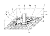
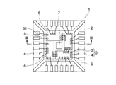
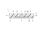
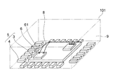
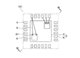
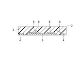
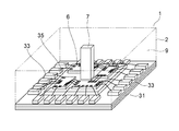
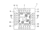
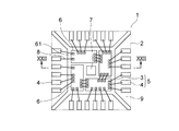
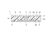
図1は、この発明の実施の形態1による半導体パッケージを示す斜視図である。また、図2は図1の半導体パッケージを示す上面図、図3は図2のIII−III線に沿った断面図である。本実施の形態では、QFN型の半導体パッケージについて説明する。半導体パッケージ1は、パッケージ本体2を有している。この例では、パッケージ本体2がそのまま半導体パッケージ1を構成している。パッケージ本体2は、ダイパッド3及び第1の端子である複数の信号用接続端子4を有するリードフレーム5と、ダイパッド3に設けられている半導体部品である2つ以上(この例では、4個)のICチップ6と、ダイパッド3に設けられている導電性部材である1つの導体柱7と、ICチップ6と複数の信号用接続端子4とを電気的に接続している複数のワイヤ8と、リードフレーム5、ICチップ6、導体柱7及び各ワイヤ8を封止している樹脂製のモールド部材9とを有している。
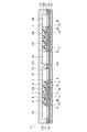
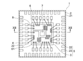
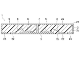
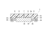
図12は、この発明の実施の形態2による半導体パッケージを示す上面図である。また、図13は、図12のXIII−XIII線に沿った断面図である。モールド部材9で封止されているリードフレーム5は、ダイパッド3と、第1の端子である複数の信号用接続端子22と、各信号用接続端子22と異なる第2の端子である複数の接地用接続端子23とを有している。ダイパッド3、各信号用接続端子22及び各接地用接続端子23は、互いに離れた状態で同一平面上に配置されている。複数の信号用接続端子22は、ダイパッド3の周囲に並べられている。複数の接地用接続端子23は、ダイパッド3及び各信号用接続端子22が配置された領域の周囲に並べられている。
実施の形態1及び2では、半導体パッケージ1にリードフレームが用いられているが、リードフレームの代わりにパッケージ用基板を半導体パッケージに用いてもよい。
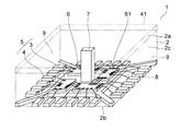
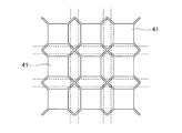
図20は、この発明の実施の形態4による半導体パッケージを示す斜視図である。また、図21は図20の半導体パッケージを示す上面図、図22は図21のXXII−XXII線に沿った断面図である。半導体パッケージ1は、実施の形態1と同様のパッケージ本体2と、パッケージ本体2の天面2aに重なっている導電性板41とを有している。
Claims (7)
- パッケージ本体を備え、
前記パッケージ本体は、
第1の端子及びダイパッドを有するリードフレームと、
前記ダイパッドに設けられている2つ以上のICチップと、
前記ダイパッドに設けられている1つ以上の導電性部材と、
前記第1の端子と前記ICチップとを電気的に接続しているワイヤと、
前記リードフレーム、前記ICチップ、前記導電性部材及び前記ワイヤを封止しているモールド部材と
を有し、
前記パッケージ本体の天面、底面及び側面は、前記モールド部材によって形成されており、
前記導電性部材は、前記パッケージ本体の天面から露出し、
前記ダイパッドは、前記パッケージ本体の底面から露出している半導体パッケージ。 - 前記パッケージ本体を覆っている導電性薄膜
を備え、
前記リードフレームは、前記第1の端子と異なる第2の端子をさらに有し、
前記第2の端子は、前記パッケージ本体の側面から露出し、
前記導電性薄膜は、前記パッケージ本体の天面及び側面を覆っている状態で、前記導電性部材及び前記第2の端子のそれぞれに電気的に接続されている請求項1に記載の半導体パッケージ。 - 前記パッケージ本体の天面に重なっている導電性板
を備え、
前記導電性板は、前記パッケージ本体の天面からの前記導電性部材の露出部分に接触し、
前記導電性板の形状は、前記ダイパッドの形状と同じである請求項1に記載の半導体パッケージ。 - パッケージ本体を備え、
前記パッケージ本体は、
端子パターンが設けられているパッケージ用基板と、
前記パッケージ用基板に設けられているメタルインレイと、
前記メタルインレイに設けられている2つ以上のICチップと、
前記メタルインレイに設けられている1つ以上の導電性部材と、
前記端子パターンと前記ICチップとを電気的に接続しているワイヤと、
前記ICチップ、前記導電性部材及び前記ワイヤを封止しているモールド部材と
を有し、
前記パッケージ本体の天面及び側面は、前記モールド部材によって形成され、
前記パッケージ本体の底面は、前記パッケージ用基板によって形成されており、
前記導電性部材は、前記パッケージ本体の天面から露出し、
前記メタルインレイは、前記パッケージ本体の底面から露出している半導体パッケージ。 - 前記パッケージ本体の天面に重なっている導電性板
を備え、
前記導電性板は、前記パッケージ本体の天面からの前記導電性部材の露出部分に接触している請求項1又は請求項4に記載の半導体パッケージ。 - 請求項1〜請求項5のいずれか一項に記載の半導体パッケージ、
接地導体が設けられ、前記半導体パッケージが実装されているモジュール用基板、及び
前記半導体パッケージを覆っている導電性のカバー
を備えているモジュールであって、
前記接地導体及び前記カバーは、互いに接続された状態で前記半導体パッケージを収容する遮蔽ケースを構成しており、
前記遮蔽ケースの内部に存在している前記導電性部材は、前記接地導体及び前記カバーのそれぞれに電気的に接続されているモジュール。 - 前記半導体パッケージと前記カバーとの間には、導電性充填材が介在しており、
前記導電性部材と前記カバーとは、前記導電性充填材を介して電気的に接続されている請求項6に記載のモジュール。
Applications Claiming Priority (1)
| Application Number | Priority Date | Filing Date | Title |
|---|---|---|---|
| PCT/JP2016/055658 WO2017145331A1 (ja) | 2016-02-25 | 2016-02-25 | 半導体パッケージ、及びモジュール |
Publications (2)
| Publication Number | Publication Date |
|---|---|
| JP6180646B1 JP6180646B1 (ja) | 2017-08-16 |
| JPWO2017145331A1 true JPWO2017145331A1 (ja) | 2018-03-01 |
Family
ID=59604985
Family Applications (1)
| Application Number | Title | Priority Date | Filing Date |
|---|---|---|---|
| JP2016544882A Active JP6180646B1 (ja) | 2016-02-25 | 2016-02-25 | 半導体パッケージ、及びモジュール |
Country Status (4)
| Country | Link |
|---|---|
| US (1) | US10964631B2 (ja) |
| EP (1) | EP3407378B1 (ja) |
| JP (1) | JP6180646B1 (ja) |
| WO (1) | WO2017145331A1 (ja) |
Families Citing this family (9)
| Publication number | Priority date | Publication date | Assignee | Title |
|---|---|---|---|---|
| WO2019051710A1 (zh) | 2017-09-14 | 2019-03-21 | 深圳市汇顶科技股份有限公司 | 芯片封装结构及方法、电子设备 |
| KR102525490B1 (ko) * | 2017-10-24 | 2023-04-24 | 삼성전자주식회사 | 인쇄 회로 기판, 반도체 패키지 및 반도체 패키지의 제조 방법 |
| WO2019124024A1 (ja) * | 2017-12-20 | 2019-06-27 | 三菱電機株式会社 | 半導体パッケージおよびその製造方法 |
| JP7144112B2 (ja) | 2018-09-19 | 2022-09-29 | ローム株式会社 | 半導体装置 |
| US12232247B2 (en) | 2020-05-07 | 2025-02-18 | Sumitomo Electric Industries, Ltd. | Circuit module and communication device |
| DE112020007228T5 (de) | 2020-05-22 | 2023-03-09 | Mitsubishi Electric Corporation | Halbleitervorrichtung und Verfahren zum Herstellen einer Halbleitervorrichtung |
| JP7331827B2 (ja) * | 2020-12-23 | 2023-08-23 | 株式会社デンソー | 半導体パッケージおよびこれを用いた電子装置 |
| EP4040483A3 (en) * | 2021-02-04 | 2022-10-26 | Murata Manufacturing Co., Ltd. | Electronic component with internal shielding |
| JP2023055205A (ja) * | 2021-10-05 | 2023-04-17 | 住友電工デバイス・イノベーション株式会社 | 半導体デバイス及び半導体デバイスの製造方法 |
Family Cites Families (23)
| Publication number | Priority date | Publication date | Assignee | Title |
|---|---|---|---|---|
| US5087961A (en) * | 1987-01-28 | 1992-02-11 | Lsi Logic Corporation | Semiconductor device package |
| JPH0472648U (ja) * | 1990-11-07 | 1992-06-26 | ||
| JPH0758245A (ja) * | 1993-08-12 | 1995-03-03 | Toshiba Corp | 半導体装置及びその製造方法 |
| JPH09172114A (ja) * | 1995-12-19 | 1997-06-30 | Nec Eng Ltd | 半導体フラットパッケージ |
| JPH10125830A (ja) * | 1996-10-24 | 1998-05-15 | Hitachi Ltd | 高周波モジュールおよびその製造方法 |
| NL1011929C2 (nl) * | 1999-04-29 | 2000-10-31 | 3P Licensing Bv | Werkwijze voor het inkapselen van elektronische componenten, in het bijzonder geintegreerde schakelingen. |
| JP2005252099A (ja) | 2004-03-05 | 2005-09-15 | Sharp Corp | 高周波用半導体装置 |
| US8053872B1 (en) * | 2007-06-25 | 2011-11-08 | Rf Micro Devices, Inc. | Integrated shield for a no-lead semiconductor device package |
| US7741158B2 (en) * | 2006-06-08 | 2010-06-22 | Unisem (Mauritius) Holdings Limited | Method of making thermally enhanced substrate-base package |
| JP2008258411A (ja) * | 2007-04-05 | 2008-10-23 | Rohm Co Ltd | 半導体装置および半導体装置の製造方法 |
| US7732917B2 (en) | 2007-10-02 | 2010-06-08 | Rohm Co., Ltd. | Power module |
| JP2009105389A (ja) * | 2007-10-02 | 2009-05-14 | Rohm Co Ltd | パワーモジュール |
| JP2009206204A (ja) * | 2008-02-26 | 2009-09-10 | Sharp Corp | 出力制御装置 |
| JP5155890B2 (ja) * | 2008-06-12 | 2013-03-06 | ルネサスエレクトロニクス株式会社 | 半導体装置およびその製造方法 |
| US8362598B2 (en) * | 2009-08-26 | 2013-01-29 | Amkor Technology Inc | Semiconductor device with electromagnetic interference shielding |
| JP2012019091A (ja) | 2010-07-08 | 2012-01-26 | Sony Corp | モジュールおよび携帯端末 |
| JP2012028484A (ja) * | 2010-07-22 | 2012-02-09 | Panasonic Corp | モジュールと、その製造方法 |
| WO2012011210A1 (ja) * | 2010-07-22 | 2012-01-26 | パナソニック株式会社 | 半導体装置及びその製造方法 |
| JP2013026296A (ja) * | 2011-07-19 | 2013-02-04 | Daikin Ind Ltd | パワーモジュール |
| JP6045427B2 (ja) * | 2013-04-08 | 2016-12-14 | 三菱電機株式会社 | 電磁波シールド構造および高周波モジュール構造 |
| JP6262776B2 (ja) | 2014-02-04 | 2018-01-17 | 太陽誘電株式会社 | 回路モジュール |
| JP6017492B2 (ja) | 2014-04-24 | 2016-11-02 | Towa株式会社 | 樹脂封止電子部品の製造方法、突起電極付き板状部材、及び樹脂封止電子部品 |
| EP3499560B1 (en) * | 2017-12-15 | 2021-08-18 | Infineon Technologies AG | Semiconductor module and method for producing the same |
-
2016
- 2016-02-25 WO PCT/JP2016/055658 patent/WO2017145331A1/ja not_active Ceased
- 2016-02-25 US US16/067,522 patent/US10964631B2/en active Active
- 2016-02-25 JP JP2016544882A patent/JP6180646B1/ja active Active
- 2016-02-25 EP EP16891488.5A patent/EP3407378B1/en active Active
Also Published As
| Publication number | Publication date |
|---|---|
| JP6180646B1 (ja) | 2017-08-16 |
| WO2017145331A1 (ja) | 2017-08-31 |
| US10964631B2 (en) | 2021-03-30 |
| US20200126896A1 (en) | 2020-04-23 |
| EP3407378B1 (en) | 2020-07-01 |
| EP3407378A1 (en) | 2018-11-28 |
| EP3407378A4 (en) | 2019-05-08 |
Similar Documents
| Publication | Publication Date | Title |
|---|---|---|
| JP6180646B1 (ja) | 半導体パッケージ、及びモジュール | |
| US10863656B2 (en) | Radio-frequency module | |
| US9177881B2 (en) | High-frequency semiconductor package and high-frequency semiconductor device | |
| US10667381B2 (en) | High frequency module | |
| US6057601A (en) | Heat spreader with a placement recess and bottom saw-teeth for connection to ground planes on a thin two-sided single-core BGA substrate | |
| US6972479B2 (en) | Package with stacked substrates | |
| JP5802695B2 (ja) | 半導体装置、半導体装置の製造方法 | |
| JP2008091714A (ja) | 半導体装置 | |
| CN103094238B (zh) | 引线框架和半导体器件 | |
| JP6239147B2 (ja) | 半導体パッケージ | |
| WO2020017582A1 (ja) | モジュール | |
| KR20110020548A (ko) | 반도체 패키지 및 그의 제조방법 | |
| JPWO2014188632A1 (ja) | 放熱構造を有する半導体装置および半導体装置の積層体 | |
| JP2018190882A (ja) | 半導体装置 | |
| JP2021082794A (ja) | 電子部品および電子装置 | |
| US6703700B2 (en) | Semiconductor packaging structure | |
| JP7091555B2 (ja) | 電力増幅装置 | |
| JP2018190875A (ja) | 半導体装置 | |
| CN103311231B (zh) | 半导体器件及其制造方法 | |
| JP6494723B2 (ja) | 半導体パッケージ | |
| JP6579396B2 (ja) | 半導体装置、及び基板 | |
| CN222705518U (zh) | 封装结构 | |
| US20240234355A1 (en) | Module | |
| TWI409927B (zh) | 具載體之封裝結構 | |
| KR20110030090A (ko) | 반도체 패키지 및 그 제조방법 |
Legal Events
| Date | Code | Title | Description |
|---|---|---|---|
| A521 | Request for written amendment filed |
Free format text: JAPANESE INTERMEDIATE CODE: A523 Effective date: 20160706 |
|
| A621 | Written request for application examination |
Free format text: JAPANESE INTERMEDIATE CODE: A621 Effective date: 20160706 |
|
| A871 | Explanation of circumstances concerning accelerated examination |
Free format text: JAPANESE INTERMEDIATE CODE: A871 Effective date: 20160706 |
|
| A521 | Request for written amendment filed |
Free format text: JAPANESE INTERMEDIATE CODE: A523 Effective date: 20160822 |
|
| A975 | Report on accelerated examination |
Free format text: JAPANESE INTERMEDIATE CODE: A971005 Effective date: 20160905 |
|
| A131 | Notification of reasons for refusal |
Free format text: JAPANESE INTERMEDIATE CODE: A131 Effective date: 20161108 |
|
| A521 | Request for written amendment filed |
Free format text: JAPANESE INTERMEDIATE CODE: A523 Effective date: 20170105 |
|
| A131 | Notification of reasons for refusal |
Free format text: JAPANESE INTERMEDIATE CODE: A131 Effective date: 20170404 |
|
| A521 | Request for written amendment filed |
Free format text: JAPANESE INTERMEDIATE CODE: A523 Effective date: 20170426 |
|
| TRDD | Decision of grant or rejection written | ||
| A01 | Written decision to grant a patent or to grant a registration (utility model) |
Free format text: JAPANESE INTERMEDIATE CODE: A01 Effective date: 20170620 |
|
| A61 | First payment of annual fees (during grant procedure) |
Free format text: JAPANESE INTERMEDIATE CODE: A61 Effective date: 20170718 |
|
| R150 | Certificate of patent or registration of utility model |
Ref document number: 6180646 Country of ref document: JP Free format text: JAPANESE INTERMEDIATE CODE: R150 |
|
| R250 | Receipt of annual fees |
Free format text: JAPANESE INTERMEDIATE CODE: R250 |
|
| R250 | Receipt of annual fees |
Free format text: JAPANESE INTERMEDIATE CODE: R250 |
|
| R250 | Receipt of annual fees |
Free format text: JAPANESE INTERMEDIATE CODE: R250 |
|
| R250 | Receipt of annual fees |
Free format text: JAPANESE INTERMEDIATE CODE: R250 |
|
| R250 | Receipt of annual fees |
Free format text: JAPANESE INTERMEDIATE CODE: R250 |
|
| R250 | Receipt of annual fees |
Free format text: JAPANESE INTERMEDIATE CODE: R250 |