KR100282003B1 - 칩 스케일 패키지 - Google Patents
칩 스케일 패키지Info
- Publication number
- KR100282003B1 KR100282003B1 KR1019970052814A KR19970052814A KR100282003B1 KR 100282003 B1 KR100282003 B1 KR 100282003B1 KR 1019970052814 A KR1019970052814 A KR 1019970052814A KR 19970052814 A KR19970052814 A KR 19970052814A KR 100282003 B1 KR100282003 B1 KR 100282003B1
- Authority
- KR
- South Korea
- Prior art keywords
- width
- scale package
- chip scale
- beam lead
- end portion
- Prior art date
- Legal status (The legal status is an assumption and is not a legal conclusion. Google has not performed a legal analysis and makes no representation as to the accuracy of the status listed.)
- Expired - Fee Related
Links
Images



Classifications
-
- H—ELECTRICITY
- H10—SEMICONDUCTOR DEVICES; ELECTRIC SOLID-STATE DEVICES NOT OTHERWISE PROVIDED FOR
- H10W—GENERIC PACKAGES, INTERCONNECTIONS, CONNECTORS OR OTHER CONSTRUCTIONAL DETAILS OF DEVICES COVERED BY CLASS H10
- H10W74/00—Encapsulations, e.g. protective coatings
- H10W74/10—Encapsulations, e.g. protective coatings characterised by their shape or disposition
- H10W74/111—Encapsulations, e.g. protective coatings characterised by their shape or disposition the semiconductor body being completely enclosed
- H10W74/129—Encapsulations, e.g. protective coatings characterised by their shape or disposition the semiconductor body being completely enclosed forming a chip-scale package [CSP]
-
- H—ELECTRICITY
- H10—SEMICONDUCTOR DEVICES; ELECTRIC SOLID-STATE DEVICES NOT OTHERWISE PROVIDED FOR
- H10W—GENERIC PACKAGES, INTERCONNECTIONS, CONNECTORS OR OTHER CONSTRUCTIONAL DETAILS OF DEVICES COVERED BY CLASS H10
- H10W70/00—Package substrates; Interposers; Redistribution layers [RDL]
- H10W70/60—Insulating or insulated package substrates; Interposers; Redistribution layers
- H10W70/67—Insulating or insulated package substrates; Interposers; Redistribution layers characterised by their insulating layers or insulating parts
- H10W70/688—Flexible insulating substrates
-
- H—ELECTRICITY
- H10—SEMICONDUCTOR DEVICES; ELECTRIC SOLID-STATE DEVICES NOT OTHERWISE PROVIDED FOR
- H10P—GENERIC PROCESSES OR APPARATUS FOR THE MANUFACTURE OR TREATMENT OF DEVICES COVERED BY CLASS H10
- H10P72/00—Handling or holding of wafers, substrates or devices during manufacture or treatment thereof
- H10P72/70—Handling or holding of wafers, substrates or devices during manufacture or treatment thereof for supporting or gripping
- H10P72/74—Handling or holding of wafers, substrates or devices during manufacture or treatment thereof for supporting or gripping using temporarily an auxiliary support
-
- H—ELECTRICITY
- H10—SEMICONDUCTOR DEVICES; ELECTRIC SOLID-STATE DEVICES NOT OTHERWISE PROVIDED FOR
- H10W—GENERIC PACKAGES, INTERCONNECTIONS, CONNECTORS OR OTHER CONSTRUCTIONAL DETAILS OF DEVICES COVERED BY CLASS H10
- H10W70/00—Package substrates; Interposers; Redistribution layers [RDL]
- H10W70/40—Leadframes
- H10W70/453—Leadframes comprising flexible metallic tapes
Landscapes
- Lead Frames For Integrated Circuits (AREA)
- Wire Bonding (AREA)
Abstract
Description
Claims (14)
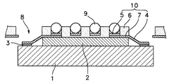
- 표면 에지부에 복수개의 본딩패드들이 형성된 반도체 칩과;상기 본딩패드가 노출되도록 상기 반도체 칩상에 절연 접착제를 개재하여 접착되고, 외부에 빔리드로 연장되는 도전패턴이 내부에 형성된 테이프와;상기 테이프의 도전패턴에 전기적으로 연결되는 솔더볼들을 포함하며,상기 빔리드는제 1 방향으로 형성된 전단부와;상기 제 1 방향에 대해 소정각도로 절곡된 제 2 방향으로 상기 전단부에서 연장된 제 1 연결부와;상기 제 1 방향으로 상기 제 1 연결부에서 연장된 접합부와;상기 제 2 방향으로 상기 접합부에서 연장된 제 2 연결부와;상기 제 1 방향으로 상기 제 2 연결부에 연장된 후단부로 이루어지고,상기 접합부는 상기 본딩패드에 전기적으로 연결되는 것을 특징으로 하는 칩 스케일 패키지.
- 제 1 항에 있어서, 상기 소정각도는 45도인 것을 특징으로 하는 칩 스케일 패키지.
- 제 1 항에 있어서, 상기 접합부의 폭은 상기 본딩패드의 폭의 40%∼70%의 크기를 갖는 것을 특징으로 하는 칩 스케일 패키지.
- 제 1 항에 있어서, 상기 전단부와 접합부 및 후단부는 각각의 폭을 길이방향으로 동일하게 유지하는 것을 특징으로 하는 칩 스케일 패키지.
- 제 1 항에 있어서, 상기 전단부의 폭은 상기 후단부의 폭의 2배인 것을 특징으로 하는 칩 스케일 패키지.
- 제 5 항에 있어서, 상기 전단부의 폭은 상기 접합부의 폭의 1.2배인 것을 특징으로 하는 칩 스케일 패키지.
- 제 1 항에 있어서, 상기 후단부의 폭은 5∼20㎛인 것을 특징으로 하는 칩 스케일 패키지.
- 제 1 항에 있어서, 상기 절연 접착제는 엘라스토머인 것을 특징으로 하는 칩 스케일 패키지.
- 제 8 항에 있어서, 상기 절연 접착제의 두께는 100㎛인 것을 특징으로 하는 칩 스케일 패키지.
- 제 1 항에 있어서, 상기 도전패턴은 구리박막이 베이스 필름상에 라미네이트되고 패터닝되어 형성되는 것을 특징으로 하는 칩 스케일 패키지.
- 제 10 항에 있어서, 상기 도전패턴은 금이나 주석 또는 이들의 합금으로 도금되는 것을 특징으로 하는 칩 스케일 패키지.
- 4면의 에지에 소정 폭으로 슬롯이 형성된 베이스 필름과;상기 베이스 필름상에 증착되어 소정형상으로 패터닝되고 상기 슬롯내에서 빔리드로 노출되는 도전패턴과;상기 도전패턴의 내측 단부에 형성된 솔더볼용 도전패드를 포함하며,상기 빔리드는제 1 방향으로 형성된 전단부와;상기 제 1 방향에 대해 소정각도로 절곡된 제 2 방향으로 상기 전단부에서 연장된 제 1 연결부와;상기 제 1 방향으로 상기 제 1 연결부에서 연장된 접합부와;상기 제 2 방향으로 상기 접합부에서 연장된 제 2 연결부와;상기 제 1 방향으로 상기 제 2 연결부에 연장된 후단부로 이루어지는 것을 특징으로 하는 칩 스케일 패키지용 테이프.
- 제 20 항에 있어서, 상기 소정 폭은 0.3㎜인 것을 특징으로 하는 칩 스케일 패키지용 테이프.
- 제 20 항에 있어서, 상기 소정각도는 45도인 것을 특징으로 하는 칩 스케일 패키지용 테이프.
Priority Applications (4)
| Application Number | Priority Date | Filing Date | Title |
|---|---|---|---|
| KR1019970052814A KR100282003B1 (ko) | 1997-10-15 | 1997-10-15 | 칩 스케일 패키지 |
| TW087104490A TW428255B (en) | 1997-10-15 | 1998-03-25 | Chip scale package |
| JP08892998A JP3663295B2 (ja) | 1997-10-15 | 1998-04-01 | チップスケールパッケージ |
| US09/154,665 US6037662A (en) | 1997-10-15 | 1998-09-18 | Chip scale package |
Applications Claiming Priority (1)
| Application Number | Priority Date | Filing Date | Title |
|---|---|---|---|
| KR1019970052814A KR100282003B1 (ko) | 1997-10-15 | 1997-10-15 | 칩 스케일 패키지 |
Publications (2)
| Publication Number | Publication Date |
|---|---|
| KR19990031914A KR19990031914A (ko) | 1999-05-06 |
| KR100282003B1 true KR100282003B1 (ko) | 2001-02-15 |
Family
ID=19522775
Family Applications (1)
| Application Number | Title | Priority Date | Filing Date |
|---|---|---|---|
| KR1019970052814A Expired - Fee Related KR100282003B1 (ko) | 1997-10-15 | 1997-10-15 | 칩 스케일 패키지 |
Country Status (4)
| Country | Link |
|---|---|
| US (1) | US6037662A (ko) |
| JP (1) | JP3663295B2 (ko) |
| KR (1) | KR100282003B1 (ko) |
| TW (1) | TW428255B (ko) |
Cited By (1)
| Publication number | Priority date | Publication date | Assignee | Title |
|---|---|---|---|---|
| US7598617B2 (en) | 2006-03-17 | 2009-10-06 | Hynix Semiconductor Inc. | Stack package utilizing through vias and re-distribution lines |
Families Citing this family (15)
| Publication number | Priority date | Publication date | Assignee | Title |
|---|---|---|---|---|
| KR100604332B1 (ko) * | 1999-02-11 | 2006-07-24 | 삼성테크윈 주식회사 | 반도체 패키지 및 그 제조방법 |
| US6143581A (en) * | 1999-02-22 | 2000-11-07 | Micron Technology, Inc. | Asymmetric transfer molding method and an asymmetric encapsulation made therefrom |
| US6537853B1 (en) | 1999-02-22 | 2003-03-25 | Micron Technology, Inc. | Overmolding encapsulation process |
| US6362429B1 (en) * | 1999-08-18 | 2002-03-26 | Micron Technology, Inc. | Stress relieving tape bonding interconnect |
| TW478089B (en) * | 1999-10-29 | 2002-03-01 | Hitachi Ltd | Semiconductor device and the manufacturing method thereof |
| TW498468B (en) | 1999-10-29 | 2002-08-11 | Hitachi Ltd | Semiconductor device |
| US6770547B1 (en) | 1999-10-29 | 2004-08-03 | Renesas Technology Corporation | Method for producing a semiconductor device |
| US6696765B2 (en) * | 2001-11-19 | 2004-02-24 | Hitachi, Ltd. | Multi-chip module |
| KR100549409B1 (ko) * | 2003-03-11 | 2006-02-08 | 삼성전자주식회사 | 파상의 빔 리드를 구비하는 테이프 배선 기판 및 그를이용한 반도체 칩 패키지 |
| JP4393303B2 (ja) * | 2003-09-05 | 2010-01-06 | キヤノン株式会社 | 半導体装置の製造方法 |
| KR101358751B1 (ko) * | 2007-10-16 | 2014-02-07 | 삼성전자주식회사 | 반도체 패키지 |
| IT1402273B1 (it) * | 2010-07-29 | 2013-08-28 | St Microelectronics Srl | Elemento a semiconduttore con un die semiconduttore e telai di connettori |
| DE102014105861B4 (de) * | 2014-04-25 | 2015-11-05 | Infineon Technologies Ag | Sensorvorrichtung und Verfahren zum Herstellen einer Sensorvorrichtung |
| JP6513465B2 (ja) | 2015-04-24 | 2019-05-15 | 日本航空電子工業株式会社 | リード接合構造 |
| US10607928B1 (en) | 2019-04-08 | 2020-03-31 | International Business Machines Corporation | Reduction of laminate failure in integrated circuit (IC) device carrier |
Citations (2)
| Publication number | Priority date | Publication date | Assignee | Title |
|---|---|---|---|---|
| JPS6163047A (ja) * | 1985-06-28 | 1986-04-01 | Hitachi Ltd | 樹脂封止型形半導体装置用リ−ドフレ−ム |
| JPH09260535A (ja) * | 1996-03-22 | 1997-10-03 | Hitachi Ltd | 半導体集積回路装置およびその製造方法 |
Family Cites Families (4)
| Publication number | Priority date | Publication date | Assignee | Title |
|---|---|---|---|---|
| FR2299724A1 (fr) * | 1975-01-29 | 1976-08-27 | Honeywell Bull Soc Ind | Perfectionnements aux supports de conditionnement de micro-plaquettes de circuits integres |
| US5148265A (en) * | 1990-09-24 | 1992-09-15 | Ist Associates, Inc. | Semiconductor chip assemblies with fan-in leads |
| JPH08316270A (ja) * | 1995-05-23 | 1996-11-29 | Hitachi Ltd | テープキャリアおよびそれを用いた半導体装置 |
| US5866949A (en) * | 1996-12-02 | 1999-02-02 | Minnesota Mining And Manufacturing Company | Chip scale ball grid array for integrated circuit packaging |
-
1997
- 1997-10-15 KR KR1019970052814A patent/KR100282003B1/ko not_active Expired - Fee Related
-
1998
- 1998-03-25 TW TW087104490A patent/TW428255B/zh not_active IP Right Cessation
- 1998-04-01 JP JP08892998A patent/JP3663295B2/ja not_active Expired - Fee Related
- 1998-09-18 US US09/154,665 patent/US6037662A/en not_active Expired - Lifetime
Patent Citations (2)
| Publication number | Priority date | Publication date | Assignee | Title |
|---|---|---|---|---|
| JPS6163047A (ja) * | 1985-06-28 | 1986-04-01 | Hitachi Ltd | 樹脂封止型形半導体装置用リ−ドフレ−ム |
| JPH09260535A (ja) * | 1996-03-22 | 1997-10-03 | Hitachi Ltd | 半導体集積回路装置およびその製造方法 |
Cited By (1)
| Publication number | Priority date | Publication date | Assignee | Title |
|---|---|---|---|---|
| US7598617B2 (en) | 2006-03-17 | 2009-10-06 | Hynix Semiconductor Inc. | Stack package utilizing through vias and re-distribution lines |
Also Published As
| Publication number | Publication date |
|---|---|
| JP3663295B2 (ja) | 2005-06-22 |
| JPH11121543A (ja) | 1999-04-30 |
| US6037662A (en) | 2000-03-14 |
| TW428255B (en) | 2001-04-01 |
| KR19990031914A (ko) | 1999-05-06 |
Similar Documents
| Publication | Publication Date | Title |
|---|---|---|
| US6861734B2 (en) | Resin-molded semiconductor device | |
| US20010007285A1 (en) | Resin sealed semiconductor device, circuit member for use therein and method of manufacturing circuit member | |
| KR20030051222A (ko) | 반도체 장치 및 그 제조 방법 | |
| US5895234A (en) | Semiconductor device and method for producing the same | |
| KR19990031914A (ko) | 칩 스케일 패키지 | |
| JPWO1998018161A1 (ja) | 半導体装置及びその製造方法、回路基板並びにフィルムキャリアテープ | |
| US20020017706A1 (en) | Lead frame, semiconductor device and manufacturing method therefor, circuit board and electronic equipment | |
| US6962836B2 (en) | Method of manufacturing a semiconductor device having leads stabilized during die mounting | |
| JP2000307049A (ja) | リードフレームとそれを用いた樹脂封止型半導体装置およびその製造方法 | |
| KR100292033B1 (ko) | 반도체칩패키지및그제조방법 | |
| US5406119A (en) | Lead frame | |
| JP3008470B2 (ja) | リードフレーム | |
| JP3427492B2 (ja) | 凸型ヒートシンク付き半導体装置及びその凸型ヒートシンクの製造方法 | |
| JP2001024133A (ja) | リードフレームとそれを用いた樹脂封止型半導体装置およびその製造方法 | |
| JP3029736B2 (ja) | 混成集積回路装置の製造方法 | |
| JPH11297917A (ja) | 半導体装置及びその製造方法 | |
| JPH0936275A (ja) | 表面実装型半導体装置の製造方法 | |
| JPH06252334A (ja) | 半導体装置 | |
| JPH11176849A (ja) | 半導体装置の製造方法 | |
| JPH06236956A (ja) | 半導体装置及びその製造方法 | |
| JP2001077275A (ja) | リードフレームとそれを用いた樹脂封止型半導体装置の製造方法 | |
| JP2001077285A (ja) | リードフレームとそれを用いた樹脂封止型半導体装置の製造方法 | |
| KR200159861Y1 (ko) | 반도체 패키지 | |
| JP2726648B2 (ja) | 半導体装置 | |
| KR20030025481A (ko) | 플립칩 반도체패키지 및 그의 제조방법 |
Legal Events
| Date | Code | Title | Description |
|---|---|---|---|
| A201 | Request for examination | ||
| PA0109 | Patent application |
St.27 status event code: A-0-1-A10-A12-nap-PA0109 |
|
| PA0201 | Request for examination |
St.27 status event code: A-1-2-D10-D11-exm-PA0201 |
|
| R17-X000 | Change to representative recorded |
St.27 status event code: A-3-3-R10-R17-oth-X000 |
|
| R18-X000 | Changes to party contact information recorded |
St.27 status event code: A-3-3-R10-R18-oth-X000 |
|
| PN2301 | Change of applicant |
St.27 status event code: A-3-3-R10-R13-asn-PN2301 St.27 status event code: A-3-3-R10-R11-asn-PN2301 |
|
| PG1501 | Laying open of application |
St.27 status event code: A-1-1-Q10-Q12-nap-PG1501 |
|
| E902 | Notification of reason for refusal | ||
| PE0902 | Notice of grounds for rejection |
St.27 status event code: A-1-2-D10-D21-exm-PE0902 |
|
| AMND | Amendment | ||
| P11-X000 | Amendment of application requested |
St.27 status event code: A-2-2-P10-P11-nap-X000 |
|
| P13-X000 | Application amended |
St.27 status event code: A-2-2-P10-P13-nap-X000 |
|
| PN2301 | Change of applicant |
St.27 status event code: A-3-3-R10-R13-asn-PN2301 St.27 status event code: A-3-3-R10-R11-asn-PN2301 |
|
| E601 | Decision to refuse application | ||
| PE0601 | Decision on rejection of patent |
St.27 status event code: N-2-6-B10-B15-exm-PE0601 |
|
| AMND | Amendment | ||
| J201 | Request for trial against refusal decision | ||
| P11-X000 | Amendment of application requested |
St.27 status event code: A-2-2-P10-P11-nap-X000 |
|
| P13-X000 | Application amended |
St.27 status event code: A-2-2-P10-P13-nap-X000 |
|
| PJ0201 | Trial against decision of rejection |
St.27 status event code: A-3-3-V10-V11-apl-PJ0201 |
|
| PB0901 | Examination by re-examination before a trial |
St.27 status event code: A-6-3-E10-E12-rex-PB0901 |
|
| B601 | Maintenance of original decision after re-examination before a trial | ||
| PB0601 | Maintenance of original decision after re-examination before a trial |
St.27 status event code: N-3-6-B10-B17-rex-PB0601 |
|
| R18-X000 | Changes to party contact information recorded |
St.27 status event code: A-3-3-R10-R18-oth-X000 |
|
| J301 | Trial decision |
Free format text: TRIAL DECISION FOR APPEAL AGAINST DECISION TO DECLINE REFUSAL REQUESTED 19991221 Effective date: 20000831 |
|
| PJ1301 | Trial decision |
St.27 status event code: A-3-3-V10-V15-crt-PJ1301 Decision date: 20000831 Appeal event data comment text: Appeal Kind Category : Appeal against decision to decline refusal, Appeal Ground Text : 1997 52814 Appeal request date: 19991221 Appellate body name: Patent Examination Board Decision authority category: Office appeal board Decision identifier: 1999101004594 |
|
| PS0901 | Examination by remand of revocation |
St.27 status event code: A-6-3-E10-E12-rex-PS0901 |
|
| S901 | Examination by remand of revocation | ||
| GRNO | Decision to grant (after opposition) | ||
| PS0701 | Decision of registration after remand of revocation |
St.27 status event code: A-3-4-F10-F13-rex-PS0701 |
|
| GRNT | Written decision to grant | ||
| PR0701 | Registration of establishment |
St.27 status event code: A-2-4-F10-F11-exm-PR0701 |
|
| PR1002 | Payment of registration fee |
St.27 status event code: A-2-2-U10-U11-oth-PR1002 Fee payment year number: 1 |
|
| PG1601 | Publication of registration |
St.27 status event code: A-4-4-Q10-Q13-nap-PG1601 |
|
| PN2301 | Change of applicant |
St.27 status event code: A-5-5-R10-R13-asn-PN2301 St.27 status event code: A-5-5-R10-R11-asn-PN2301 |
|
| R18-X000 | Changes to party contact information recorded |
St.27 status event code: A-5-5-R10-R18-oth-X000 |
|
| R18-X000 | Changes to party contact information recorded |
St.27 status event code: A-5-5-R10-R18-oth-X000 |
|
| PR1001 | Payment of annual fee |
St.27 status event code: A-4-4-U10-U11-oth-PR1001 Fee payment year number: 4 |
|
| R18-X000 | Changes to party contact information recorded |
St.27 status event code: A-5-5-R10-R18-oth-X000 |
|
| PR1001 | Payment of annual fee |
St.27 status event code: A-4-4-U10-U11-oth-PR1001 Fee payment year number: 5 |
|
| PN2301 | Change of applicant |
St.27 status event code: A-5-5-R10-R13-asn-PN2301 St.27 status event code: A-5-5-R10-R11-asn-PN2301 |
|
| PN2301 | Change of applicant |
St.27 status event code: A-5-5-R10-R13-asn-PN2301 St.27 status event code: A-5-5-R10-R11-asn-PN2301 |
|
| PR1001 | Payment of annual fee |
St.27 status event code: A-4-4-U10-U11-oth-PR1001 Fee payment year number: 6 |
|
| PR1001 | Payment of annual fee |
St.27 status event code: A-4-4-U10-U11-oth-PR1001 Fee payment year number: 7 |
|
| FPAY | Annual fee payment |
Payment date: 20071101 Year of fee payment: 8 |
|
| PR1001 | Payment of annual fee |
St.27 status event code: A-4-4-U10-U11-oth-PR1001 Fee payment year number: 8 |
|
| LAPS | Lapse due to unpaid annual fee | ||
| PC1903 | Unpaid annual fee |
St.27 status event code: A-4-4-U10-U13-oth-PC1903 Not in force date: 20081124 Payment event data comment text: Termination Category : DEFAULT_OF_REGISTRATION_FEE |
|
| PC1903 | Unpaid annual fee |
St.27 status event code: N-4-6-H10-H13-oth-PC1903 Ip right cessation event data comment text: Termination Category : DEFAULT_OF_REGISTRATION_FEE Not in force date: 20081124 |
|
| R18-X000 | Changes to party contact information recorded |
St.27 status event code: A-5-5-R10-R18-oth-X000 |
|
| P22-X000 | Classification modified |
St.27 status event code: A-4-4-P10-P22-nap-X000 |
|
| P22-X000 | Classification modified |
St.27 status event code: A-4-4-P10-P22-nap-X000 |