KR20120065249A - 표시 장치, 및 그 제작 방법 - Google Patents
표시 장치, 및 그 제작 방법 Download PDFInfo
- Publication number
- KR20120065249A KR20120065249A KR1020110130968A KR20110130968A KR20120065249A KR 20120065249 A KR20120065249 A KR 20120065249A KR 1020110130968 A KR1020110130968 A KR 1020110130968A KR 20110130968 A KR20110130968 A KR 20110130968A KR 20120065249 A KR20120065249 A KR 20120065249A
- Authority
- KR
- South Korea
- Prior art keywords
- layer
- insulating layer
- electrode
- semiconductor layer
- semiconductor
- Prior art date
- Legal status (The legal status is an assumption and is not a legal conclusion. Google has not performed a legal analysis and makes no representation as to the accuracy of the status listed.)
- Ceased
Links
Images


Classifications
-
- G—PHYSICS
- G02—OPTICS
- G02F—OPTICAL DEVICES OR ARRANGEMENTS FOR THE CONTROL OF LIGHT BY MODIFICATION OF THE OPTICAL PROPERTIES OF THE MEDIA OF THE ELEMENTS INVOLVED THEREIN; NON-LINEAR OPTICS; FREQUENCY-CHANGING OF LIGHT; OPTICAL LOGIC ELEMENTS; OPTICAL ANALOGUE/DIGITAL CONVERTERS
- G02F1/00—Devices or arrangements for the control of the intensity, colour, phase, polarisation or direction of light arriving from an independent light source, e.g. switching, gating or modulating; Non-linear optics
- G02F1/01—Devices or arrangements for the control of the intensity, colour, phase, polarisation or direction of light arriving from an independent light source, e.g. switching, gating or modulating; Non-linear optics for the control of the intensity, phase, polarisation or colour
- G02F1/13—Devices or arrangements for the control of the intensity, colour, phase, polarisation or direction of light arriving from an independent light source, e.g. switching, gating or modulating; Non-linear optics for the control of the intensity, phase, polarisation or colour based on liquid crystals, e.g. single liquid crystal display cells
- G02F1/133—Constructional arrangements; Operation of liquid crystal cells; Circuit arrangements
- G02F1/136—Liquid crystal cells structurally associated with a semi-conducting layer or substrate, e.g. cells forming part of an integrated circuit
- G02F1/1362—Active matrix addressed cells
- G02F1/1368—Active matrix addressed cells in which the switching element is a three-electrode device
-
- H—ELECTRICITY
- H10—SEMICONDUCTOR DEVICES; ELECTRIC SOLID-STATE DEVICES NOT OTHERWISE PROVIDED FOR
- H10D—INORGANIC ELECTRIC SEMICONDUCTOR DEVICES
- H10D30/00—Field-effect transistors [FET]
- H10D30/60—Insulated-gate field-effect transistors [IGFET]
- H10D30/67—Thin-film transistors [TFT]
- H10D30/6704—Thin-film transistors [TFT] having supplementary regions or layers in the thin films or in the insulated bulk substrates for controlling properties of the device
-
- H—ELECTRICITY
- H10—SEMICONDUCTOR DEVICES; ELECTRIC SOLID-STATE DEVICES NOT OTHERWISE PROVIDED FOR
- H10D—INORGANIC ELECTRIC SEMICONDUCTOR DEVICES
- H10D30/00—Field-effect transistors [FET]
- H10D30/60—Insulated-gate field-effect transistors [IGFET]
- H10D30/67—Thin-film transistors [TFT]
- H10D30/6729—Thin-film transistors [TFT] characterised by the electrodes
- H10D30/673—Thin-film transistors [TFT] characterised by the electrodes characterised by the shapes, relative sizes or dispositions of the gate electrodes
-
- H—ELECTRICITY
- H10—SEMICONDUCTOR DEVICES; ELECTRIC SOLID-STATE DEVICES NOT OTHERWISE PROVIDED FOR
- H10D—INORGANIC ELECTRIC SEMICONDUCTOR DEVICES
- H10D86/00—Integrated devices formed in or on insulating or conducting substrates, e.g. formed in silicon-on-insulator [SOI] substrates or on stainless steel or glass substrates
- H10D86/01—Manufacture or treatment
- H10D86/021—Manufacture or treatment of multiple TFTs
- H10D86/0231—Manufacture or treatment of multiple TFTs using masks, e.g. half-tone masks
-
- H—ELECTRICITY
- H10—SEMICONDUCTOR DEVICES; ELECTRIC SOLID-STATE DEVICES NOT OTHERWISE PROVIDED FOR
- H10D—INORGANIC ELECTRIC SEMICONDUCTOR DEVICES
- H10D86/00—Integrated devices formed in or on insulating or conducting substrates, e.g. formed in silicon-on-insulator [SOI] substrates or on stainless steel or glass substrates
- H10D86/40—Integrated devices formed in or on insulating or conducting substrates, e.g. formed in silicon-on-insulator [SOI] substrates or on stainless steel or glass substrates characterised by multiple TFTs
- H10D86/421—Integrated devices formed in or on insulating or conducting substrates, e.g. formed in silicon-on-insulator [SOI] substrates or on stainless steel or glass substrates characterised by multiple TFTs having a particular composition, shape or crystalline structure of the active layer
- H10D86/423—Integrated devices formed in or on insulating or conducting substrates, e.g. formed in silicon-on-insulator [SOI] substrates or on stainless steel or glass substrates characterised by multiple TFTs having a particular composition, shape or crystalline structure of the active layer comprising semiconductor materials not belonging to the Group IV, e.g. InGaZnO
-
- H—ELECTRICITY
- H10—SEMICONDUCTOR DEVICES; ELECTRIC SOLID-STATE DEVICES NOT OTHERWISE PROVIDED FOR
- H10D—INORGANIC ELECTRIC SEMICONDUCTOR DEVICES
- H10D86/00—Integrated devices formed in or on insulating or conducting substrates, e.g. formed in silicon-on-insulator [SOI] substrates or on stainless steel or glass substrates
- H10D86/40—Integrated devices formed in or on insulating or conducting substrates, e.g. formed in silicon-on-insulator [SOI] substrates or on stainless steel or glass substrates characterised by multiple TFTs
- H10D86/451—Integrated devices formed in or on insulating or conducting substrates, e.g. formed in silicon-on-insulator [SOI] substrates or on stainless steel or glass substrates characterised by multiple TFTs characterised by the compositions or shapes of the interlayer dielectrics
-
- H—ELECTRICITY
- H10—SEMICONDUCTOR DEVICES; ELECTRIC SOLID-STATE DEVICES NOT OTHERWISE PROVIDED FOR
- H10D—INORGANIC ELECTRIC SEMICONDUCTOR DEVICES
- H10D86/00—Integrated devices formed in or on insulating or conducting substrates, e.g. formed in silicon-on-insulator [SOI] substrates or on stainless steel or glass substrates
- H10D86/40—Integrated devices formed in or on insulating or conducting substrates, e.g. formed in silicon-on-insulator [SOI] substrates or on stainless steel or glass substrates characterised by multiple TFTs
- H10D86/481—Integrated devices formed in or on insulating or conducting substrates, e.g. formed in silicon-on-insulator [SOI] substrates or on stainless steel or glass substrates characterised by multiple TFTs integrated with passive devices, e.g. auxiliary capacitors
-
- H—ELECTRICITY
- H10—SEMICONDUCTOR DEVICES; ELECTRIC SOLID-STATE DEVICES NOT OTHERWISE PROVIDED FOR
- H10D—INORGANIC ELECTRIC SEMICONDUCTOR DEVICES
- H10D86/00—Integrated devices formed in or on insulating or conducting substrates, e.g. formed in silicon-on-insulator [SOI] substrates or on stainless steel or glass substrates
- H10D86/40—Integrated devices formed in or on insulating or conducting substrates, e.g. formed in silicon-on-insulator [SOI] substrates or on stainless steel or glass substrates characterised by multiple TFTs
- H10D86/60—Integrated devices formed in or on insulating or conducting substrates, e.g. formed in silicon-on-insulator [SOI] substrates or on stainless steel or glass substrates characterised by multiple TFTs wherein the TFTs are in active matrices
-
- H—ELECTRICITY
- H10—SEMICONDUCTOR DEVICES; ELECTRIC SOLID-STATE DEVICES NOT OTHERWISE PROVIDED FOR
- H10D—INORGANIC ELECTRIC SEMICONDUCTOR DEVICES
- H10D30/00—Field-effect transistors [FET]
- H10D30/60—Insulated-gate field-effect transistors [IGFET]
- H10D30/67—Thin-film transistors [TFT]
- H10D30/6729—Thin-film transistors [TFT] characterised by the electrodes
Landscapes
- Physics & Mathematics (AREA)
- Nonlinear Science (AREA)
- Mathematical Physics (AREA)
- Engineering & Computer Science (AREA)
- Chemical & Material Sciences (AREA)
- Crystallography & Structural Chemistry (AREA)
- Microelectronics & Electronic Packaging (AREA)
- General Physics & Mathematics (AREA)
- Optics & Photonics (AREA)
- Thin Film Transistor (AREA)
- Liquid Crystal (AREA)
- Electroluminescent Light Sources (AREA)
- Devices For Indicating Variable Information By Combining Individual Elements (AREA)
Abstract
Description
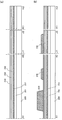
도 2는 본 발명의 일 형태를 설명하는 상면도 및 단면도.
도 3은 본 발명의 일 형태를 설명하는 상면도 및 단면도.
도 4는 본 발명의 일 형태를 설명하는 회로도.
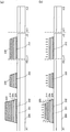
도 5는 본 발명의 일 형태를 설명하는 상면도 및 단면도.
도 6은 본 발명의 일 형태를 설명하는 단면도.
도 7은 본 발명의 일 형태를 설명하는 단면도.
도 8은 본 발명의 일 형태를 설명하는 단면도.
도 9는 본 발명의 일 형태를 설명하는 단면도.
도 10은 본 발명의 일 형태를 설명하는 단면도.
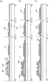
도 11은 본 발명의 일 형태를 설명하는 도면.
도 12는 전자 기기의 일례를 설명하는 도면.
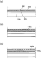
도 13은 다계조 마스크의 일례를 설명하는 도면.
102 화소 영역 103 단자부
104 단자부 105 단자
106 단자 107 단자
110 화소 111 트랜지스터
112 액정 소자 113 용량 소자
114 전극 120 화소
123 용량 소자 130 화소
133 용량 소자 200 기판
201 절연층 202 게이트 전극
203 배선 204 절연층
205 반도체층 208 콘택트 홀
210 화소 전극 212 배선
214 절연층 215 절연층
216 배선 219 콘택트 홀
221 전극 222 전극
223 전극 231 도전층
232 절연층 233 반도체층
234 절연층 235 레지스트 마스크
802 투광성 기판 803 차광부
804 회절 격자 805 광투과율
806 차광부 807 반투과부
808 광투과율 2702 케이스
2704 케이스 2705 표시부
2707 표시부 2712 축부
2721 전원 단자 2723 조작 키
2725 스피커 2800 케이스
2801 케이스 2802 표시 패널
2803 스피커 2804 마이크로폰
2805 조작 키 2806 포인팅 디바이스
2807 카메라용 렌즈 2808 외부 접속 단자
2810 태양 전지 셀 2811 외부 메모리 슬롯
3001 본체 3002 케이스
3003 표시부 3004 키보드
3021 본체 3022 스타일러스
3023 표시부 3024 조작 버튼
3025 외부 인터페이스 3051 본체
3053 접안부 3054 조작 스위치
3055 표시부(B) 3056 배터리
3057 표시부(A) 4001 기판
4002 화소부 4003 신호선 구동 회로
4004 주사선 구동 회로 4005 씰재
4006 기판 4008 액정층
4010 트랜지스터 4011 용량 소자
4013 액정 소자 4015 전극
4016 배선 4018 FPC
4019 이방성 도전층 4020 입력 단자
4030 전극 4031 전극
4032 절연층 4033 절연층
4035 스페이서 9601 케이스
9603 표시부 9605 스탠드
148a 결정성 산화물 반도체층 148b 결정성 산화물 반도체층
206a 소스 전극 206b 드레인 전극
4018a FPC 4018b FPC
801a 그레이톤 마스크 801b 하프톤 마스크
Claims (20)
- 게이트 전극;
게이트 절연층;
반도체층;
채널 보호층;
소스 전극; 및
드레인 전극을 포함하고,
상기 소스 전극 및 상기 드레인 전극은 상기 채널 보호층의 콘택트 홀들을 통해 상기 반도체층에 전기적으로 접속되고,
상기 드레인 전극은 화소 전극에 전기적으로 접속되고,
일 측면 상의 상기 게이트 절연층, 상기 반도체층, 및 상기 채널 보호층의 측면들은 대체로 서로 나란히 정렬되는, 표시 장치. - 제 1 항에 있어서,
상기 게이트 전극은 상기 반도체층과 중첩하고,
상기 게이트 전극의 단부는 상기 반도체층의 단부 외측으로 돌출되는, 표시 장치. - 제 1 항에 있어서,
상기 반도체층은 산화물 반도체층인, 표시 장치. - 제 1 항에 있어서,
상기 게이트 전극, 상기 소스 전극, 또는 상기 드레인 전극은 구리를 함유하는 재료를 포함하는, 표시 장치. - 제 1 항에 있어서,
상기 게이트 전극 아래에 기저층이 형성되는, 표시 장치. - 트랜지스터; 및
용량 소자를 포함하는, 표시 장치로서,
상기 트랜지스터는,
게이트 전극 위에 형성된 게이트 절연층;
상기 게이트 절연층 위에 형성된 반도체층;
상기 반도체층 위에 형성된 제 1 채널 보호층;
상기 제 1 채널 보호층 위에 형성된 제 2 채널 보호층; 및
상기 제 2 채널 보호층 위에 형성되고, 상기 제 1 채널 보호층 및 상기 제 2 채널 보호층의 콘택트 홀을 통하여 상기 반도체층에 전기적으로 접속되는 소스 전극 및 드레인 전극을 포함하고,
상기 드레인 전극은 화소 전극에 전기적으로 접속되고,
일 측면 상의 상기 트랜지스터의 상기 게이트 절연층, 상기 반도체층, 및 상기 제 1 채널 보호층의 측면들은 대체로 서로 나란히 정렬되고,
상기 용량 소자는 용량 배선, 상기 드레인 전극, 및 상기 용량 배선과 상기 드레인 전극 사이에 개재된 상기 제 2 채널 보호층을 포함하는, 표시 장치. - 제 6 항에 있어서,
상기 게이트 전극은 상기 반도체층과 중첩하고,
상기 게이트 전극의 단부는 상기 반도체층의 단부 외측으로 돌출되는, 표시 장치. - 제 6 항에 있어서,
상기 반도체층은 산화물 반도체층인, 표시 장치. - 제 6 항에 있어서,
상기 게이트 전극, 상기 소스 전극, 또는 상기 드레인 전극은 구리를 함유하는 재료를 포함하는, 표시 장치. - 제 6 항에 있어서,
상기 게이트 전극 아래에 기저층이 형성되는, 표시 장치. - 도전층, 제 1 절연층, 반도체층, 및 제 2 절연층을 형성하는 단계;
제 1 포토리소그래피 공정을 통해 상기 도전층, 상기 제 1 절연층, 상기 반도체층, 및 상기 제 2 절연층을 선택적으로 제거함으로써 게이트 전극 및 섬 형상 반도체층을 형성하는 단계;
제 2 포토리소그래피 공정을 통해 상기 제 2 절연층의 일부를 선택적으로 제거함으로써 상기 섬 형상 반도체층의 일부를 노출하는 단계;
제 3 포토리소그래피 공정을 통해 소스 전극 및 드레인 전극을 형성하는 단계; 및
제 4 포토리소그래피 공정을 통해 화소 전극을 형성하는 단계를 포함하는, 표시 장치 제작 방법. - 제 11 항에 있어서,
상기 도전층, 상기 제 1 절연층, 상기 반도체층, 및 상기 제 2 절연층은 대기에 노출되지 않고 형성되는, 표시 장치 제작 방법. - 제 11 항에 있어서,
산화물 반도체가 상기 반도체층으로 사용되는, 표시 장치 제작 방법. - 제 11 항에 있어서,
상기 게이트 전극, 상기 소스 전극, 및 상기 드레인 전극은 구리를 함유하는 재료를 포함하는, 표시 장치 제작 방법. - 제 11 항에 있어서,
상기 게이트 전극, 상기 소스 전극, 또는 상기 드레인 전극이 형성된 후의 최고 프로세스 온도는 450℃ 이하인, 표시 장치 제작 방법. - 도전층, 제 1 절연층, 반도체층, 및 제 2 절연층을 형성하는 단계;
제 1 포토리소그래피 공정을 통해 상기 도전층, 상기 제 1 절연층, 상기 반도체층, 및 상기 제 2 절연층을 선택적으로 제거함으로써 게이트 전극, 용량 배선, 및 섬 형상 반도체층을 형성하는 단계;
상기 게이트 전극, 상기 용량 배선, 및 상기 섬 형상 반도체층을 덮는 제 3 절연층을 형성하는 단계;
제 2 포토리소그래피 공정을 통해 상기 제 2 절연층 및 상기 제 3 절연층의 일부를 선택적으로 제거함으로써 상기 섬 형상 반도체층의 일부를 노출하는 단계;
제 3 포토리소그래피 공정을 통해 소스 전극 및 드레인 전극을 형성하는 단계; 및
제 4 포토리소그래피 공정을 통해 화소 전극을 형성하는 단계를 포함하고,
상기 드레인 전극의 일부는 상기 제 3 절연층 및 상기 용량 배선과 중첩하는, 표시 장치 제작 방법. - 제 16 항에 있어서,
상기 도전층, 상기 제 1 절연층, 상기 반도체층, 및 상기 제 2 절연층은 대기에 노출되지 않고 형성되는, 표시 장치 제작 방법. - 제 16 항에 있어서,
산화물 반도체가 상기 반도체층으로 사용되는, 표시 장치 제작 방법. - 제 16 항에 있어서,
상기 게이트 전극, 상기 소스 전극, 및 상기 드레인 전극은 구리를 함유하는 재료를 포함하는, 표시 장치 제작 방법. - 제 16 항에 있어서,
상기 게이트 전극, 상기 소스 전극, 또는 상기 드레인 전극이 형성된 후의 최고 프로세스 온도는 450℃ 이하인, 표시 장치 제작 방법.
Applications Claiming Priority (2)
| Application Number | Priority Date | Filing Date | Title |
|---|---|---|---|
| JPJP-P-2010-275919 | 2010-12-10 | ||
| JP2010275919 | 2010-12-10 |
Publications (1)
| Publication Number | Publication Date |
|---|---|
| KR20120065249A true KR20120065249A (ko) | 2012-06-20 |
Family
ID=46198431
Family Applications (1)
| Application Number | Title | Priority Date | Filing Date |
|---|---|---|---|
| KR1020110130968A Ceased KR20120065249A (ko) | 2010-12-10 | 2011-12-08 | 표시 장치, 및 그 제작 방법 |
Country Status (4)
| Country | Link |
|---|---|
| US (2) | US8658448B2 (ko) |
| JP (1) | JP5968616B2 (ko) |
| KR (1) | KR20120065249A (ko) |
| TW (1) | TWI534905B (ko) |
Cited By (2)
| Publication number | Priority date | Publication date | Assignee | Title |
|---|---|---|---|---|
| KR20140086911A (ko) * | 2012-12-28 | 2014-07-08 | 가부시키가이샤 한도오따이 에네루기 켄큐쇼 | 반도체 장치 및 반도체 장치의 제작 방법 |
| US9159747B2 (en) | 2013-03-19 | 2015-10-13 | Kabushiki Kaisha Toshiba | Display device, thin film transistor, method for manufacturing display device, and method for manufacturing thin film transistor |
Families Citing this family (21)
| Publication number | Priority date | Publication date | Assignee | Title |
|---|---|---|---|---|
| TWI497689B (zh) * | 2011-12-02 | 2015-08-21 | 財團法人工業技術研究院 | 半導體元件及其製造方法 |
| KR102079188B1 (ko) | 2012-05-09 | 2020-02-19 | 가부시키가이샤 한도오따이 에네루기 켄큐쇼 | 발광 장치 및 전자 기기 |
| WO2014002448A1 (ja) * | 2012-06-28 | 2014-01-03 | シャープ株式会社 | 表示装置用基板及びそれを備えた表示装置 |
| US8766244B2 (en) * | 2012-07-27 | 2014-07-01 | Creator Technology B.V. | Pixel control structure, array, backplane, display, and method of manufacturing |
| JP6268407B2 (ja) * | 2012-07-27 | 2018-01-31 | 藤森工業株式会社 | 粘着剤組成物及び表面保護フィルム |
| CN102916051B (zh) * | 2012-10-11 | 2015-09-02 | 京东方科技集团股份有限公司 | 一种薄膜晶体管及其制作方法、阵列基板和显示装置 |
| TWI467301B (zh) * | 2012-10-24 | 2015-01-01 | 友達光電股份有限公司 | 顯示面板 |
| CN102945863A (zh) * | 2012-10-26 | 2013-02-27 | 京东方科技集团股份有限公司 | 薄膜晶体管及其制作方法、阵列基板和显示装置 |
| CN104904018B (zh) | 2012-12-28 | 2019-04-09 | 株式会社半导体能源研究所 | 半导体装置及半导体装置的制造方法 |
| JP2015065202A (ja) * | 2013-09-24 | 2015-04-09 | 株式会社東芝 | 半導体素子、表示装置、半導体素子の製造方法及び表示装置の製造方法 |
| US20160204139A1 (en) * | 2013-09-30 | 2016-07-14 | Joled Inc. | Thin film transistor substrate and method for manufacturing same |
| CN104752514B (zh) * | 2013-12-26 | 2018-05-25 | 昆山工研院新型平板显示技术中心有限公司 | 一种薄膜晶体管及其制备方法和应用 |
| KR20150108984A (ko) * | 2014-03-18 | 2015-10-01 | 삼성디스플레이 주식회사 | 액정 표시 장치 및 이의 제조 방법 |
| TWI686899B (zh) * | 2014-05-02 | 2020-03-01 | 日商半導體能源研究所股份有限公司 | 半導體裝置、觸控感測器、顯示裝置 |
| DE112016001033T5 (de) * | 2015-03-03 | 2017-12-21 | Semiconductor Energy Laboratory Co., Ltd. | Halbleitervorrichtung, Verfahren zum Herstellen derselben oder Anzeigevorrichtung mit derselben |
| CN104867945B (zh) * | 2015-05-13 | 2018-02-13 | 京东方科技集团股份有限公司 | 阵列基板、阵列基板制造方法和显示装置 |
| KR102389622B1 (ko) * | 2015-09-17 | 2022-04-25 | 삼성디스플레이 주식회사 | 투명 표시 장치 및 투명 표시 장치의 제조 방법 |
| CN105448936B (zh) * | 2016-01-04 | 2019-07-23 | 京东方科技集团股份有限公司 | 一种阵列基板及其制作方法、显示装置 |
| CN106847829A (zh) * | 2017-02-22 | 2017-06-13 | 深圳市华星光电技术有限公司 | 一种阵列基板及阵列基板的制作方法 |
| CN106876334B (zh) * | 2017-03-10 | 2019-11-29 | 京东方科技集团股份有限公司 | 阵列基板的制造方法及阵列基板 |
| KR20210069835A (ko) * | 2019-12-04 | 2021-06-14 | 엘지디스플레이 주식회사 | 디스플레이 장치 |
Citations (5)
| Publication number | Priority date | Publication date | Assignee | Title |
|---|---|---|---|---|
| JP2003179069A (ja) * | 2001-12-12 | 2003-06-27 | Matsushita Electric Ind Co Ltd | 薄膜トランジスタ、液晶表示装置、有機エレクトロルミネッセンス素子、ならびに表示装置用基板およびその製造方法 |
| KR20070056393A (ko) * | 2005-11-29 | 2007-06-04 | 엘지.필립스 엘시디 주식회사 | 유기 반도체 물질을 이용한 박막트랜지스터와 이를 구비한액정표시장치용 어레이 기판 및 그 제조방법 |
| JP2007258675A (ja) * | 2006-02-21 | 2007-10-04 | Idemitsu Kosan Co Ltd | Tft基板及び反射型tft基板並びにそれらの製造方法 |
| KR20080046188A (ko) * | 2005-09-16 | 2008-05-26 | 다다히로 오미 | 표시 장치 등의 전자 장치의 제조 장치, 제조 방법, 및표시 장치 등의 전자 장치 |
| JP2008209931A (ja) * | 2008-03-12 | 2008-09-11 | Semiconductor Energy Lab Co Ltd | 液晶表示装置 |
Family Cites Families (114)
| Publication number | Priority date | Publication date | Assignee | Title |
|---|---|---|---|---|
| JPS6319876A (ja) * | 1986-07-11 | 1988-01-27 | Fuji Xerox Co Ltd | 薄膜トランジスタ装置 |
| US5032883A (en) * | 1987-09-09 | 1991-07-16 | Casio Computer Co., Ltd. | Thin film transistor and method of manufacturing the same |
| JP3172840B2 (ja) | 1992-01-28 | 2001-06-04 | 株式会社日立製作所 | アクティブマトリクス基板の製造方法および液晶表示装置 |
| WO1997006554A2 (en) | 1995-08-03 | 1997-02-20 | Philips Electronics N.V. | Semiconductor device provided with transparent switching element |
| JP3625598B2 (ja) | 1995-12-30 | 2005-03-02 | 三星電子株式会社 | 液晶表示装置の製造方法 |
| JPH11111994A (ja) * | 1997-10-03 | 1999-04-23 | Sanyo Electric Co Ltd | 薄膜トランジスタ及び薄膜トランジスタの製造方法 |
| JP4170454B2 (ja) | 1998-07-24 | 2008-10-22 | Hoya株式会社 | 透明導電性酸化物薄膜を有する物品及びその製造方法 |
| JP2000091582A (ja) * | 1998-09-08 | 2000-03-31 | Matsushita Electric Ind Co Ltd | 半導体素子およびその製造方法 |
| JP2000150861A (ja) | 1998-11-16 | 2000-05-30 | Tdk Corp | 酸化物薄膜 |
| JP3276930B2 (ja) | 1998-11-17 | 2002-04-22 | 科学技術振興事業団 | トランジスタ及び半導体装置 |
| TW460731B (en) | 1999-09-03 | 2001-10-21 | Ind Tech Res Inst | Electrode structure and production method of wide viewing angle LCD |
| JP4089858B2 (ja) | 2000-09-01 | 2008-05-28 | 国立大学法人東北大学 | 半導体デバイス |
| KR20020038482A (ko) | 2000-11-15 | 2002-05-23 | 모리시타 요이찌 | 박막 트랜지스터 어레이, 그 제조방법 및 그것을 이용한표시패널 |
| JP3997731B2 (ja) | 2001-03-19 | 2007-10-24 | 富士ゼロックス株式会社 | 基材上に結晶性半導体薄膜を形成する方法 |
| JP2002289859A (ja) | 2001-03-23 | 2002-10-04 | Minolta Co Ltd | 薄膜トランジスタ |
| JP4090716B2 (ja) | 2001-09-10 | 2008-05-28 | 雅司 川崎 | 薄膜トランジスタおよびマトリクス表示装置 |
| JP3925839B2 (ja) | 2001-09-10 | 2007-06-06 | シャープ株式会社 | 半導体記憶装置およびその試験方法 |
| JP4164562B2 (ja) | 2002-09-11 | 2008-10-15 | 独立行政法人科学技術振興機構 | ホモロガス薄膜を活性層として用いる透明薄膜電界効果型トランジスタ |
| US7061014B2 (en) | 2001-11-05 | 2006-06-13 | Japan Science And Technology Agency | Natural-superlattice homologous single crystal thin film, method for preparation thereof, and device using said single crystal thin film |
| JP2003163266A (ja) * | 2001-11-28 | 2003-06-06 | Sony Corp | 半導体装置の製造方法および半導体装置 |
| JP4083486B2 (ja) | 2002-02-21 | 2008-04-30 | 独立行政法人科学技術振興機構 | LnCuO(S,Se,Te)単結晶薄膜の製造方法 |
| US7049190B2 (en) | 2002-03-15 | 2006-05-23 | Sanyo Electric Co., Ltd. | Method for forming ZnO film, method for forming ZnO semiconductor layer, method for fabricating semiconductor device, and semiconductor device |
| JP3933591B2 (ja) | 2002-03-26 | 2007-06-20 | 淳二 城戸 | 有機エレクトロルミネッセント素子 |
| US7339187B2 (en) | 2002-05-21 | 2008-03-04 | State Of Oregon Acting By And Through The Oregon State Board Of Higher Education On Behalf Of Oregon State University | Transistor structures |
| JP2004022625A (ja) | 2002-06-13 | 2004-01-22 | Murata Mfg Co Ltd | 半導体デバイス及び該半導体デバイスの製造方法 |
| US7105868B2 (en) | 2002-06-24 | 2006-09-12 | Cermet, Inc. | High-electron mobility transistor with zinc oxide |
| US7067843B2 (en) | 2002-10-11 | 2006-06-27 | E. I. Du Pont De Nemours And Company | Transparent oxide semiconductor thin film transistors |
| JP4166105B2 (ja) | 2003-03-06 | 2008-10-15 | シャープ株式会社 | 半導体装置およびその製造方法 |
| JP2004273732A (ja) | 2003-03-07 | 2004-09-30 | Sharp Corp | アクティブマトリクス基板およびその製造方法 |
| JP4108633B2 (ja) | 2003-06-20 | 2008-06-25 | シャープ株式会社 | 薄膜トランジスタおよびその製造方法ならびに電子デバイス |
| US7262463B2 (en) | 2003-07-25 | 2007-08-28 | Hewlett-Packard Development Company, L.P. | Transistor including a deposited channel region having a doped portion |
| TWI261927B (en) * | 2003-12-03 | 2006-09-11 | Quanta Display Inc | Method of manufacturing a thin film transistor array |
| US7145174B2 (en) | 2004-03-12 | 2006-12-05 | Hewlett-Packard Development Company, Lp. | Semiconductor device |
| KR20070116888A (ko) | 2004-03-12 | 2007-12-11 | 도꾸리쯔교세이호징 가가꾸 기쥬쯔 신꼬 기꼬 | 아몰퍼스 산화물 및 박막 트랜지스터 |
| US7282782B2 (en) | 2004-03-12 | 2007-10-16 | Hewlett-Packard Development Company, L.P. | Combined binary oxide semiconductor device |
| US7297977B2 (en) | 2004-03-12 | 2007-11-20 | Hewlett-Packard Development Company, L.P. | Semiconductor device |
| US6869833B1 (en) * | 2004-03-16 | 2005-03-22 | Quanta Display Inc. | Method of manufacturing a thin film transistor of a liquid crystal display |
| US7211825B2 (en) | 2004-06-14 | 2007-05-01 | Yi-Chi Shih | Indium oxide-based thin film transistors and circuits |
| JP2006100760A (ja) | 2004-09-02 | 2006-04-13 | Casio Comput Co Ltd | 薄膜トランジスタおよびその製造方法 |
| US7285501B2 (en) | 2004-09-17 | 2007-10-23 | Hewlett-Packard Development Company, L.P. | Method of forming a solution processed device |
| US7298084B2 (en) | 2004-11-02 | 2007-11-20 | 3M Innovative Properties Company | Methods and displays utilizing integrated zinc oxide row and column drivers in conjunction with organic light emitting diodes |
| CA2585063C (en) | 2004-11-10 | 2013-01-15 | Canon Kabushiki Kaisha | Light-emitting device |
| US7791072B2 (en) | 2004-11-10 | 2010-09-07 | Canon Kabushiki Kaisha | Display |
| US7829444B2 (en) | 2004-11-10 | 2010-11-09 | Canon Kabushiki Kaisha | Field effect transistor manufacturing method |
| US7453065B2 (en) | 2004-11-10 | 2008-11-18 | Canon Kabushiki Kaisha | Sensor and image pickup device |
| EP2453481B1 (en) | 2004-11-10 | 2017-01-11 | Canon Kabushiki Kaisha | Field effect transistor with amorphous oxide |
| US7863611B2 (en) | 2004-11-10 | 2011-01-04 | Canon Kabushiki Kaisha | Integrated circuits utilizing amorphous oxides |
| BRPI0517560B8 (pt) | 2004-11-10 | 2018-12-11 | Canon Kk | transistor de efeito de campo |
| US7579224B2 (en) | 2005-01-21 | 2009-08-25 | Semiconductor Energy Laboratory Co., Ltd. | Method for manufacturing a thin film semiconductor device |
| TWI505473B (zh) | 2005-01-28 | 2015-10-21 | 半導體能源研究所股份有限公司 | 半導體裝置,電子裝置,和半導體裝置的製造方法 |
| US7608531B2 (en) | 2005-01-28 | 2009-10-27 | Semiconductor Energy Laboratory Co., Ltd. | Semiconductor device, electronic device, and method of manufacturing semiconductor device |
| US7858451B2 (en) | 2005-02-03 | 2010-12-28 | Semiconductor Energy Laboratory Co., Ltd. | Electronic device, semiconductor device and manufacturing method thereof |
| US7948171B2 (en) | 2005-02-18 | 2011-05-24 | Semiconductor Energy Laboratory Co., Ltd. | Light emitting device |
| US20060197092A1 (en) | 2005-03-03 | 2006-09-07 | Randy Hoffman | System and method for forming conductive material on a substrate |
| US8681077B2 (en) | 2005-03-18 | 2014-03-25 | Semiconductor Energy Laboratory Co., Ltd. | Semiconductor device, and display device, driving method and electronic apparatus thereof |
| WO2006105077A2 (en) | 2005-03-28 | 2006-10-05 | Massachusetts Institute Of Technology | Low voltage thin film transistor with high-k dielectric material |
| US7645478B2 (en) | 2005-03-31 | 2010-01-12 | 3M Innovative Properties Company | Methods of making displays |
| US8300031B2 (en) | 2005-04-20 | 2012-10-30 | Semiconductor Energy Laboratory Co., Ltd. | Semiconductor device comprising transistor having gate and drain connected through a current-voltage conversion element |
| JP5243686B2 (ja) * | 2005-04-28 | 2013-07-24 | エルジー ディスプレイ カンパニー リミテッド | 薄膜トランジスタ |
| JP2006344849A (ja) | 2005-06-10 | 2006-12-21 | Casio Comput Co Ltd | 薄膜トランジスタ |
| US7691666B2 (en) | 2005-06-16 | 2010-04-06 | Eastman Kodak Company | Methods of making thin film transistors comprising zinc-oxide-based semiconductor materials and transistors made thereby |
| US7402506B2 (en) | 2005-06-16 | 2008-07-22 | Eastman Kodak Company | Methods of making thin film transistors comprising zinc-oxide-based semiconductor materials and transistors made thereby |
| US7507618B2 (en) | 2005-06-27 | 2009-03-24 | 3M Innovative Properties Company | Method for making electronic devices using metal oxide nanoparticles |
| KR100711890B1 (ko) | 2005-07-28 | 2007-04-25 | 삼성에스디아이 주식회사 | 유기 발광표시장치 및 그의 제조방법 |
| JP2007059128A (ja) | 2005-08-23 | 2007-03-08 | Canon Inc | 有機el表示装置およびその製造方法 |
| JP2007073705A (ja) | 2005-09-06 | 2007-03-22 | Canon Inc | 酸化物半導体チャネル薄膜トランジスタおよびその製造方法 |
| JP4850457B2 (ja) | 2005-09-06 | 2012-01-11 | キヤノン株式会社 | 薄膜トランジスタ及び薄膜ダイオード |
| JP5116225B2 (ja) | 2005-09-06 | 2013-01-09 | キヤノン株式会社 | 酸化物半導体デバイスの製造方法 |
| JP4280736B2 (ja) | 2005-09-06 | 2009-06-17 | キヤノン株式会社 | 半導体素子 |
| EP3614442A3 (en) | 2005-09-29 | 2020-03-25 | Semiconductor Energy Laboratory Co., Ltd. | Semiconductor device having oxide semiconductor layer and manufactoring method thereof |
| JP5037808B2 (ja) | 2005-10-20 | 2012-10-03 | キヤノン株式会社 | アモルファス酸化物を用いた電界効果型トランジスタ、及び該トランジスタを用いた表示装置 |
| KR20090115222A (ko) | 2005-11-15 | 2009-11-04 | 가부시키가이샤 한도오따이 에네루기 켄큐쇼 | 반도체장치 제조방법 |
| JP5244295B2 (ja) * | 2005-12-21 | 2013-07-24 | 出光興産株式会社 | Tft基板及びtft基板の製造方法 |
| TWI292281B (en) | 2005-12-29 | 2008-01-01 | Ind Tech Res Inst | Pixel structure of active organic light emitting diode and method of fabricating the same |
| US7867636B2 (en) | 2006-01-11 | 2011-01-11 | Murata Manufacturing Co., Ltd. | Transparent conductive film and method for manufacturing the same |
| JP4977478B2 (ja) | 2006-01-21 | 2012-07-18 | 三星電子株式会社 | ZnOフィルム及びこれを用いたTFTの製造方法 |
| US7576394B2 (en) | 2006-02-02 | 2009-08-18 | Kochi Industrial Promotion Center | Thin film transistor including low resistance conductive thin films and manufacturing method thereof |
| US7977169B2 (en) | 2006-02-15 | 2011-07-12 | Kochi Industrial Promotion Center | Semiconductor device including active layer made of zinc oxide with controlled orientations and manufacturing method thereof |
| KR20070101595A (ko) | 2006-04-11 | 2007-10-17 | 삼성전자주식회사 | ZnO TFT |
| US20070252928A1 (en) | 2006-04-28 | 2007-11-01 | Toppan Printing Co., Ltd. | Structure, transmission type liquid crystal display, reflection type display and manufacturing method thereof |
| JP5028033B2 (ja) | 2006-06-13 | 2012-09-19 | キヤノン株式会社 | 酸化物半導体膜のドライエッチング方法 |
| JP4609797B2 (ja) | 2006-08-09 | 2011-01-12 | Nec液晶テクノロジー株式会社 | 薄膜デバイス及びその製造方法 |
| JP4999400B2 (ja) | 2006-08-09 | 2012-08-15 | キヤノン株式会社 | 酸化物半導体膜のドライエッチング方法 |
| JP4332545B2 (ja) | 2006-09-15 | 2009-09-16 | キヤノン株式会社 | 電界効果型トランジスタ及びその製造方法 |
| JP5164357B2 (ja) | 2006-09-27 | 2013-03-21 | キヤノン株式会社 | 半導体装置及び半導体装置の製造方法 |
| JP4274219B2 (ja) | 2006-09-27 | 2009-06-03 | セイコーエプソン株式会社 | 電子デバイス、有機エレクトロルミネッセンス装置、有機薄膜半導体装置 |
| US7622371B2 (en) | 2006-10-10 | 2009-11-24 | Hewlett-Packard Development Company, L.P. | Fused nanocrystal thin film semiconductor and method |
| US7772021B2 (en) | 2006-11-29 | 2010-08-10 | Samsung Electronics Co., Ltd. | Flat panel displays comprising a thin-film transistor having a semiconductive oxide in its channel and methods of fabricating the same for use in flat panel displays |
| JP2008140684A (ja) | 2006-12-04 | 2008-06-19 | Toppan Printing Co Ltd | カラーelディスプレイおよびその製造方法 |
| KR101303578B1 (ko) | 2007-01-05 | 2013-09-09 | 삼성전자주식회사 | 박막 식각 방법 |
| US8207063B2 (en) | 2007-01-26 | 2012-06-26 | Eastman Kodak Company | Process for atomic layer deposition |
| KR100851215B1 (ko) | 2007-03-14 | 2008-08-07 | 삼성에스디아이 주식회사 | 박막 트랜지스터 및 이를 이용한 유기 전계 발광표시장치 |
| US7795613B2 (en) | 2007-04-17 | 2010-09-14 | Toppan Printing Co., Ltd. | Structure with transistor |
| KR101325053B1 (ko) | 2007-04-18 | 2013-11-05 | 삼성디스플레이 주식회사 | 박막 트랜지스터 기판 및 이의 제조 방법 |
| KR20080094300A (ko) | 2007-04-19 | 2008-10-23 | 삼성전자주식회사 | 박막 트랜지스터 및 그 제조 방법과 박막 트랜지스터를포함하는 평판 디스플레이 |
| KR101334181B1 (ko) | 2007-04-20 | 2013-11-28 | 삼성전자주식회사 | 선택적으로 결정화된 채널층을 갖는 박막 트랜지스터 및 그제조 방법 |
| CN101663762B (zh) | 2007-04-25 | 2011-09-21 | 佳能株式会社 | 氧氮化物半导体 |
| KR101345376B1 (ko) | 2007-05-29 | 2013-12-24 | 삼성전자주식회사 | ZnO 계 박막 트랜지스터 및 그 제조방법 |
| KR101576813B1 (ko) * | 2007-08-17 | 2015-12-11 | 가부시키가이샤 한도오따이 에네루기 켄큐쇼 | 표시 장치 |
| JP5395415B2 (ja) * | 2007-12-03 | 2014-01-22 | 株式会社半導体エネルギー研究所 | 薄膜トランジスタの作製方法 |
| JP5215158B2 (ja) | 2007-12-17 | 2013-06-19 | 富士フイルム株式会社 | 無機結晶性配向膜及びその製造方法、半導体デバイス |
| JP5280715B2 (ja) * | 2008-03-18 | 2013-09-04 | 株式会社ジャパンディスプレイセントラル | 配線形成方法 |
| JP4623179B2 (ja) | 2008-09-18 | 2011-02-02 | ソニー株式会社 | 薄膜トランジスタおよびその製造方法 |
| JP5451280B2 (ja) | 2008-10-09 | 2014-03-26 | キヤノン株式会社 | ウルツ鉱型結晶成長用基板およびその製造方法ならびに半導体装置 |
| US8207026B2 (en) * | 2009-01-28 | 2012-06-26 | Semiconductor Energy Laboratory Co., Ltd. | Manufacturing method of thin film transistor and manufacturing method of display device |
| CN102473734B (zh) | 2009-07-31 | 2015-08-12 | 株式会社半导体能源研究所 | 半导体装置及其制造方法 |
| KR102057299B1 (ko) | 2009-07-31 | 2019-12-18 | 가부시키가이샤 한도오따이 에네루기 켄큐쇼 | 반도체 디바이스 및 그 형성 방법 |
| WO2011013523A1 (en) | 2009-07-31 | 2011-02-03 | Semiconductor Energy Laboratory Co., Ltd. | Semiconductor device and method for manufacturing the same |
| KR101981441B1 (ko) | 2009-07-31 | 2019-05-22 | 가부시키가이샤 한도오따이 에네루기 켄큐쇼 | 반도체 장치 및 그 제작 방법 |
| WO2011013502A1 (en) | 2009-07-31 | 2011-02-03 | Semiconductor Energy Laboratory Co., Ltd. | Semiconductor device and manufacturing method thereof |
| KR101084176B1 (ko) * | 2009-11-26 | 2011-11-17 | 삼성모바일디스플레이주식회사 | 유기 발광 디스플레이 장치 |
| KR101117727B1 (ko) * | 2009-12-16 | 2012-03-07 | 삼성모바일디스플레이주식회사 | 유기 발광 디스플레이 장치 및 그 제조 방법 |
| KR20130106398A (ko) | 2010-09-15 | 2013-09-27 | 가부시키가이샤 한도오따이 에네루기 켄큐쇼 | 액정 표시 장치 및 그 제작 방법 |
| TWI424507B (zh) * | 2011-04-15 | 2014-01-21 | Chunghwa Picture Tubes Ltd | 薄膜電晶體陣列基板的製造方法 |
-
2011
- 2011-11-29 TW TW100143736A patent/TWI534905B/zh not_active IP Right Cessation
- 2011-12-01 US US13/308,607 patent/US8658448B2/en not_active Expired - Fee Related
- 2011-12-07 JP JP2011267795A patent/JP5968616B2/ja not_active Expired - Fee Related
- 2011-12-08 KR KR1020110130968A patent/KR20120065249A/ko not_active Ceased
-
2014
- 2014-02-10 US US14/176,242 patent/US8803154B2/en not_active Expired - Fee Related
Patent Citations (5)
| Publication number | Priority date | Publication date | Assignee | Title |
|---|---|---|---|---|
| JP2003179069A (ja) * | 2001-12-12 | 2003-06-27 | Matsushita Electric Ind Co Ltd | 薄膜トランジスタ、液晶表示装置、有機エレクトロルミネッセンス素子、ならびに表示装置用基板およびその製造方法 |
| KR20080046188A (ko) * | 2005-09-16 | 2008-05-26 | 다다히로 오미 | 표시 장치 등의 전자 장치의 제조 장치, 제조 방법, 및표시 장치 등의 전자 장치 |
| KR20070056393A (ko) * | 2005-11-29 | 2007-06-04 | 엘지.필립스 엘시디 주식회사 | 유기 반도체 물질을 이용한 박막트랜지스터와 이를 구비한액정표시장치용 어레이 기판 및 그 제조방법 |
| JP2007258675A (ja) * | 2006-02-21 | 2007-10-04 | Idemitsu Kosan Co Ltd | Tft基板及び反射型tft基板並びにそれらの製造方法 |
| JP2008209931A (ja) * | 2008-03-12 | 2008-09-11 | Semiconductor Energy Lab Co Ltd | 液晶表示装置 |
Cited By (6)
| Publication number | Priority date | Publication date | Assignee | Title |
|---|---|---|---|---|
| KR20140086911A (ko) * | 2012-12-28 | 2014-07-08 | 가부시키가이샤 한도오따이 에네루기 켄큐쇼 | 반도체 장치 및 반도체 장치의 제작 방법 |
| KR20200038909A (ko) * | 2012-12-28 | 2020-04-14 | 가부시키가이샤 한도오따이 에네루기 켄큐쇼 | 반도체 장치 및 반도체 장치의 제작 방법 |
| KR20200094719A (ko) * | 2012-12-28 | 2020-08-07 | 가부시키가이샤 한도오따이 에네루기 켄큐쇼 | 반도체 장치 및 반도체 장치의 제작 방법 |
| KR20210079255A (ko) * | 2012-12-28 | 2021-06-29 | 가부시키가이샤 한도오따이 에네루기 켄큐쇼 | 반도체 장치 및 반도체 장치의 제작 방법 |
| KR20210156267A (ko) * | 2012-12-28 | 2021-12-24 | 가부시키가이샤 한도오따이 에네루기 켄큐쇼 | 반도체 장치 및 반도체 장치의 제작 방법 |
| US9159747B2 (en) | 2013-03-19 | 2015-10-13 | Kabushiki Kaisha Toshiba | Display device, thin film transistor, method for manufacturing display device, and method for manufacturing thin film transistor |
Also Published As
| Publication number | Publication date |
|---|---|
| US20140151696A1 (en) | 2014-06-05 |
| US20120146035A1 (en) | 2012-06-14 |
| TWI534905B (zh) | 2016-05-21 |
| JP5968616B2 (ja) | 2016-08-10 |
| JP2012138574A (ja) | 2012-07-19 |
| US8658448B2 (en) | 2014-02-25 |
| TW201243960A (en) | 2012-11-01 |
| US8803154B2 (en) | 2014-08-12 |
Similar Documents
| Publication | Publication Date | Title |
|---|---|---|
| KR102415225B1 (ko) | 트랜지스터, 액정 표시 장치 및 그 제조 방법 | |
| JP5968616B2 (ja) | 表示装置の作製方法 | |
| JP5933878B2 (ja) | 半導体装置 | |
| US9923000B2 (en) | Semiconductor device and manufacturing method thereof | |
| JP5806043B2 (ja) | 半導体装置の作製方法 | |
| JP5925449B2 (ja) | 液晶表示装置の作製方法 | |
| US9991293B2 (en) | Semiconductor device and manufacturing method thereof |
Legal Events
| Date | Code | Title | Description |
|---|---|---|---|
| PA0109 | Patent application |
Patent event code: PA01091R01D Comment text: Patent Application Patent event date: 20111208 |
|
| PG1501 | Laying open of application | ||
| A201 | Request for examination | ||
| AMND | Amendment | ||
| PA0201 | Request for examination |
Patent event code: PA02012R01D Patent event date: 20161124 Comment text: Request for Examination of Application Patent event code: PA02011R01I Patent event date: 20111208 Comment text: Patent Application |
|
| E902 | Notification of reason for refusal | ||
| PE0902 | Notice of grounds for rejection |
Comment text: Notification of reason for refusal Patent event date: 20180615 Patent event code: PE09021S01D |
|
| AMND | Amendment | ||
| E601 | Decision to refuse application | ||
| PE0601 | Decision on rejection of patent |
Patent event date: 20181128 Comment text: Decision to Refuse Application Patent event code: PE06012S01D Patent event date: 20180615 Comment text: Notification of reason for refusal Patent event code: PE06011S01I |
|
| X091 | Application refused [patent] | ||
| AMND | Amendment | ||
| PX0901 | Re-examination |
Patent event code: PX09011S01I Patent event date: 20181128 Comment text: Decision to Refuse Application Patent event code: PX09012R01I Patent event date: 20180814 Comment text: Amendment to Specification, etc. Patent event code: PX09012R01I Patent event date: 20161124 Comment text: Amendment to Specification, etc. |
|
| PX0601 | Decision of rejection after re-examination |
Comment text: Decision to Refuse Application Patent event code: PX06014S01D Patent event date: 20190121 Comment text: Amendment to Specification, etc. Patent event code: PX06012R01I Patent event date: 20181228 Comment text: Decision to Refuse Application Patent event code: PX06011S01I Patent event date: 20181128 Comment text: Amendment to Specification, etc. Patent event code: PX06012R01I Patent event date: 20180814 Comment text: Notification of reason for refusal Patent event code: PX06013S01I Patent event date: 20180615 Comment text: Amendment to Specification, etc. Patent event code: PX06012R01I Patent event date: 20161124 |
|
| X601 | Decision of rejection after re-examination |