KR20140074404A - 트랜지스터 - Google Patents
트랜지스터 Download PDFInfo
- Publication number
- KR20140074404A KR20140074404A KR1020147014982A KR20147014982A KR20140074404A KR 20140074404 A KR20140074404 A KR 20140074404A KR 1020147014982 A KR1020147014982 A KR 1020147014982A KR 20147014982 A KR20147014982 A KR 20147014982A KR 20140074404 A KR20140074404 A KR 20140074404A
- Authority
- KR
- South Korea
- Prior art keywords
- film
- oxide semiconductor
- region
- metal
- semiconductor film
- Prior art date
- Legal status (The legal status is an assumption and is not a legal conclusion. Google has not performed a legal analysis and makes no representation as to the accuracy of the status listed.)
- Ceased
Links
Images










Classifications
-
- H—ELECTRICITY
- H10—SEMICONDUCTOR DEVICES; ELECTRIC SOLID-STATE DEVICES NOT OTHERWISE PROVIDED FOR
- H10D—INORGANIC ELECTRIC SEMICONDUCTOR DEVICES
- H10D30/00—Field-effect transistors [FET]
- H10D30/60—Insulated-gate field-effect transistors [IGFET]
- H10D30/67—Thin-film transistors [TFT]
- H10D30/674—Thin-film transistors [TFT] characterised by the active materials
- H10D30/6755—Oxide semiconductors, e.g. zinc oxide, copper aluminium oxide or cadmium stannate
-
- H—ELECTRICITY
- H10—SEMICONDUCTOR DEVICES; ELECTRIC SOLID-STATE DEVICES NOT OTHERWISE PROVIDED FOR
- H10D—INORGANIC ELECTRIC SEMICONDUCTOR DEVICES
- H10D30/00—Field-effect transistors [FET]
- H10D30/60—Insulated-gate field-effect transistors [IGFET]
- H10D30/67—Thin-film transistors [TFT]
- H10D30/6704—Thin-film transistors [TFT] having supplementary regions or layers in the thin films or in the insulated bulk substrates for controlling properties of the device
- H10D30/6713—Thin-film transistors [TFT] having supplementary regions or layers in the thin films or in the insulated bulk substrates for controlling properties of the device characterised by the properties of the source or drain regions, e.g. compositions or sectional shapes
-
- H—ELECTRICITY
- H10—SEMICONDUCTOR DEVICES; ELECTRIC SOLID-STATE DEVICES NOT OTHERWISE PROVIDED FOR
- H10D—INORGANIC ELECTRIC SEMICONDUCTOR DEVICES
- H10D30/00—Field-effect transistors [FET]
- H10D30/60—Insulated-gate field-effect transistors [IGFET]
- H10D30/67—Thin-film transistors [TFT]
- H10D30/6729—Thin-film transistors [TFT] characterised by the electrodes
-
- H—ELECTRICITY
- H10—SEMICONDUCTOR DEVICES; ELECTRIC SOLID-STATE DEVICES NOT OTHERWISE PROVIDED FOR
- H10D—INORGANIC ELECTRIC SEMICONDUCTOR DEVICES
- H10D30/00—Field-effect transistors [FET]
- H10D30/60—Insulated-gate field-effect transistors [IGFET]
- H10D30/67—Thin-film transistors [TFT]
- H10D30/6729—Thin-film transistors [TFT] characterised by the electrodes
- H10D30/673—Thin-film transistors [TFT] characterised by the electrodes characterised by the shapes, relative sizes or dispositions of the gate electrodes
- H10D30/6732—Bottom-gate only TFTs
-
- H—ELECTRICITY
- H10—SEMICONDUCTOR DEVICES; ELECTRIC SOLID-STATE DEVICES NOT OTHERWISE PROVIDED FOR
- H10D—INORGANIC ELECTRIC SEMICONDUCTOR DEVICES
- H10D62/00—Semiconductor bodies, or regions thereof, of devices having potential barriers
- H10D62/10—Shapes, relative sizes or dispositions of the regions of the semiconductor bodies; Shapes of the semiconductor bodies
- H10D62/17—Semiconductor regions connected to electrodes not carrying current to be rectified, amplified or switched, e.g. channel regions
-
- H—ELECTRICITY
- H01—ELECTRIC ELEMENTS
- H01J—ELECTRIC DISCHARGE TUBES OR DISCHARGE LAMPS
- H01J2237/00—Discharge tubes exposing object to beam, e.g. for analysis treatment, etching, imaging
- H01J2237/05—Arrangements for energy or mass analysis
Landscapes
- Thin Film Transistor (AREA)
- Liquid Crystal (AREA)
- Electrodes Of Semiconductors (AREA)
Abstract
Description
도 1a 및 도 1b는 산화물 반도체를 포함하는 박막 트랜지스터의 단면 개략도를 도시한다;
도 2는 산화물 반도체를 포함하는 박막 트랜지스터의 소스 전극과 드레인 전극 사이의 에너지 밴드도를 도시한다;
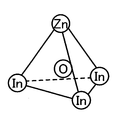
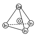
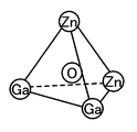
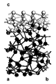
도 3a 내지 도 3c는 In-Ga-Zn-O계 산화물 반도체의 금속과 산소의 결정 구조를 도시한다;
도 4a 및 도 4b는 각각이 구조 모델을 나타내는 도면을 도시한다;
도 5a 및 도 5b는 각각이 구조 모델을 나타내는 도면을 도시한다;
도 6a 및 도 6b는 각각이 구조 모델을 나타내는 도면을 도시한다;
도 7a는 샘플 1의 C-V 특성을 나타내는 그래프를 도시하고, 도 7b는 샘플 1의 (Vg)와 (1/C)2 사이의 관계를 나타내는 그래프를 도시한다;
도 8a는 샘플 2의 C-V 특성을 나타내는 그래프를 도시하고, 도 8b는 샘플 2의 (Vg)와 (1/C)2 사이의 관계를 나타내는 그래프를 도시한다;
도 9는 루틸 구조(rutile structure)를 갖는 이산화 티타늄의 결정 구조를 도시한다;
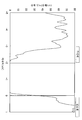
도 10은 루틸 구조를 갖는 이산화 티타늄의 상태 밀도를 도시한다;
도 11은 산소 결핍 상태의 루틸 구조를 갖는 이산화 티타늄의 상태 밀도를 도시한다;
도 12는 일산화 티타늄의 상태 밀도를 도시한다;
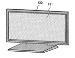
도 13a 및 도 13b 각각은 박막 트랜지스터를 적용한 전자 장치를 나타낸다;
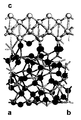
도 14는 In-Ga-Zn-O계 산화물 반도체를 포함하는 박막 트랜지스터의 TEM 사진이다.



Claims (8)
- 트랜지스터로서,
게이트 전극;
상기 게이트 전극과 중첩하는 게이트 절연막;
상기 게이트 절연막을 개재하여 상기 게이트 전극과 중첩하는 산화물 반도체막; 및
상기 산화물 반도체막과 중첩하는 티타늄막을 포함하고,
상기 산화물 반도체막은 인듐, 갈륨 및 아연 중 적어도 하나를 포함하고,
상기 산화물 반도체막은 제1 영역 및 제2 영역을 포함하고,
상기 제1 영역 및 상기 제2 영역은 상기 티타늄막과 중첩하고,
상기 제1 영역은 상기 제2 영역보다 상기 티타늄막에 근접하고,
상기 제1 영역은 상기 티타늄막의 부근에 있고,
상기 제1 영역에 있어서의 인듐의 농도는 상기 제2 영역에 있어서의 인듐의 농도보다 높은, 트랜지스터. - 트랜지스터로서,
게이트 전극;
상기 게이트 전극과 중첩하는 게이트 절연막;
상기 게이트 절연막을 개재하여 상기 게이트 전극과 중첩하는 산화물 반도체막;
상기 산화물 반도체막과 접하고, 티타늄 및 산소를 포함하는 막; 및
상기 막과 접하는 티타늄막을 포함하고,
상기 산화물 반도체막은 인듐, 갈륨 및 아연 중 적어도 하나를 포함하고,
상기 산화물 반도체막은 제1 영역 및 제2 영역을 포함하고,
상기 제1 영역 및 상기 제2 영역은 상기 막과 중첩하고,
상기 제1 영역은 상기 제2 영역보다 상기 막에 근접하고,
상기 제1 영역은 상기 막의 부근에 있고,
상기 제1 영역에 있어서의 인듐의 농도는 상기 제2 영역에 있어서의 인듐의 농도보다 높은, 트랜지스터. - 트랜지스터로서,
게이트 전극;
상기 게이트 전극과 중첩하는 게이트 절연막;
상기 게이트 절연막을 개재하여 상기 게이트 전극과 중첩하는 산화물 반도체막;
상기 산화물 반도체막과 접하고, 티타늄 및 산소를 포함하는 막; 및
상기 막과 접하는 티타늄막을 포함하고,
상기 산화물 반도체막은 인듐, 갈륨 및 아연 중 적어도 하나를 포함하고,
상기 산화물 반도체막은 제1 영역 및 제2 영역을 포함하고,
상기 제1 영역 및 상기 제2 영역은 상기 막과 중첩하고,
상기 제1 영역은 상기 제2 영역보다 상기 막에 근접하고,
상기 제1 영역은 상기 막의 부근에 있고,
상기 제1 영역에 있어서의 인듐, 갈륨 및 아연 중 어느 하나의 농도는 상기 제2 영역에 있어서의 그것의 농도보다 높고,
상기 제1 영역은 인듐, 갈륨 및 아연 중 어느 하나를 포함하는 결정립 또는 미결정을 포함하는, 트랜지스터. - 제1항 내지 제3항 중 어느 한 항에 있어서,
상기 트랜지스터의 타입은 보텀 게이트 타입(bottom gate type)인, 트랜지스터. - 제1항 내지 제3항 중 어느 한 항에 있어서,
상기 산화물 반도체막은 In-Ga-Zn-O계 산화물 반도체를 포함하는, 트랜지스터. - 제1항 내지 제3항 중 어느 한 항에 있어서,
상기 산화물 반도체막에서의 수소의 농도는 5×10¹⁶/cm3 미만인, 트랜지스터. - 제1항 내지 제3항 중 어느 한 항에 있어서,
상기 산화물 반도체막의 캐리어 밀도는 5×10¹⁰/cm3 이하인, 트랜지스터. - 제1항 내지 제3항 중 어느 한 항에 있어서,
상기 제1 영역은 인듐의 결정을 포함하는, 트랜지스터.
Applications Claiming Priority (3)
| Application Number | Priority Date | Filing Date | Title |
|---|---|---|---|
| JPJP-P-2009-265409 | 2009-11-20 | ||
| JP2009265409 | 2009-11-20 | ||
| PCT/JP2010/069391 WO2011062048A1 (en) | 2009-11-20 | 2010-10-26 | Thin film transistor |
Related Parent Applications (1)
| Application Number | Title | Priority Date | Filing Date |
|---|---|---|---|
| KR1020127013018A Division KR20120107079A (ko) | 2009-11-20 | 2010-10-26 | 박막 트랜지스터 |
Related Child Applications (1)
| Application Number | Title | Priority Date | Filing Date |
|---|---|---|---|
| KR1020167005690A Division KR102026212B1 (ko) | 2009-11-20 | 2010-10-26 | 트랜지스터 |
Publications (1)
| Publication Number | Publication Date |
|---|---|
| KR20140074404A true KR20140074404A (ko) | 2014-06-17 |
Family
ID=44059531
Family Applications (7)
| Application Number | Title | Priority Date | Filing Date |
|---|---|---|---|
| KR1020207030816A Ceased KR20200124769A (ko) | 2009-11-20 | 2010-10-26 | 트랜지스터 |
| KR1020147014982A Ceased KR20140074404A (ko) | 2009-11-20 | 2010-10-26 | 트랜지스터 |
| KR1020197027376A Ceased KR20190109597A (ko) | 2009-11-20 | 2010-10-26 | 트랜지스터 |
| KR1020167005690A Active KR102026212B1 (ko) | 2009-11-20 | 2010-10-26 | 트랜지스터 |
| KR1020127013018A Ceased KR20120107079A (ko) | 2009-11-20 | 2010-10-26 | 박막 트랜지스터 |
| KR1020227009107A Ceased KR20220041239A (ko) | 2009-11-20 | 2010-10-26 | 트랜지스터 |
| KR1020177027697A Expired - Fee Related KR101945660B1 (ko) | 2009-11-20 | 2010-10-26 | 트랜지스터 |
Family Applications Before (1)
| Application Number | Title | Priority Date | Filing Date |
|---|---|---|---|
| KR1020207030816A Ceased KR20200124769A (ko) | 2009-11-20 | 2010-10-26 | 트랜지스터 |
Family Applications After (5)
| Application Number | Title | Priority Date | Filing Date |
|---|---|---|---|
| KR1020197027376A Ceased KR20190109597A (ko) | 2009-11-20 | 2010-10-26 | 트랜지스터 |
| KR1020167005690A Active KR102026212B1 (ko) | 2009-11-20 | 2010-10-26 | 트랜지스터 |
| KR1020127013018A Ceased KR20120107079A (ko) | 2009-11-20 | 2010-10-26 | 박막 트랜지스터 |
| KR1020227009107A Ceased KR20220041239A (ko) | 2009-11-20 | 2010-10-26 | 트랜지스터 |
| KR1020177027697A Expired - Fee Related KR101945660B1 (ko) | 2009-11-20 | 2010-10-26 | 트랜지스터 |
Country Status (5)
| Country | Link |
|---|---|
| US (3) | US8766250B2 (ko) |
| JP (1) | JP5608520B2 (ko) |
| KR (7) | KR20200124769A (ko) |
| TW (3) | TWI529950B (ko) |
| WO (1) | WO2011062048A1 (ko) |
Cited By (1)
| Publication number | Priority date | Publication date | Assignee | Title |
|---|---|---|---|---|
| US9748402B2 (en) | 2015-02-04 | 2017-08-29 | Samsung Display Co., Ltd. | Semiconductor element and organic light emitting display device having a semiconductor element |
Families Citing this family (37)
| Publication number | Priority date | Publication date | Assignee | Title |
|---|---|---|---|---|
| EP2449593B1 (en) * | 2009-07-03 | 2019-08-28 | Semiconductor Energy Laboratory Co, Ltd. | Method for manufacturing semiconductor device |
| KR102577885B1 (ko) | 2009-10-16 | 2023-09-14 | 가부시키가이샤 한도오따이 에네루기 켄큐쇼 | 반도체 장치 |
| WO2011068022A1 (en) | 2009-12-04 | 2011-06-09 | Semiconductor Energy Laboratory Co., Ltd. | Semiconductor device |
| CN102939658B (zh) * | 2010-06-01 | 2014-03-26 | 夏普株式会社 | 薄膜晶体管 |
| US8895978B2 (en) | 2010-07-02 | 2014-11-25 | Advanced Interconnect Materials, Llc | Semiconductor device |
| WO2012056933A1 (ja) * | 2010-10-25 | 2012-05-03 | 株式会社日立製作所 | 酸化物半導体装置およびその製造方法 |
| JP2012169344A (ja) * | 2011-02-10 | 2012-09-06 | Sony Corp | 薄膜トランジスタならびに表示装置および電子機器 |
| US8659015B2 (en) * | 2011-03-04 | 2014-02-25 | Semiconductor Energy Laboratory Co., Ltd. | Semiconductor device |
| JP5429718B2 (ja) * | 2011-03-08 | 2014-02-26 | 合同会社先端配線材料研究所 | 酸化物半導体用電極、その形成方法 |
| US9496138B2 (en) * | 2011-07-08 | 2016-11-15 | Semiconductor Energy Laboratory Co., Ltd. | Method for manufacturing oxide semiconductor film, method for manufacturing semiconductor device, and semiconductor device |
| JP5917385B2 (ja) * | 2011-12-27 | 2016-05-11 | 株式会社半導体エネルギー研究所 | 半導体装置の作製方法 |
| TWI562361B (en) * | 2012-02-02 | 2016-12-11 | Semiconductor Energy Lab Co Ltd | Semiconductor device |
| JP6059566B2 (ja) * | 2012-04-13 | 2017-01-11 | 株式会社半導体エネルギー研究所 | 半導体装置の作製方法 |
| US9018624B2 (en) | 2012-09-13 | 2015-04-28 | Semiconductor Energy Laboratory Co., Ltd. | Display device and electronic appliance |
| JP6021586B2 (ja) | 2012-10-17 | 2016-11-09 | 株式会社半導体エネルギー研究所 | 半導体装置 |
| TWI527230B (zh) | 2012-10-19 | 2016-03-21 | 元太科技工業股份有限公司 | 薄膜電晶體結構及其製作方法 |
| US9246011B2 (en) * | 2012-11-30 | 2016-01-26 | Semiconductor Energy Laboratory Co., Ltd. | Semiconductor device |
| WO2014103901A1 (en) | 2012-12-25 | 2014-07-03 | Semiconductor Energy Laboratory Co., Ltd. | Semiconductor device and method for manufacturing the same |
| JP2015018939A (ja) * | 2013-07-11 | 2015-01-29 | ルネサスエレクトロニクス株式会社 | 半導体装置 |
| JP6180908B2 (ja) * | 2013-12-06 | 2017-08-16 | 富士フイルム株式会社 | 金属酸化物半導体膜、薄膜トランジスタ、表示装置、イメージセンサ及びx線センサ |
| KR102260886B1 (ko) * | 2014-12-10 | 2021-06-07 | 삼성디스플레이 주식회사 | 박막 트랜지스터 |
| US9761732B2 (en) | 2015-02-25 | 2017-09-12 | Snaptrack Inc. | Tunnel thin film transistor with hetero-junction structure |
| CN106887436B (zh) * | 2015-12-16 | 2019-10-25 | 鸿富锦精密工业(深圳)有限公司 | 薄膜晶体管阵列基板及其制备方法 |
| US10388738B2 (en) * | 2016-04-01 | 2019-08-20 | Semiconductor Energy Laboratory Co., Ltd. | Composite oxide semiconductor and method for manufacturing the same |
| CN107689391B (zh) * | 2016-08-04 | 2020-09-08 | 鸿富锦精密工业(深圳)有限公司 | 薄膜晶体管基板及其制备方法 |
| JP6268248B2 (ja) * | 2016-09-22 | 2018-01-24 | 株式会社半導体エネルギー研究所 | トランジスタの作製方法 |
| TW202129966A (zh) | 2016-10-21 | 2021-08-01 | 日商半導體能源研究所股份有限公司 | 複合氧化物及電晶體 |
| CN110383436A (zh) | 2017-03-13 | 2019-10-25 | 株式会社半导体能源研究所 | 复合氧化物及晶体管 |
| KR102263435B1 (ko) | 2017-09-13 | 2021-06-11 | 주식회사 엘지에너지솔루션 | 비딩부가 생략된 원통형 전지셀 |
| JP7398860B2 (ja) * | 2018-08-08 | 2023-12-15 | 株式会社ジャパンディスプレイ | 薄膜トランジスタの製造方法 |
| CN111725238B (zh) * | 2019-03-19 | 2023-08-15 | 群创光电股份有限公司 | 具有晶体管元件的工作模块 |
| TWI690060B (zh) | 2019-04-25 | 2020-04-01 | 元太科技工業股份有限公司 | 記憶體結構及其製造方法 |
| US20210376156A1 (en) * | 2020-05-29 | 2021-12-02 | Taiwan Semiconductor Manufacturing Company Limited | Raised source/drain oxide semiconducting thin film transistor and methods of making the same |
| US11984508B2 (en) * | 2021-02-24 | 2024-05-14 | Taiwan Semiconductor Manufacturing Company Limited | Thin film transistor including a compositionally-modulated active region and methods for forming the same |
| US20230092244A1 (en) * | 2021-09-22 | 2023-03-23 | Intel Corporation | Three-dimensional transistor with fin-shaped gate |
| JP2024035746A (ja) * | 2022-09-02 | 2024-03-14 | キオクシア株式会社 | 半導体装置 |
| JP2024073192A (ja) * | 2022-11-17 | 2024-05-29 | 株式会社ジャパンディスプレイ | 表示装置 |
Family Cites Families (117)
| Publication number | Priority date | Publication date | Assignee | Title |
|---|---|---|---|---|
| JPS60198861A (ja) | 1984-03-23 | 1985-10-08 | Fujitsu Ltd | 薄膜トランジスタ |
| JPH0244256B2 (ja) | 1987-01-28 | 1990-10-03 | Kagaku Gijutsucho Mukizaishitsu Kenkyushocho | Ingazn2o5deshimesarerurotsuhoshokeinosojokozoojusurukagobutsuoyobisonoseizoho |
| JPH0244260B2 (ja) | 1987-02-24 | 1990-10-03 | Kagaku Gijutsucho Mukizaishitsu Kenkyushocho | Ingazn5o8deshimesarerurotsuhoshokeinosojokozoojusurukagobutsuoyobisonoseizoho |
| JPH0244258B2 (ja) | 1987-02-24 | 1990-10-03 | Kagaku Gijutsucho Mukizaishitsu Kenkyushocho | Ingazn3o6deshimesarerurotsuhoshokeinosojokozoojusurukagobutsuoyobisonoseizoho |
| JPS63210023A (ja) | 1987-02-24 | 1988-08-31 | Natl Inst For Res In Inorg Mater | InGaZn↓4O↓7で示される六方晶系の層状構造を有する化合物およびその製造法 |
| JPH0244262B2 (ja) | 1987-02-27 | 1990-10-03 | Kagaku Gijutsucho Mukizaishitsu Kenkyushocho | Ingazn6o9deshimesarerurotsuhoshokeinosojokozoojusurukagobutsuoyobisonoseizoho |
| JPH0244263B2 (ja) | 1987-04-22 | 1990-10-03 | Kagaku Gijutsucho Mukizaishitsu Kenkyushocho | Ingazn7o10deshimesarerurotsuhoshokeinosojokozoojusurukagobutsuoyobisonoseizoho |
| JPH05251705A (ja) | 1992-03-04 | 1993-09-28 | Fuji Xerox Co Ltd | 薄膜トランジスタ |
| JP3479375B2 (ja) | 1995-03-27 | 2003-12-15 | 科学技術振興事業団 | 亜酸化銅等の金属酸化物半導体による薄膜トランジスタとpn接合を形成した金属酸化物半導体装置およびそれらの製造方法 |
| JPH11505377A (ja) | 1995-08-03 | 1999-05-18 | フィリップス エレクトロニクス ネムローゼ フェンノートシャップ | 半導体装置 |
| JP3625598B2 (ja) | 1995-12-30 | 2005-03-02 | 三星電子株式会社 | 液晶表示装置の製造方法 |
| JP4170454B2 (ja) | 1998-07-24 | 2008-10-22 | Hoya株式会社 | 透明導電性酸化物薄膜を有する物品及びその製造方法 |
| JP2000150861A (ja) | 1998-11-16 | 2000-05-30 | Tdk Corp | 酸化物薄膜 |
| JP3276930B2 (ja) | 1998-11-17 | 2002-04-22 | 科学技術振興事業団 | トランジスタ及び半導体装置 |
| TW460731B (en) | 1999-09-03 | 2001-10-21 | Ind Tech Res Inst | Electrode structure and production method of wide viewing angle LCD |
| JP4089858B2 (ja) | 2000-09-01 | 2008-05-28 | 国立大学法人東北大学 | 半導体デバイス |
| KR20020038482A (ko) | 2000-11-15 | 2002-05-23 | 모리시타 요이찌 | 박막 트랜지스터 어레이, 그 제조방법 및 그것을 이용한표시패널 |
| JP3997731B2 (ja) | 2001-03-19 | 2007-10-24 | 富士ゼロックス株式会社 | 基材上に結晶性半導体薄膜を形成する方法 |
| JP2002289859A (ja) | 2001-03-23 | 2002-10-04 | Minolta Co Ltd | 薄膜トランジスタ |
| JP3925839B2 (ja) | 2001-09-10 | 2007-06-06 | シャープ株式会社 | 半導体記憶装置およびその試験方法 |
| JP4090716B2 (ja) | 2001-09-10 | 2008-05-28 | 雅司 川崎 | 薄膜トランジスタおよびマトリクス表示装置 |
| JP4164562B2 (ja) | 2002-09-11 | 2008-10-15 | 独立行政法人科学技術振興機構 | ホモロガス薄膜を活性層として用いる透明薄膜電界効果型トランジスタ |
| EP1443130B1 (en) | 2001-11-05 | 2011-09-28 | Japan Science and Technology Agency | Natural superlattice homologous single crystal thin film, method for preparation thereof, and device using said single crystal thin film |
| JP4083486B2 (ja) | 2002-02-21 | 2008-04-30 | 独立行政法人科学技術振興機構 | LnCuO(S,Se,Te)単結晶薄膜の製造方法 |
| US7049190B2 (en) | 2002-03-15 | 2006-05-23 | Sanyo Electric Co., Ltd. | Method for forming ZnO film, method for forming ZnO semiconductor layer, method for fabricating semiconductor device, and semiconductor device |
| JP3933591B2 (ja) | 2002-03-26 | 2007-06-20 | 淳二 城戸 | 有機エレクトロルミネッセント素子 |
| US7339187B2 (en) | 2002-05-21 | 2008-03-04 | State Of Oregon Acting By And Through The Oregon State Board Of Higher Education On Behalf Of Oregon State University | Transistor structures |
| JP2004022625A (ja) | 2002-06-13 | 2004-01-22 | Murata Mfg Co Ltd | 半導体デバイス及び該半導体デバイスの製造方法 |
| US7105868B2 (en) | 2002-06-24 | 2006-09-12 | Cermet, Inc. | High-electron mobility transistor with zinc oxide |
| US7067843B2 (en) | 2002-10-11 | 2006-06-27 | E. I. Du Pont De Nemours And Company | Transparent oxide semiconductor thin film transistors |
| JP4166105B2 (ja) | 2003-03-06 | 2008-10-15 | シャープ株式会社 | 半導体装置およびその製造方法 |
| JP2004273732A (ja) | 2003-03-07 | 2004-09-30 | Sharp Corp | アクティブマトリクス基板およびその製造方法 |
| JP4108633B2 (ja) | 2003-06-20 | 2008-06-25 | シャープ株式会社 | 薄膜トランジスタおよびその製造方法ならびに電子デバイス |
| US7262463B2 (en) | 2003-07-25 | 2007-08-28 | Hewlett-Packard Development Company, L.P. | Transistor including a deposited channel region having a doped portion |
| EP1737044B1 (en) | 2004-03-12 | 2014-12-10 | Japan Science and Technology Agency | Amorphous oxide and thin film transistor |
| US7282782B2 (en) | 2004-03-12 | 2007-10-16 | Hewlett-Packard Development Company, L.P. | Combined binary oxide semiconductor device |
| US7145174B2 (en) | 2004-03-12 | 2006-12-05 | Hewlett-Packard Development Company, Lp. | Semiconductor device |
| US7297977B2 (en) | 2004-03-12 | 2007-11-20 | Hewlett-Packard Development Company, L.P. | Semiconductor device |
| US7211825B2 (en) | 2004-06-14 | 2007-05-01 | Yi-Chi Shih | Indium oxide-based thin film transistors and circuits |
| JP2006100760A (ja) | 2004-09-02 | 2006-04-13 | Casio Comput Co Ltd | 薄膜トランジスタおよびその製造方法 |
| US7285501B2 (en) | 2004-09-17 | 2007-10-23 | Hewlett-Packard Development Company, L.P. | Method of forming a solution processed device |
| US7298084B2 (en) | 2004-11-02 | 2007-11-20 | 3M Innovative Properties Company | Methods and displays utilizing integrated zinc oxide row and column drivers in conjunction with organic light emitting diodes |
| US7829444B2 (en) | 2004-11-10 | 2010-11-09 | Canon Kabushiki Kaisha | Field effect transistor manufacturing method |
| US7453065B2 (en) | 2004-11-10 | 2008-11-18 | Canon Kabushiki Kaisha | Sensor and image pickup device |
| RU2358354C2 (ru) | 2004-11-10 | 2009-06-10 | Кэнон Кабусики Кайся | Светоизлучающее устройство |
| EP1815530B1 (en) | 2004-11-10 | 2021-02-17 | Canon Kabushiki Kaisha | Field effect transistor employing an amorphous oxide |
| US7863611B2 (en) | 2004-11-10 | 2011-01-04 | Canon Kabushiki Kaisha | Integrated circuits utilizing amorphous oxides |
| KR100998527B1 (ko) * | 2004-11-10 | 2010-12-07 | 고쿠리츠다이가쿠호진 토쿄고교 다이가꾸 | 비정질 산화물 및 전계 효과 트랜지스터 |
| US7791072B2 (en) | 2004-11-10 | 2010-09-07 | Canon Kabushiki Kaisha | Display |
| US7579224B2 (en) | 2005-01-21 | 2009-08-25 | Semiconductor Energy Laboratory Co., Ltd. | Method for manufacturing a thin film semiconductor device |
| TWI481024B (zh) | 2005-01-28 | 2015-04-11 | 半導體能源研究所股份有限公司 | 半導體裝置,電子裝置,和半導體裝置的製造方法 |
| TWI505473B (zh) | 2005-01-28 | 2015-10-21 | 半導體能源研究所股份有限公司 | 半導體裝置,電子裝置,和半導體裝置的製造方法 |
| US7858451B2 (en) | 2005-02-03 | 2010-12-28 | Semiconductor Energy Laboratory Co., Ltd. | Electronic device, semiconductor device and manufacturing method thereof |
| US7948171B2 (en) | 2005-02-18 | 2011-05-24 | Semiconductor Energy Laboratory Co., Ltd. | Light emitting device |
| US20060197092A1 (en) | 2005-03-03 | 2006-09-07 | Randy Hoffman | System and method for forming conductive material on a substrate |
| US8681077B2 (en) | 2005-03-18 | 2014-03-25 | Semiconductor Energy Laboratory Co., Ltd. | Semiconductor device, and display device, driving method and electronic apparatus thereof |
| US7544967B2 (en) | 2005-03-28 | 2009-06-09 | Massachusetts Institute Of Technology | Low voltage flexible organic/transparent transistor for selective gas sensing, photodetecting and CMOS device applications |
| US7645478B2 (en) | 2005-03-31 | 2010-01-12 | 3M Innovative Properties Company | Methods of making displays |
| US8300031B2 (en) | 2005-04-20 | 2012-10-30 | Semiconductor Energy Laboratory Co., Ltd. | Semiconductor device comprising transistor having gate and drain connected through a current-voltage conversion element |
| JP2006344849A (ja) | 2005-06-10 | 2006-12-21 | Casio Comput Co Ltd | 薄膜トランジスタ |
| US7402506B2 (en) | 2005-06-16 | 2008-07-22 | Eastman Kodak Company | Methods of making thin film transistors comprising zinc-oxide-based semiconductor materials and transistors made thereby |
| US7691666B2 (en) | 2005-06-16 | 2010-04-06 | Eastman Kodak Company | Methods of making thin film transistors comprising zinc-oxide-based semiconductor materials and transistors made thereby |
| US7507618B2 (en) | 2005-06-27 | 2009-03-24 | 3M Innovative Properties Company | Method for making electronic devices using metal oxide nanoparticles |
| KR100711890B1 (ko) | 2005-07-28 | 2007-04-25 | 삼성에스디아이 주식회사 | 유기 발광표시장치 및 그의 제조방법 |
| JP2007059128A (ja) | 2005-08-23 | 2007-03-08 | Canon Inc | 有機el表示装置およびその製造方法 |
| JP4280736B2 (ja) | 2005-09-06 | 2009-06-17 | キヤノン株式会社 | 半導体素子 |
| JP4560502B2 (ja) | 2005-09-06 | 2010-10-13 | キヤノン株式会社 | 電界効果型トランジスタ |
| JP5116225B2 (ja) | 2005-09-06 | 2013-01-09 | キヤノン株式会社 | 酸化物半導体デバイスの製造方法 |
| JP4850457B2 (ja) | 2005-09-06 | 2012-01-11 | キヤノン株式会社 | 薄膜トランジスタ及び薄膜ダイオード |
| JP2007073705A (ja) | 2005-09-06 | 2007-03-22 | Canon Inc | 酸化物半導体チャネル薄膜トランジスタおよびその製造方法 |
| JP5064747B2 (ja) | 2005-09-29 | 2012-10-31 | 株式会社半導体エネルギー研究所 | 半導体装置、電気泳動表示装置、表示モジュール、電子機器、及び半導体装置の作製方法 |
| JP5078246B2 (ja) | 2005-09-29 | 2012-11-21 | 株式会社半導体エネルギー研究所 | 半導体装置、及び半導体装置の作製方法 |
| EP1998373A3 (en) | 2005-09-29 | 2012-10-31 | Semiconductor Energy Laboratory Co, Ltd. | Semiconductor device having oxide semiconductor layer and manufacturing method thereof |
| JP5037808B2 (ja) | 2005-10-20 | 2012-10-03 | キヤノン株式会社 | アモルファス酸化物を用いた電界効果型トランジスタ、及び該トランジスタを用いた表示装置 |
| CN101577231B (zh) | 2005-11-15 | 2013-01-02 | 株式会社半导体能源研究所 | 半导体器件及其制造方法 |
| TWI292281B (en) | 2005-12-29 | 2008-01-01 | Ind Tech Res Inst | Pixel structure of active organic light emitting diode and method of fabricating the same |
| US7867636B2 (en) | 2006-01-11 | 2011-01-11 | Murata Manufacturing Co., Ltd. | Transparent conductive film and method for manufacturing the same |
| JP4977478B2 (ja) | 2006-01-21 | 2012-07-18 | 三星電子株式会社 | ZnOフィルム及びこれを用いたTFTの製造方法 |
| US7576394B2 (en) | 2006-02-02 | 2009-08-18 | Kochi Industrial Promotion Center | Thin film transistor including low resistance conductive thin films and manufacturing method thereof |
| US7977169B2 (en) | 2006-02-15 | 2011-07-12 | Kochi Industrial Promotion Center | Semiconductor device including active layer made of zinc oxide with controlled orientations and manufacturing method thereof |
| KR20070101595A (ko) | 2006-04-11 | 2007-10-17 | 삼성전자주식회사 | ZnO TFT |
| US20070252928A1 (en) | 2006-04-28 | 2007-11-01 | Toppan Printing Co., Ltd. | Structure, transmission type liquid crystal display, reflection type display and manufacturing method thereof |
| JP5028033B2 (ja) | 2006-06-13 | 2012-09-19 | キヤノン株式会社 | 酸化物半導体膜のドライエッチング方法 |
| JP4999400B2 (ja) | 2006-08-09 | 2012-08-15 | キヤノン株式会社 | 酸化物半導体膜のドライエッチング方法 |
| JP4609797B2 (ja) | 2006-08-09 | 2011-01-12 | Nec液晶テクノロジー株式会社 | 薄膜デバイス及びその製造方法 |
| JP4332545B2 (ja) | 2006-09-15 | 2009-09-16 | キヤノン株式会社 | 電界効果型トランジスタ及びその製造方法 |
| JP4274219B2 (ja) | 2006-09-27 | 2009-06-03 | セイコーエプソン株式会社 | 電子デバイス、有機エレクトロルミネッセンス装置、有機薄膜半導体装置 |
| JP5164357B2 (ja) | 2006-09-27 | 2013-03-21 | キヤノン株式会社 | 半導体装置及び半導体装置の製造方法 |
| US7622371B2 (en) | 2006-10-10 | 2009-11-24 | Hewlett-Packard Development Company, L.P. | Fused nanocrystal thin film semiconductor and method |
| US7772021B2 (en) | 2006-11-29 | 2010-08-10 | Samsung Electronics Co., Ltd. | Flat panel displays comprising a thin-film transistor having a semiconductive oxide in its channel and methods of fabricating the same for use in flat panel displays |
| JP2008140684A (ja) | 2006-12-04 | 2008-06-19 | Toppan Printing Co Ltd | カラーelディスプレイおよびその製造方法 |
| KR101303578B1 (ko) | 2007-01-05 | 2013-09-09 | 삼성전자주식회사 | 박막 식각 방법 |
| US8207063B2 (en) | 2007-01-26 | 2012-06-26 | Eastman Kodak Company | Process for atomic layer deposition |
| US8129714B2 (en) | 2007-02-16 | 2012-03-06 | Idemitsu Kosan Co., Ltd. | Semiconductor, semiconductor device, complementary transistor circuit device |
| KR101410926B1 (ko) * | 2007-02-16 | 2014-06-24 | 삼성전자주식회사 | 박막 트랜지스터 및 그 제조방법 |
| WO2008099863A1 (ja) * | 2007-02-16 | 2008-08-21 | Idemitsu Kosan Co., Ltd. | 半導体,半導体装置及び相補型トランジスタ回路装置 |
| KR100858088B1 (ko) * | 2007-02-28 | 2008-09-10 | 삼성전자주식회사 | 박막 트랜지스터 및 그 제조 방법 |
| KR100851215B1 (ko) | 2007-03-14 | 2008-08-07 | 삼성에스디아이 주식회사 | 박막 트랜지스터 및 이를 이용한 유기 전계 발광표시장치 |
| JP5197058B2 (ja) * | 2007-04-09 | 2013-05-15 | キヤノン株式会社 | 発光装置とその作製方法 |
| JP2008270313A (ja) * | 2007-04-17 | 2008-11-06 | Matsushita Electric Ind Co Ltd | 半導体記憶素子 |
| US7795613B2 (en) | 2007-04-17 | 2010-09-14 | Toppan Printing Co., Ltd. | Structure with transistor |
| KR101325053B1 (ko) | 2007-04-18 | 2013-11-05 | 삼성디스플레이 주식회사 | 박막 트랜지스터 기판 및 이의 제조 방법 |
| KR20080094300A (ko) | 2007-04-19 | 2008-10-23 | 삼성전자주식회사 | 박막 트랜지스터 및 그 제조 방법과 박막 트랜지스터를포함하는 평판 디스플레이 |
| KR101334181B1 (ko) | 2007-04-20 | 2013-11-28 | 삼성전자주식회사 | 선택적으로 결정화된 채널층을 갖는 박막 트랜지스터 및 그제조 방법 |
| WO2008133345A1 (en) | 2007-04-25 | 2008-11-06 | Canon Kabushiki Kaisha | Oxynitride semiconductor |
| KR101345376B1 (ko) | 2007-05-29 | 2013-12-24 | 삼성전자주식회사 | ZnO 계 박막 트랜지스터 및 그 제조방법 |
| JP5213421B2 (ja) | 2007-12-04 | 2013-06-19 | キヤノン株式会社 | 酸化物半導体薄膜トランジスタ |
| US8202365B2 (en) | 2007-12-17 | 2012-06-19 | Fujifilm Corporation | Process for producing oriented inorganic crystalline film, and semiconductor device using the oriented inorganic crystalline film |
| JP4623179B2 (ja) | 2008-09-18 | 2011-02-02 | ソニー株式会社 | 薄膜トランジスタおよびその製造方法 |
| JP5451280B2 (ja) | 2008-10-09 | 2014-03-26 | キヤノン株式会社 | ウルツ鉱型結晶成長用基板およびその製造方法ならびに半導体装置 |
| JP5504008B2 (ja) * | 2009-03-06 | 2014-05-28 | 株式会社半導体エネルギー研究所 | 半導体装置 |
| KR102329380B1 (ko) | 2009-10-09 | 2021-11-22 | 가부시키가이샤 한도오따이 에네루기 켄큐쇼 | 반도체 장치 |
| WO2011043164A1 (en) | 2009-10-09 | 2011-04-14 | Semiconductor Energy Laboratory Co., Ltd. | Semiconductor device and method for manufacturing the semiconductor device |
| CN102598279B (zh) | 2009-11-06 | 2015-10-07 | 株式会社半导体能源研究所 | 半导体装置 |
| KR102066532B1 (ko) | 2009-11-06 | 2020-01-15 | 가부시키가이샤 한도오따이 에네루기 켄큐쇼 | 반도체 장치 |
| WO2011058865A1 (en) * | 2009-11-13 | 2011-05-19 | Semiconductor Energy Laboratory Co., Ltd. | Semiconductor devi ce |
| JP5612299B2 (ja) * | 2009-11-20 | 2014-10-22 | 株式会社半導体エネルギー研究所 | トランジスタの作製方法 |
-
2010
- 2010-10-26 KR KR1020207030816A patent/KR20200124769A/ko not_active Ceased
- 2010-10-26 KR KR1020147014982A patent/KR20140074404A/ko not_active Ceased
- 2010-10-26 KR KR1020197027376A patent/KR20190109597A/ko not_active Ceased
- 2010-10-26 KR KR1020167005690A patent/KR102026212B1/ko active Active
- 2010-10-26 KR KR1020127013018A patent/KR20120107079A/ko not_active Ceased
- 2010-10-26 KR KR1020227009107A patent/KR20220041239A/ko not_active Ceased
- 2010-10-26 KR KR1020177027697A patent/KR101945660B1/ko not_active Expired - Fee Related
- 2010-10-26 WO PCT/JP2010/069391 patent/WO2011062048A1/en not_active Ceased
- 2010-11-16 JP JP2010255538A patent/JP5608520B2/ja active Active
- 2010-11-19 TW TW104112315A patent/TWI529950B/zh active
- 2010-11-19 US US12/950,186 patent/US8766250B2/en active Active
- 2010-11-19 TW TW105102038A patent/TWI580039B/zh active
- 2010-11-19 TW TW099139943A patent/TWI491046B/zh active
-
2014
- 2014-06-06 US US14/297,733 patent/US8963149B2/en active Active
-
2015
- 2015-02-13 US US14/621,838 patent/US9306075B2/en active Active
Cited By (1)
| Publication number | Priority date | Publication date | Assignee | Title |
|---|---|---|---|---|
| US9748402B2 (en) | 2015-02-04 | 2017-08-29 | Samsung Display Co., Ltd. | Semiconductor element and organic light emitting display device having a semiconductor element |
Also Published As
| Publication number | Publication date |
|---|---|
| KR20160031047A (ko) | 2016-03-21 |
| KR102026212B1 (ko) | 2019-09-27 |
| TWI491046B (zh) | 2015-07-01 |
| US8766250B2 (en) | 2014-07-01 |
| TWI580039B (zh) | 2017-04-21 |
| JP5608520B2 (ja) | 2014-10-15 |
| US20140284601A1 (en) | 2014-09-25 |
| TW201631762A (zh) | 2016-09-01 |
| TW201130139A (en) | 2011-09-01 |
| KR20200124769A (ko) | 2020-11-03 |
| JP2011129897A (ja) | 2011-06-30 |
| WO2011062048A1 (en) | 2011-05-26 |
| TW201530781A (zh) | 2015-08-01 |
| KR20190109597A (ko) | 2019-09-25 |
| KR20170117208A (ko) | 2017-10-20 |
| KR101945660B1 (ko) | 2019-02-07 |
| KR20120107079A (ko) | 2012-09-28 |
| KR20220041239A (ko) | 2022-03-31 |
| US20150162450A1 (en) | 2015-06-11 |
| US8963149B2 (en) | 2015-02-24 |
| US20110121289A1 (en) | 2011-05-26 |
| TWI529950B (zh) | 2016-04-11 |
| US9306075B2 (en) | 2016-04-05 |
Similar Documents
| Publication | Publication Date | Title |
|---|---|---|
| KR101945660B1 (ko) | 트랜지스터 | |
| JP7153111B2 (ja) | 半導体装置 | |
| KR102655144B1 (ko) | 반도체 장치 및 그 제작 방법 | |
| JP6411820B2 (ja) | 半導体装置および半導体装置の作製方法 | |
| KR102103913B1 (ko) | 반도체 장치 및 반도체 장치의 제작 방법 | |
| KR102219628B1 (ko) | 반도체 장치 및 반도체 장치의 제작 방법 | |
| KR102112872B1 (ko) | 반도체 장치 및 반도체 장치의 제작 방법 | |
| KR20190105544A (ko) | 반도체 장치 | |
| KR20120103754A (ko) | 반도체 장치 | |
| JP5657878B2 (ja) | トランジスタの作製方法 | |
| CN116344345B (zh) | 铁电场效应晶体管及其制备方法和铁电存储器 | |
| JP5612299B2 (ja) | トランジスタの作製方法 | |
| JP5940124B2 (ja) | トランジスタの作製方法 | |
| JP6046794B2 (ja) | トランジスタの作製方法 | |
| JP2015062250A (ja) | トランジスタ | |
| TW202535799A (zh) | 氧化物半導體薄膜、半導體元件及其製造方法,以及濺鍍靶材及濺鍍靶材之製造方法 | |
| CN121442746A (zh) | 一种半导体薄膜晶体管及其制备方法 |
Legal Events
| Date | Code | Title | Description |
|---|---|---|---|
| A107 | Divisional application of patent | ||
| A201 | Request for examination | ||
| PA0104 | Divisional application for international application |
Comment text: Divisional Application for International Patent Patent event code: PA01041R01D Patent event date: 20140602 Application number text: 1020127013018 Filing date: 20120521 |
|
| PA0201 | Request for examination | ||
| PG1501 | Laying open of application | ||
| E902 | Notification of reason for refusal | ||
| PE0902 | Notice of grounds for rejection |
Comment text: Notification of reason for refusal Patent event date: 20150824 Patent event code: PE09021S01D |
|
| AMND | Amendment | ||
| E601 | Decision to refuse application | ||
| PE0601 | Decision on rejection of patent |
Patent event date: 20160201 Comment text: Decision to Refuse Application Patent event code: PE06012S01D Patent event date: 20150824 Comment text: Notification of reason for refusal Patent event code: PE06011S01I |
|
| A107 | Divisional application of patent | ||
| AMND | Amendment | ||
| PA0104 | Divisional application for international application |
Comment text: Divisional Application for International Patent Patent event code: PA01041R01D Patent event date: 20160302 Application number text: 1020127013018 Filing date: 20120521 |
|
| PX0901 | Re-examination |
Patent event code: PX09011S01I Patent event date: 20160201 Comment text: Decision to Refuse Application Patent event code: PX09012R01I Patent event date: 20151026 Comment text: Amendment to Specification, etc. |
|
| E90F | Notification of reason for final refusal | ||
| PE0902 | Notice of grounds for rejection |
Comment text: Final Notice of Reason for Refusal Patent event date: 20160319 Patent event code: PE09021S02D |
|
| AMND | Amendment | ||
| E801 | Decision on dismissal of amendment | ||
| PE0801 | Dismissal of amendment |
Patent event code: PE08012E01D Comment text: Decision on Dismissal of Amendment Patent event date: 20160913 Patent event code: PE08011R01I Comment text: Amendment to Specification, etc. Patent event date: 20160519 Patent event code: PE08011R01I Comment text: Amendment to Specification, etc. Patent event date: 20160302 Patent event code: PE08011R01I Comment text: Amendment to Specification, etc. Patent event date: 20151026 |
|
| PX0601 | Decision of rejection after re-examination |
Comment text: Decision to Refuse Application Patent event code: PX06014S01D Patent event date: 20160913 Comment text: Amendment to Specification, etc. Patent event code: PX06012R01I Patent event date: 20160519 Comment text: Final Notice of Reason for Refusal Patent event code: PX06013S02I Patent event date: 20160319 Comment text: Amendment to Specification, etc. Patent event code: PX06012R01I Patent event date: 20160302 Comment text: Decision to Refuse Application Patent event code: PX06011S01I Patent event date: 20160201 Comment text: Amendment to Specification, etc. Patent event code: PX06012R01I Patent event date: 20151026 Comment text: Notification of reason for refusal Patent event code: PX06013S01I Patent event date: 20150824 |
|
| J201 | Request for trial against refusal decision | ||
| PJ0201 | Trial against decision of rejection |
Patent event date: 20161019 Comment text: Request for Trial against Decision on Refusal Patent event code: PJ02012R01D Patent event date: 20160913 Comment text: Decision to Refuse Application Patent event code: PJ02011S01I Patent event date: 20160201 Comment text: Decision to Refuse Application Patent event code: PJ02011S01I Appeal kind category: Appeal against decision to decline refusal Appeal identifier: 2016101005972 Request date: 20161019 |
|
| J301 | Trial decision |
Free format text: TRIAL NUMBER: 2016101005972; TRIAL DECISION FOR APPEAL AGAINST DECISION TO DECLINE REFUSAL REQUESTED 20161019 Effective date: 20180816 |
|
| PJ1301 | Trial decision |
Patent event code: PJ13011S01D Patent event date: 20180816 Comment text: Trial Decision on Objection to Decision on Refusal Appeal kind category: Appeal against decision to decline refusal Request date: 20161019 Decision date: 20180816 Appeal identifier: 2016101005972 |