KR20140084076A - 이방성 도전 접착제 및 그의 제조 방법, 발광 장치 및 그의 제조 방법 - Google Patents
이방성 도전 접착제 및 그의 제조 방법, 발광 장치 및 그의 제조 방법 Download PDFInfo
- Publication number
- KR20140084076A KR20140084076A KR1020147011209A KR20147011209A KR20140084076A KR 20140084076 A KR20140084076 A KR 20140084076A KR 1020147011209 A KR1020147011209 A KR 1020147011209A KR 20147011209 A KR20147011209 A KR 20147011209A KR 20140084076 A KR20140084076 A KR 20140084076A
- Authority
- KR
- South Korea
- Prior art keywords
- light
- anisotropic conductive
- conductive adhesive
- light emitting
- metal layer
- Prior art date
- Legal status (The legal status is an assumption and is not a legal conclusion. Google has not performed a legal analysis and makes no representation as to the accuracy of the status listed.)
- Granted
Links
Images
Classifications
-
- H—ELECTRICITY
- H01—ELECTRIC ELEMENTS
- H01B—CABLES; CONDUCTORS; INSULATORS; SELECTION OF MATERIALS FOR THEIR CONDUCTIVE, INSULATING OR DIELECTRIC PROPERTIES
- H01B1/00—Conductors or conductive bodies characterised by the conductive materials; Selection of materials as conductors
- H01B1/20—Conductive material dispersed in non-conductive organic material
- H01B1/22—Conductive material dispersed in non-conductive organic material the conductive material comprising metals or alloys
-
- H—ELECTRICITY
- H10—SEMICONDUCTOR DEVICES; ELECTRIC SOLID-STATE DEVICES NOT OTHERWISE PROVIDED FOR
- H10H—INORGANIC LIGHT-EMITTING SEMICONDUCTOR DEVICES HAVING POTENTIAL BARRIERS
- H10H20/00—Individual inorganic light-emitting semiconductor devices having potential barriers, e.g. light-emitting diodes [LED]
- H10H20/80—Constructional details
- H10H20/84—Coatings, e.g. passivation layers or antireflective coatings
- H10H20/841—Reflective coatings, e.g. dielectric Bragg reflectors
-
- C—CHEMISTRY; METALLURGY
- C09—DYES; PAINTS; POLISHES; NATURAL RESINS; ADHESIVES; COMPOSITIONS NOT OTHERWISE PROVIDED FOR; APPLICATIONS OF MATERIALS NOT OTHERWISE PROVIDED FOR
- C09J—ADHESIVES; NON-MECHANICAL ASPECTS OF ADHESIVE PROCESSES IN GENERAL; ADHESIVE PROCESSES NOT PROVIDED FOR ELSEWHERE; USE OF MATERIALS AS ADHESIVES
- C09J11/00—Features of adhesives not provided for in group C09J9/00, e.g. additives
-
- C—CHEMISTRY; METALLURGY
- C09—DYES; PAINTS; POLISHES; NATURAL RESINS; ADHESIVES; COMPOSITIONS NOT OTHERWISE PROVIDED FOR; APPLICATIONS OF MATERIALS NOT OTHERWISE PROVIDED FOR
- C09J—ADHESIVES; NON-MECHANICAL ASPECTS OF ADHESIVE PROCESSES IN GENERAL; ADHESIVE PROCESSES NOT PROVIDED FOR ELSEWHERE; USE OF MATERIALS AS ADHESIVES
- C09J9/00—Adhesives characterised by their physical nature or the effects produced, e.g. glue sticks
-
- H—ELECTRICITY
- H10—SEMICONDUCTOR DEVICES; ELECTRIC SOLID-STATE DEVICES NOT OTHERWISE PROVIDED FOR
- H10H—INORGANIC LIGHT-EMITTING SEMICONDUCTOR DEVICES HAVING POTENTIAL BARRIERS
- H10H20/00—Individual inorganic light-emitting semiconductor devices having potential barriers, e.g. light-emitting diodes [LED]
- H10H20/80—Constructional details
- H10H20/85—Packages
- H10H20/857—Interconnections, e.g. lead-frames, bond wires or solder balls
-
- H—ELECTRICITY
- H10—SEMICONDUCTOR DEVICES; ELECTRIC SOLID-STATE DEVICES NOT OTHERWISE PROVIDED FOR
- H10H—INORGANIC LIGHT-EMITTING SEMICONDUCTOR DEVICES HAVING POTENTIAL BARRIERS
- H10H20/00—Individual inorganic light-emitting semiconductor devices having potential barriers, e.g. light-emitting diodes [LED]
- H10H20/80—Constructional details
- H10H20/85—Packages
- H10H20/855—Optical field-shaping means, e.g. lenses
- H10H20/856—Reflecting means
-
- H—ELECTRICITY
- H10—SEMICONDUCTOR DEVICES; ELECTRIC SOLID-STATE DEVICES NOT OTHERWISE PROVIDED FOR
- H10W—GENERIC PACKAGES, INTERCONNECTIONS, CONNECTORS OR OTHER CONSTRUCTIONAL DETAILS OF DEVICES COVERED BY CLASS H10
- H10W72/00—Interconnections or connectors in packages
- H10W72/071—Connecting or disconnecting
- H10W72/075—Connecting or disconnecting of bond wires
- H10W72/07551—Connecting or disconnecting of bond wires characterised by changes in properties of the bond wires during the connecting
- H10W72/07554—Connecting or disconnecting of bond wires characterised by changes in properties of the bond wires during the connecting changes in dispositions
-
- H—ELECTRICITY
- H10—SEMICONDUCTOR DEVICES; ELECTRIC SOLID-STATE DEVICES NOT OTHERWISE PROVIDED FOR
- H10W—GENERIC PACKAGES, INTERCONNECTIONS, CONNECTORS OR OTHER CONSTRUCTIONAL DETAILS OF DEVICES COVERED BY CLASS H10
- H10W72/00—Interconnections or connectors in packages
- H10W72/50—Bond wires
- H10W72/541—Dispositions of bond wires
- H10W72/547—Dispositions of multiple bond wires
-
- H—ELECTRICITY
- H10—SEMICONDUCTOR DEVICES; ELECTRIC SOLID-STATE DEVICES NOT OTHERWISE PROVIDED FOR
- H10W—GENERIC PACKAGES, INTERCONNECTIONS, CONNECTORS OR OTHER CONSTRUCTIONAL DETAILS OF DEVICES COVERED BY CLASS H10
- H10W72/00—Interconnections or connectors in packages
- H10W72/851—Dispositions of multiple connectors or interconnections
- H10W72/874—On different surfaces
- H10W72/884—Die-attach connectors and bond wires
-
- H—ELECTRICITY
- H10—SEMICONDUCTOR DEVICES; ELECTRIC SOLID-STATE DEVICES NOT OTHERWISE PROVIDED FOR
- H10W—GENERIC PACKAGES, INTERCONNECTIONS, CONNECTORS OR OTHER CONSTRUCTIONAL DETAILS OF DEVICES COVERED BY CLASS H10
- H10W74/00—Encapsulations, e.g. protective coatings
- H10W74/10—Encapsulations, e.g. protective coatings characterised by their shape or disposition
- H10W74/15—Encapsulations, e.g. protective coatings characterised by their shape or disposition on active surfaces of flip-chip devices, e.g. underfills
-
- H—ELECTRICITY
- H10—SEMICONDUCTOR DEVICES; ELECTRIC SOLID-STATE DEVICES NOT OTHERWISE PROVIDED FOR
- H10W—GENERIC PACKAGES, INTERCONNECTIONS, CONNECTORS OR OTHER CONSTRUCTIONAL DETAILS OF DEVICES COVERED BY CLASS H10
- H10W90/00—Package configurations
- H10W90/701—Package configurations characterised by the relative positions of pads or connectors relative to package parts
- H10W90/721—Package configurations characterised by the relative positions of pads or connectors relative to package parts of bump connectors
- H10W90/724—Package configurations characterised by the relative positions of pads or connectors relative to package parts of bump connectors between a chip and a stacked insulating package substrate, interposer or RDL
-
- H—ELECTRICITY
- H10—SEMICONDUCTOR DEVICES; ELECTRIC SOLID-STATE DEVICES NOT OTHERWISE PROVIDED FOR
- H10W—GENERIC PACKAGES, INTERCONNECTIONS, CONNECTORS OR OTHER CONSTRUCTIONAL DETAILS OF DEVICES COVERED BY CLASS H10
- H10W90/00—Package configurations
- H10W90/701—Package configurations characterised by the relative positions of pads or connectors relative to package parts
- H10W90/731—Package configurations characterised by the relative positions of pads or connectors relative to package parts of die-attach connectors
- H10W90/734—Package configurations characterised by the relative positions of pads or connectors relative to package parts of die-attach connectors between a chip and a stacked insulating package substrate, interposer or RDL
-
- H—ELECTRICITY
- H10—SEMICONDUCTOR DEVICES; ELECTRIC SOLID-STATE DEVICES NOT OTHERWISE PROVIDED FOR
- H10W—GENERIC PACKAGES, INTERCONNECTIONS, CONNECTORS OR OTHER CONSTRUCTIONAL DETAILS OF DEVICES COVERED BY CLASS H10
- H10W90/00—Package configurations
- H10W90/701—Package configurations characterised by the relative positions of pads or connectors relative to package parts
- H10W90/751—Package configurations characterised by the relative positions of pads or connectors relative to package parts of bond wires
- H10W90/754—Package configurations characterised by the relative positions of pads or connectors relative to package parts of bond wires between a chip and a stacked insulating package substrate, interposer or RDL
Landscapes
- Chemical & Material Sciences (AREA)
- Organic Chemistry (AREA)
- Physics & Mathematics (AREA)
- Dispersion Chemistry (AREA)
- Spectroscopy & Molecular Physics (AREA)
- Led Device Packages (AREA)
- Adhesives Or Adhesive Processes (AREA)
- Conductive Materials (AREA)
Abstract
Description
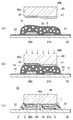
도 2(a) 내지 도 2(c)는 본 발명의 발광 장치의 제조 공정의 실시 형태를 도시하는 도면이다.
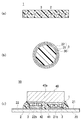
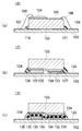
도 3(a)는 와이어 본딩에 의한 실장 방법을 도시하는 도면이다. 도 3(b)는 도전성 페이스트에 의한 실장 방법을 도시하는 도면이다. 도 3(c)는 이방성 도전 접착제에 의한 실장 방법을 도시하는 도면이다.

2…절연성 접착제 수지
3…도전성 입자
10…발광 장치
20…배선 기판
21…제1 접속 전극
22…제2 접속 전극
30…수지 입자
31…광 반사성 금속층
32…피복층
40…발광 소자
41…제1 접속 전극
42…제2 접속 전극
Claims (5)
- 절연성 접착제 수지 중에 광 반사성의 도전성 입자를 함유하는 이방성 도전 접착제이며,
상기 광 반사성의 도전성 입자가, 핵이 되는 수지 입자의 표면에 피크 파장 460nm에 있어서의 반사율이 60% 이상인 금속으로 이루어지는 광 반사성 금속층이 형성되고, 상기 광 반사성 금속층의 표면에 은 합금으로 이루어지는 피복층이 형성되어 이루어지는 이방성 도전 접착제. - 제1항에 있어서, 상기 광 반사성 금속층은 니켈, 금, 은으로 이루어지는 군으로부터 선택되는 1 또는 2 이상의 금속으로 이루어지는 이방성 도전 접착제.
- 이방성 도전 접착제를 제조하는 방법이며,
상기 이방성 도전 접착제는, 절연성 접착제 수지 중에 광 반사성의 도전성 입자를 함유하고, 상기 광 반사성의 도전성 입자가, 핵이 되는 수지 입자의 표면에 피크 파장 460nm에 있어서의 반사율이 60% 이상인 금속으로 이루어지는 광 반사성 금속층이 형성되고, 상기 광 반사성 금속층의 표면에 은 합금으로 이루어지는 피복층이 형성되어 이루어지고,
상기 광 반사성 금속층을 도금법에 의해 형성하는 공정을 갖는 이방성 도전 접착제의 제조 방법. - 쌍이 되는 접속 전극을 갖는 배선 기판과,
상기 배선 기판의 쌍이 되는 접속 전극에 각각 대응하는 접속 전극을 갖는 발광 소자를 구비하고,
절연성 접착제 수지 중에 광 반사성의 도전성 입자를 함유하고, 상기 광 반사성의 도전성 입자가, 핵이 되는 수지 입자의 표면에 피크 파장 460nm에 있어서의 반사율이 60% 이상인 금속으로 이루어지는 광 반사성 금속층이 형성되고, 상기 광 반사성 금속층의 표면에 은 합금으로 이루어지는 피복층이 형성되어 이루어지는 이방성 도전 접착제에 의해 상기 발광 소자가 상기 배선 기판 상에 접착되고, 상기 발광 소자의 접속 전극이, 상기 이방성 도전 접착제의 도전성 입자를 통해 상기 배선 기판의 대응하는 접속 전극에 대하여 각각 전기적으로 접속되어 있는 발광 장치. - 쌍이 되는 접속 전극을 갖는 배선 기판과, 상기 배선 기판의 접속 전극에 각각 대응하는 접속 전극을 갖는 발광 소자를 준비하고,
상기 배선 기판의 접속 전극과 상기 발광 소자의 접속 전극을 대향하는 방향으로 배치한 상태에서, 상기 발광 소자와 상기 발광 소자 사이에 이방성 도전 접착제를 배치하고, 상기 이방성 도전 접착제는 절연성 접착제 수지 중에 광 반사성의 도전성 입자를 함유하고, 상기 광 반사성의 도전성 입자가, 핵이 되는 수지 입자의 표면에 피크 파장 460nm에 있어서의 반사율이 60% 이상인 금속으로 이루어지는 광 반사성 금속층이 형성되고, 상기 광 반사성 금속층의 표면에 은 합금으로 이루어지는 피복층이 형성되어 이루어지고,
상기 배선 기판에 대하여 상기 발광 소자를 열 압착하는 공정을 갖는 발광 소자의 제조 방법.
Applications Claiming Priority (3)
| Application Number | Priority Date | Filing Date | Title |
|---|---|---|---|
| JPJP-P-2011-222498 | 2011-10-07 | ||
| JP2011222498A JP5916334B2 (ja) | 2011-10-07 | 2011-10-07 | 異方性導電接着剤及びその製造方法、発光装置及びその製造方法 |
| PCT/JP2012/076011 WO2013051708A1 (ja) | 2011-10-07 | 2012-10-05 | 異方性導電接着剤及びその製造方法、発光装置及びその製造方法 |
Publications (2)
| Publication Number | Publication Date |
|---|---|
| KR20140084076A true KR20140084076A (ko) | 2014-07-04 |
| KR102010103B1 KR102010103B1 (ko) | 2019-08-12 |
Family
ID=48043861
Family Applications (1)
| Application Number | Title | Priority Date | Filing Date |
|---|---|---|---|
| KR1020147011209A Active KR102010103B1 (ko) | 2011-10-07 | 2012-10-05 | 이방성 도전 접착제 및 그의 제조 방법, 발광 장치 및 그의 제조 방법 |
Country Status (7)
| Country | Link |
|---|---|
| US (1) | US20140217450A1 (ko) |
| EP (1) | EP2765173A4 (ko) |
| JP (1) | JP5916334B2 (ko) |
| KR (1) | KR102010103B1 (ko) |
| CN (1) | CN104039914B (ko) |
| TW (1) | TWI559334B (ko) |
| WO (1) | WO2013051708A1 (ko) |
Families Citing this family (32)
| Publication number | Priority date | Publication date | Assignee | Title |
|---|---|---|---|---|
| JP5965199B2 (ja) * | 2012-04-17 | 2016-08-03 | デクセリアルズ株式会社 | 異方性導電接着剤及びその製造方法、発光装置及びその製造方法 |
| US9269681B2 (en) * | 2012-11-16 | 2016-02-23 | Qualcomm Incorporated | Surface finish on trace for a thermal compression flip chip (TCFC) |
| JP5985414B2 (ja) * | 2013-02-19 | 2016-09-06 | デクセリアルズ株式会社 | 異方性導電接着剤、発光装置及び異方性導電接着剤の製造方法 |
| CN105009314B (zh) * | 2013-02-27 | 2019-11-05 | 日亚化学工业株式会社 | 发光装置、发光元件安装方法以及发光元件用安装装置 |
| EP3051598A4 (en) * | 2013-09-26 | 2017-06-28 | Dexerials Corporation | Light emitting device, anisotropic conductive adhesive and method for manufacturing light emitting device |
| TWI707484B (zh) * | 2013-11-14 | 2020-10-11 | 晶元光電股份有限公司 | 發光裝置 |
| JP6324746B2 (ja) * | 2014-02-03 | 2018-05-16 | デクセリアルズ株式会社 | 接続体、接続体の製造方法、電子機器 |
| JP6347635B2 (ja) * | 2014-03-19 | 2018-06-27 | デクセリアルズ株式会社 | 異方性導電接着剤 |
| US10283685B2 (en) * | 2014-09-26 | 2019-05-07 | Seoul Viosys Co., Ltd. | Light emitting device and method of fabricating the same |
| CN105493297B (zh) * | 2015-05-21 | 2018-09-11 | 歌尔股份有限公司 | 微发光二极管的转移方法、制造方法、装置和电子设备 |
| DE102015112967A1 (de) * | 2015-08-06 | 2017-02-09 | Osram Opto Semiconductors Gmbh | Verfahren zum Herstellen eines optoelektronischen Bauelements und optoelektronisches Bauelement |
| JP2017157724A (ja) * | 2016-03-02 | 2017-09-07 | デクセリアルズ株式会社 | 表示装置及びその製造方法、並びに発光装置及びその製造方法 |
| DE102016106494A1 (de) * | 2016-04-08 | 2017-10-12 | Osram Opto Semiconductors Gmbh | Optoelektronisches bauelement und verfahren zum herstellen eines optoelektronischen bauelements |
| KR102555383B1 (ko) * | 2016-12-07 | 2023-07-12 | 엘지디스플레이 주식회사 | 유기발광소자를 이용한 조명장치 및 그 제조방법 |
| JP7314801B2 (ja) * | 2017-12-28 | 2023-07-26 | 株式会社レゾナック | 接続構造体及びその製造方法 |
| JP7046351B2 (ja) | 2018-01-31 | 2022-04-04 | 三国電子有限会社 | 接続構造体の作製方法 |
| JP7185252B2 (ja) | 2018-01-31 | 2022-12-07 | 三国電子有限会社 | 接続構造体の作製方法 |
| JP7160302B2 (ja) * | 2018-01-31 | 2022-10-25 | 三国電子有限会社 | 接続構造体および接続構造体の作製方法 |
| JP7093639B2 (ja) * | 2018-02-06 | 2022-06-30 | 三菱マテリアル株式会社 | 銀被覆樹脂粒子 |
| CN113930167B (zh) * | 2018-03-01 | 2023-06-23 | 住友电木株式会社 | 糊状粘接剂组合物和半导体装置 |
| CN111788275B (zh) * | 2018-03-01 | 2021-12-03 | 住友电木株式会社 | 糊状粘接剂组合物和半导体装置 |
| JP7348478B2 (ja) * | 2018-07-09 | 2023-09-21 | 日亜化学工業株式会社 | 発光装置及びその製造方法 |
| TWI671921B (zh) * | 2018-09-14 | 2019-09-11 | 頎邦科技股份有限公司 | 晶片封裝構造及其晶片 |
| JP7366337B2 (ja) * | 2018-12-25 | 2023-10-23 | 日亜化学工業株式会社 | 光源装置の製造方法および光源装置 |
| EP3675190B1 (en) | 2018-12-25 | 2023-05-03 | Nichia Corporation | Method of manufacturing light source device and light source device |
| TWI690102B (zh) * | 2019-01-04 | 2020-04-01 | 友達光電股份有限公司 | 發光裝置及其製造方法 |
| JP7298256B2 (ja) * | 2019-04-11 | 2023-06-27 | 株式会社レゾナック | 導電粒子 |
| JP7292669B2 (ja) * | 2019-04-11 | 2023-06-19 | 株式会社レゾナック | 導電粒子の製造方法 |
| KR102862766B1 (ko) * | 2019-05-29 | 2025-09-22 | 삼성전자주식회사 | 마이크로 엘이디 디스플레이 및 이의 제작 방법 |
| CN111574937B (zh) * | 2020-05-15 | 2021-10-08 | 武汉华星光电半导体显示技术有限公司 | 一种异方性导电胶、显示面板及显示装置 |
| DE102021120689A1 (de) * | 2021-08-09 | 2023-02-09 | OSRAM Opto Semiconductors Gesellschaft mit beschränkter Haftung | Transferverfahren für optoelektronsiche halbleiterbauelemete |
| KR20240038495A (ko) * | 2022-09-16 | 2024-03-25 | 삼성전자주식회사 | 고반사율 이방성 도전 필름 및 이를 포함하는 디스플레이 모듈 |
Citations (7)
| Publication number | Priority date | Publication date | Assignee | Title |
|---|---|---|---|---|
| JPH05152464A (ja) | 1991-11-25 | 1993-06-18 | Sumitomo Bakelite Co Ltd | 光半導体封止用エポキシ樹脂組成物 |
| JPH07157720A (ja) * | 1993-12-03 | 1995-06-20 | Sumitomo Bakelite Co Ltd | 異方導電フィルム |
| JP2002260446A (ja) * | 2001-02-27 | 2002-09-13 | Sekisui Chem Co Ltd | 導電性微粒子及び導電接続構造体 |
| JP2003026763A (ja) | 2001-07-13 | 2003-01-29 | New Japan Chem Co Ltd | エポキシ樹脂組成物 |
| JP2005120375A (ja) | 2003-10-14 | 2005-05-12 | Bayer Ag | 精製されたエラストマーの製造方法、及び精製されたエラストマー、及び前記のエラストマーから得られる製品 |
| JP2008266671A (ja) | 2007-04-16 | 2008-11-06 | Sony Corp | 銀系薄膜合金 |
| WO2011030621A1 (ja) * | 2009-09-14 | 2011-03-17 | ソニーケミカル&インフォメーションデバイス株式会社 | 光反射性異方性導電接着剤及び発光装置 |
Family Cites Families (19)
| Publication number | Priority date | Publication date | Assignee | Title |
|---|---|---|---|---|
| JP3284262B2 (ja) * | 1996-09-05 | 2002-05-20 | セイコーエプソン株式会社 | 液晶表示装置及びそれを用いた電子機器 |
| WO1999001519A1 (fr) * | 1997-07-04 | 1999-01-14 | Nippon Zeon Co., Ltd. | Adhesif pour composants semi-conducteurs |
| US5990498A (en) * | 1997-09-16 | 1999-11-23 | Polaroid Corporation | Light-emitting diode having uniform irradiance distribution |
| JP2001234152A (ja) * | 2000-02-24 | 2001-08-28 | Sumitomo Metal Mining Co Ltd | 導電性接着剤 |
| JP4660065B2 (ja) * | 2000-08-04 | 2011-03-30 | 積水化学工業株式会社 | 導電性微粒子及び基板構成体 |
| EP1626400A4 (en) * | 2003-05-22 | 2008-05-14 | Ricoh Kk | OPTICAL RECORDING MEDIUM |
| WO2005002002A1 (ja) * | 2003-06-25 | 2005-01-06 | Hitachi Chemical Co., Ltd. | 回路接続材料、これを用いたフィルム状回路接続材料、回路部材の接続構造及びその製造方法 |
| JP4433876B2 (ja) * | 2004-05-18 | 2010-03-17 | 住友金属鉱山株式会社 | エポキシ樹脂組成物及びそれを用いた光半導体用接着剤 |
| EP1783783A1 (en) * | 2004-08-05 | 2007-05-09 | Sekisui Chemical Co., Ltd. | Conductive fine particle, method for producing conductive fine particle and electroless silver plating liquid |
| JP4802666B2 (ja) * | 2005-11-08 | 2011-10-26 | 住友金属鉱山株式会社 | エポキシ樹脂接着組成物及びそれを用いた光半導体用接着剤 |
| JP2007258324A (ja) * | 2006-03-22 | 2007-10-04 | Matsushita Electric Ind Co Ltd | 発光装置の製造方法および発光装置 |
| JP5430093B2 (ja) * | 2008-07-24 | 2014-02-26 | デクセリアルズ株式会社 | 導電性粒子、異方性導電フィルム、及び接合体、並びに、接続方法 |
| WO2010029175A1 (en) * | 2008-09-12 | 2010-03-18 | Modpro Ab | Detection method and device based on nanoparticle aggregation |
| JP5526698B2 (ja) * | 2009-10-16 | 2014-06-18 | デクセリアルズ株式会社 | 光反射性導電粒子、異方性導電接着剤及び発光装置 |
| JP2011186414A (ja) * | 2010-02-12 | 2011-09-22 | Sony Corp | 光学素子、日射遮蔽装置、建具、窓材および光学素子の製造方法 |
| JP5745776B2 (ja) * | 2010-03-15 | 2015-07-08 | デクセリアルズ株式会社 | 光学積層体および建具 |
| JP5586300B2 (ja) * | 2010-03-31 | 2014-09-10 | デクセリアルズ株式会社 | 機能性積層体及び機能性構造体 |
| JP5583613B2 (ja) * | 2011-02-04 | 2014-09-03 | 株式会社日本触媒 | 導電性微粒子 |
| JP5609716B2 (ja) * | 2011-03-07 | 2014-10-22 | デクセリアルズ株式会社 | 光反射性異方性導電接着剤及び発光装置 |
-
2011
- 2011-10-07 JP JP2011222498A patent/JP5916334B2/ja active Active
-
2012
- 2012-10-05 KR KR1020147011209A patent/KR102010103B1/ko active Active
- 2012-10-05 TW TW101136830A patent/TWI559334B/zh active
- 2012-10-05 WO PCT/JP2012/076011 patent/WO2013051708A1/ja not_active Ceased
- 2012-10-05 CN CN201280060251.8A patent/CN104039914B/zh active Active
- 2012-10-05 EP EP12838614.1A patent/EP2765173A4/en not_active Withdrawn
-
2014
- 2014-04-07 US US14/246,618 patent/US20140217450A1/en not_active Abandoned
Patent Citations (7)
| Publication number | Priority date | Publication date | Assignee | Title |
|---|---|---|---|---|
| JPH05152464A (ja) | 1991-11-25 | 1993-06-18 | Sumitomo Bakelite Co Ltd | 光半導体封止用エポキシ樹脂組成物 |
| JPH07157720A (ja) * | 1993-12-03 | 1995-06-20 | Sumitomo Bakelite Co Ltd | 異方導電フィルム |
| JP2002260446A (ja) * | 2001-02-27 | 2002-09-13 | Sekisui Chem Co Ltd | 導電性微粒子及び導電接続構造体 |
| JP2003026763A (ja) | 2001-07-13 | 2003-01-29 | New Japan Chem Co Ltd | エポキシ樹脂組成物 |
| JP2005120375A (ja) | 2003-10-14 | 2005-05-12 | Bayer Ag | 精製されたエラストマーの製造方法、及び精製されたエラストマー、及び前記のエラストマーから得られる製品 |
| JP2008266671A (ja) | 2007-04-16 | 2008-11-06 | Sony Corp | 銀系薄膜合金 |
| WO2011030621A1 (ja) * | 2009-09-14 | 2011-03-17 | ソニーケミカル&インフォメーションデバイス株式会社 | 光反射性異方性導電接着剤及び発光装置 |
Also Published As
| Publication number | Publication date |
|---|---|
| JP5916334B2 (ja) | 2016-05-11 |
| TWI559334B (zh) | 2016-11-21 |
| JP2013082784A (ja) | 2013-05-09 |
| KR102010103B1 (ko) | 2019-08-12 |
| WO2013051708A1 (ja) | 2013-04-11 |
| TW201331955A (zh) | 2013-08-01 |
| EP2765173A4 (en) | 2015-04-29 |
| US20140217450A1 (en) | 2014-08-07 |
| CN104039914B (zh) | 2016-08-24 |
| CN104039914A (zh) | 2014-09-10 |
| EP2765173A1 (en) | 2014-08-13 |
Similar Documents
| Publication | Publication Date | Title |
|---|---|---|
| KR20140084076A (ko) | 이방성 도전 접착제 및 그의 제조 방법, 발광 장치 및 그의 제조 방법 | |
| TWI579366B (zh) | 異向性導電接著劑及其製造方法、發光裝置及其製造方法 | |
| JP5985414B2 (ja) | 異方性導電接着剤、発光装置及び異方性導電接着剤の製造方法 | |
| TWI534839B (zh) | Light reflective conductive particles, anisotropic conductive adhesives and light-emitting devices | |
| US9670385B2 (en) | Anisotropic conductive adhesive | |
| TWI597346B (zh) | Anisotropic conductive adhesive and connecting structure | |
| EP3051598A1 (en) | Light emitting device, anisotropic conductive adhesive and method for manufacturing light emitting device | |
| KR20130088003A (ko) | 광반사성 이방성 도전 페이스트 및 발광 장치 | |
| KR20130049689A (ko) | 광반사성 이방성 도전 접착제 및 발광 장치 | |
| TW201418407A (zh) | 光反射性異向性導電接著劑及發光裝置 | |
| JP2014160708A (ja) | 異方性導電接着剤、発光装置及び異方性導電接着剤の製造方法 | |
| JP5381684B2 (ja) | 発光装置の製造方法 | |
| JP2014030026A (ja) | 異方性導電接着剤及び発光装置 | |
| HK1178320B (en) | Light-reflective anisotropic conductive adhesive agent, and light emitting device |
Legal Events
| Date | Code | Title | Description |
|---|---|---|---|
| PA0105 | International application |
Patent event date: 20140425 Patent event code: PA01051R01D Comment text: International Patent Application |
|
| PG1501 | Laying open of application | ||
| A201 | Request for examination | ||
| PA0201 | Request for examination |
Patent event code: PA02012R01D Patent event date: 20170620 Comment text: Request for Examination of Application |
|
| E902 | Notification of reason for refusal | ||
| PE0902 | Notice of grounds for rejection |
Comment text: Notification of reason for refusal Patent event date: 20181128 Patent event code: PE09021S01D |
|
| E701 | Decision to grant or registration of patent right | ||
| PE0701 | Decision of registration |
Patent event code: PE07011S01D Comment text: Decision to Grant Registration Patent event date: 20190513 |
|
| GRNT | Written decision to grant | ||
| PR0701 | Registration of establishment |
Comment text: Registration of Establishment Patent event date: 20190806 Patent event code: PR07011E01D |
|
| PR1002 | Payment of registration fee |
Payment date: 20190806 End annual number: 3 Start annual number: 1 |
|
| PG1601 | Publication of registration | ||
| PR1001 | Payment of annual fee |
Payment date: 20220701 Start annual number: 4 End annual number: 4 |
|
| PR1001 | Payment of annual fee |
Payment date: 20230705 Start annual number: 5 End annual number: 5 |