KR20140090176A - 도전 시트 및 터치 패널 - Google Patents
도전 시트 및 터치 패널 Download PDFInfo
- Publication number
- KR20140090176A KR20140090176A KR1020147011932A KR20147011932A KR20140090176A KR 20140090176 A KR20140090176 A KR 20140090176A KR 1020147011932 A KR1020147011932 A KR 1020147011932A KR 20147011932 A KR20147011932 A KR 20147011932A KR 20140090176 A KR20140090176 A KR 20140090176A
- Authority
- KR
- South Korea
- Prior art keywords
- electrode
- pattern
- conductive sheet
- electrode pattern
- conductive
- Prior art date
- Legal status (The legal status is an assumption and is not a legal conclusion. Google has not performed a legal analysis and makes no representation as to the accuracy of the status listed.)
- Granted
Links
Images




Classifications
-
- G—PHYSICS
- G06—COMPUTING OR CALCULATING; COUNTING
- G06F—ELECTRIC DIGITAL DATA PROCESSING
- G06F3/00—Input arrangements for transferring data to be processed into a form capable of being handled by the computer; Output arrangements for transferring data from processing unit to output unit, e.g. interface arrangements
- G06F3/01—Input arrangements or combined input and output arrangements for interaction between user and computer
- G06F3/03—Arrangements for converting the position or the displacement of a member into a coded form
- G06F3/041—Digitisers, e.g. for touch screens or touch pads, characterised by the transducing means
- G06F3/044—Digitisers, e.g. for touch screens or touch pads, characterised by the transducing means by capacitive means
- G06F3/0445—Digitisers, e.g. for touch screens or touch pads, characterised by the transducing means by capacitive means using two or more layers of sensing electrodes, e.g. using two layers of electrodes separated by a dielectric layer
-
- B—PERFORMING OPERATIONS; TRANSPORTING
- B32—LAYERED PRODUCTS
- B32B—LAYERED PRODUCTS, i.e. PRODUCTS BUILT-UP OF STRATA OF FLAT OR NON-FLAT, e.g. CELLULAR OR HONEYCOMB, FORM
- B32B15/00—Layered products comprising a layer of metal
- B32B15/14—Layered products comprising a layer of metal next to a fibrous or filamentary layer
-
- G—PHYSICS
- G06—COMPUTING OR CALCULATING; COUNTING
- G06F—ELECTRIC DIGITAL DATA PROCESSING
- G06F3/00—Input arrangements for transferring data to be processed into a form capable of being handled by the computer; Output arrangements for transferring data from processing unit to output unit, e.g. interface arrangements
- G06F3/01—Input arrangements or combined input and output arrangements for interaction between user and computer
- G06F3/03—Arrangements for converting the position or the displacement of a member into a coded form
- G06F3/041—Digitisers, e.g. for touch screens or touch pads, characterised by the transducing means
-
- G—PHYSICS
- G06—COMPUTING OR CALCULATING; COUNTING
- G06F—ELECTRIC DIGITAL DATA PROCESSING
- G06F3/00—Input arrangements for transferring data to be processed into a form capable of being handled by the computer; Output arrangements for transferring data from processing unit to output unit, e.g. interface arrangements
- G06F3/01—Input arrangements or combined input and output arrangements for interaction between user and computer
- G06F3/03—Arrangements for converting the position or the displacement of a member into a coded form
- G06F3/041—Digitisers, e.g. for touch screens or touch pads, characterised by the transducing means
- G06F3/044—Digitisers, e.g. for touch screens or touch pads, characterised by the transducing means by capacitive means
- G06F3/0446—Digitisers, e.g. for touch screens or touch pads, characterised by the transducing means by capacitive means using a grid-like structure of electrodes in at least two directions, e.g. using row and column electrodes
-
- H—ELECTRICITY
- H05—ELECTRIC TECHNIQUES NOT OTHERWISE PROVIDED FOR
- H05K—PRINTED CIRCUITS; CASINGS OR CONSTRUCTIONAL DETAILS OF ELECTRIC APPARATUS; MANUFACTURE OF ASSEMBLAGES OF ELECTRICAL COMPONENTS
- H05K1/00—Printed circuits
- H05K1/02—Details
- H05K1/0274—Optical details, e.g. printed circuits comprising integral optical means
-
- H—ELECTRICITY
- H05—ELECTRIC TECHNIQUES NOT OTHERWISE PROVIDED FOR
- H05K—PRINTED CIRCUITS; CASINGS OR CONSTRUCTIONAL DETAILS OF ELECTRIC APPARATUS; MANUFACTURE OF ASSEMBLAGES OF ELECTRICAL COMPONENTS
- H05K1/00—Printed circuits
- H05K1/02—Details
- H05K1/0296—Conductive pattern lay-out details not covered by sub groups H05K1/02 - H05K1/0295
-
- G—PHYSICS
- G06—COMPUTING OR CALCULATING; COUNTING
- G06F—ELECTRIC DIGITAL DATA PROCESSING
- G06F2203/00—Indexing scheme relating to G06F3/00 - G06F3/048
- G06F2203/041—Indexing scheme relating to G06F3/041 - G06F3/045
- G06F2203/04103—Manufacturing, i.e. details related to manufacturing processes specially suited for touch sensitive devices
-
- G—PHYSICS
- G06—COMPUTING OR CALCULATING; COUNTING
- G06F—ELECTRIC DIGITAL DATA PROCESSING
- G06F2203/00—Indexing scheme relating to G06F3/00 - G06F3/048
- G06F2203/041—Indexing scheme relating to G06F3/041 - G06F3/045
- G06F2203/04111—Cross over in capacitive digitiser, i.e. details of structures for connecting electrodes of the sensing pattern where the connections cross each other, e.g. bridge structures comprising an insulating layer, or vias through substrate
-
- G—PHYSICS
- G06—COMPUTING OR CALCULATING; COUNTING
- G06F—ELECTRIC DIGITAL DATA PROCESSING
- G06F2203/00—Indexing scheme relating to G06F3/00 - G06F3/048
- G06F2203/041—Indexing scheme relating to G06F3/041 - G06F3/045
- G06F2203/04112—Electrode mesh in capacitive digitiser: electrode for touch sensing is formed of a mesh of very fine, normally metallic, interconnected lines that are almost invisible to see. This provides a quite large but transparent electrode surface, without need for ITO or similar transparent conductive material
-
- H—ELECTRICITY
- H05—ELECTRIC TECHNIQUES NOT OTHERWISE PROVIDED FOR
- H05K—PRINTED CIRCUITS; CASINGS OR CONSTRUCTIONAL DETAILS OF ELECTRIC APPARATUS; MANUFACTURE OF ASSEMBLAGES OF ELECTRICAL COMPONENTS
- H05K2201/00—Indexing scheme relating to printed circuits covered by H05K1/00
- H05K2201/09—Shape and layout
- H05K2201/09209—Shape and layout details of conductors
- H05K2201/09218—Conductive traces
- H05K2201/09245—Crossing layout
Landscapes
- Engineering & Computer Science (AREA)
- General Engineering & Computer Science (AREA)
- Theoretical Computer Science (AREA)
- Human Computer Interaction (AREA)
- Physics & Mathematics (AREA)
- General Physics & Mathematics (AREA)
- Microelectronics & Electronic Packaging (AREA)
- Position Input By Displaying (AREA)
- Manufacture Of Macromolecular Shaped Articles (AREA)
- Non-Insulated Conductors (AREA)
Abstract
Description
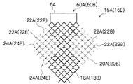
도 2 는 터치 패널용 도전 시트의 전극 단자의 다른 예를 나타내는 평면도이다.
도 3 은 터치 패널용 도전 시트의 전극 단자의 다른 예를 나타내는 평면도이다.
도 4a 는 터치 패널용 도전 시트를 일부 생략하여 나타내는 분해 사시도 (파트 1).
도 4b 는 터치 패널용 도전 시트를 일부 생략하여 나타내는 분해 사시도 (파트 2).
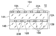
도 5a 는 터치 패널용 도전 시트의 일례를 일부 생략하여 나타내는 단면도이다.
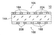
도 5b 는 터치 패널용 도전 시트의 다른 예를 일부 생략하여 나타내는 단면도이다.
도 6a 는 제 1 도전 시트에 형성되는 제 1 전극 패턴의 예를 나타내는 평면도이다.
도 6b 는 제 2 도전 시트에 형성되는 제 2 전극 패턴의 예를 나타내는 평면도이다.
도 7 은 제 1 도전 시트와 제 2 도전 시트를 조합하여 형성한 터치 패널용 도전 시트의 예를 일부 생략하여 나타내는 평면도이다.

12A : (제 1) 도전 시트 12B : (제 2) 도전 시트
14A : (제 1) 투명 기재 14B : (제 2) 투명 기재
16A : (제 1) 전극 패턴 16B : (제 2) 전극 패턴
18A : (제 1) 도전 패턴 18B : (제 2) 도전 패턴
20A : (제 1) 비도전 패턴 20B : (제 2) 비도전 패턴
22A : 단선부 22B : 단선부
24A : 격자 24B : 격자
60A : (제 1) 전극 단자 60B : (제 2) 전극 단자
62A : (제 1) 외부 배선 62B : (제 2) 외부 배선
64 : 프레임 형상 66 : 메시 형상
68 : 격자 70 : 조합 패턴
Claims (12)
- 금속 세선으로 구성된 전극 패턴; 및
상기 전극 패턴의 단부에 전기적으로 접속된 전극 단자를 포함하는 도전 시트로서,
상기 전극 패턴의 투과율이 83 % 이상이며, 상기 전극 패턴의 투과율을 a % 로 나타낼 때에, 상기 전극 단자의 투과율은 (a-20) % 이상 (a-3) % 이하인, 도전 시트. - 금속 세선으로 구성된 전극 패턴; 및
상기 전극 패턴의 단부에 전기적으로 접속된 전극 단자를 포함하는 도전 시트로서,
상기 전극 패턴의 개구율이 90 % 이상이며, 상기 전극 패턴의 개구율을 b % 로 나타낼 때에, 상기 전극 단자의 개구율은 (b-20) % 이상 (b-0.1) % 이하인, 도전 시트. - 제 1 항 또는 제 2 항에 있어서,
상기 전극 단자는 금속 세선으로 구성된 격자들로 이루어진 메시 형상을 포함하는, 도전 시트. - 제 3 항에 있어서,
상기 금속 세선은 30 ㎛ 이하의 선폭을 갖는, 도전 시트. - 제 3 항에 있어서,
상기 금속 세선은 불투명한 재료로 구성되는, 도전 시트. - 센싱 영역에 제공되고 금속 세선으로 구성된 전극 패턴; 및 상기 센싱 영역의 외측에 제공되고 상기 전극 패턴의 단부에 전기적으로 접속된 전극 단자를 포함하는 도전 시트를 갖는 터치 패널로서,
상기 전극 패턴의 투과율이 83 % 이상이며, 상기 전극 패턴의 투과율을 a % 로 나타낼 때에, 상기 전극 단자의 투과율은 (a-20) % 이상 (a-3) % 이하인, 터치 패널. - 센싱 영역에 제공되고 금속 세선으로 구성된 전극 패턴; 및 상기 센싱 영역의 외측에 제공되고 상기 전극 패턴의 단부에 전기적으로 접속된 전극 단자를 포함하는 도전 시트를 갖는 터치 패널로서,
상기 전극 패턴의 개구율이 90 % 이상이며, 상기 전극 패턴의 개구율을 b % 로 나타낼 때에, 상기 전극 단자의 개구율은 (b-20) % 이상 (b-0.1) % 이하인, 터치 패널. - 금속 세선으로 구성된 전극 패턴; 및
상기 전극 패턴의 단부에 전기적으로 접속된 전극 단자를 포함하는 도전 시트로서,
상기 전극 단자는, 금속 세선으로 구성된 프레임 형상을 포함하는, 도전 시트. - 제 8 항에 있어서,
상기 전극 패턴의 세선의 선폭을 a ㎛ 로 나타낼 때에, 상기 전극 단자의 프레임 형상의 선폭 b ㎛ 는 b ≥ 2a 또는 b ≥ a+5 (㎛) 를 만족하는, 도전 시트. - 제 9 항에 있어서,
상기 전극 패턴의 세선의 선폭 a ㎛ 는 30 ㎛ 이하인, 도전 시트. - 제 9 항 또는 제 10 항에 있어서,
상기 전극 단자의 금속 세선으로 구성된 프레임 형상 내에 제공되고, 금속 세선으로 구성된 격자들로 이루어진 메시 형상을 더 포함하는, 도전 시트. - 센싱 영역에 제공되고 금속 세선으로 구성된 전극 패턴; 및 상기 센싱 영역의 외측에 제공되고 상기 전극 패턴의 단부에 전기적으로 접속된 전극 단자를 포함하는 도전 시트를 갖는 터치 패널로서,
상기 전극 단자는, 금속 세선으로 구성된 프레임 형상을 포함하는, 터치 패널.
Applications Claiming Priority (7)
| Application Number | Priority Date | Filing Date | Title |
|---|---|---|---|
| JP2011276070A JP5509186B2 (ja) | 2011-12-16 | 2011-12-16 | タッチパネル及びタッチパネル用導電シート |
| JPJP-P-2011-276069 | 2011-12-16 | ||
| JP2011276069A JP5777251B2 (ja) | 2011-12-16 | 2011-12-16 | タッチパネル用導電シート及びタッチパネル |
| JPJP-P-2011-276070 | 2011-12-16 | ||
| JP2011281926A JP5748647B2 (ja) | 2011-12-22 | 2011-12-22 | 導電シート及びタッチパネル |
| JPJP-P-2011-281926 | 2011-12-22 | ||
| PCT/JP2012/082030 WO2013089085A1 (ja) | 2011-12-16 | 2012-12-11 | 導電シート及びタッチパネル |
Related Parent Applications (1)
| Application Number | Title | Priority Date | Filing Date |
|---|---|---|---|
| KR1020147011920A Division KR101451075B1 (ko) | 2011-12-16 | 2012-12-11 | 도전 시트 및 터치 패널 |
Publications (2)
| Publication Number | Publication Date |
|---|---|
| KR20140090176A true KR20140090176A (ko) | 2014-07-16 |
| KR101645828B1 KR101645828B1 (ko) | 2016-08-04 |
Family
ID=48612532
Family Applications (2)
| Application Number | Title | Priority Date | Filing Date |
|---|---|---|---|
| KR1020147011920A Active KR101451075B1 (ko) | 2011-12-16 | 2012-12-11 | 도전 시트 및 터치 패널 |
| KR1020147011932A Active KR101645828B1 (ko) | 2011-12-16 | 2012-12-11 | 도전 시트 및 터치 패널 |
Family Applications Before (1)
| Application Number | Title | Priority Date | Filing Date |
|---|---|---|---|
| KR1020147011920A Active KR101451075B1 (ko) | 2011-12-16 | 2012-12-11 | 도전 시트 및 터치 패널 |
Country Status (7)
| Country | Link |
|---|---|
| US (2) | US9055680B2 (ko) |
| EP (2) | EP2765490B1 (ko) |
| KR (2) | KR101451075B1 (ko) |
| CN (2) | CN103984461B (ko) |
| BR (1) | BR112014010102A8 (ko) |
| TW (2) | TWI537779B (ko) |
| WO (1) | WO2013089085A1 (ko) |
Families Citing this family (38)
| Publication number | Priority date | Publication date | Assignee | Title |
|---|---|---|---|---|
| CN103984461B (zh) | 2011-12-16 | 2017-09-15 | 富士胶片株式会社 | 导电片以及触摸面板 |
| WO2014115832A1 (ja) * | 2013-01-25 | 2014-07-31 | 凸版印刷株式会社 | タッチパネル、および、表示装置 |
| US20140251672A1 (en) * | 2013-03-05 | 2014-09-11 | Ronald Steven Cok | Micro-channel connection pad |
| TWI498799B (zh) * | 2013-03-27 | 2015-09-01 | Innolux Corp | 觸控元件及使用此觸控元件的電子裝置 |
| CN105210016B (zh) * | 2013-05-16 | 2017-10-17 | 三菱制纸株式会社 | 导电图案和单层电容式触摸屏的电极图案 |
| KR102053258B1 (ko) | 2013-07-16 | 2019-12-06 | 엘지이노텍 주식회사 | 터치 윈도우 |
| JP6026003B2 (ja) | 2013-10-22 | 2016-11-16 | 富士フイルム株式会社 | 導電性フイルム、タッチパネル及び表示装置 |
| KR102191575B1 (ko) * | 2014-01-13 | 2020-12-15 | 엘지이노텍 주식회사 | 터치 윈도우 및 이를 포함하는 디스플레이 장치 |
| JP6200582B2 (ja) * | 2014-04-08 | 2017-09-20 | 株式会社フジクラ | 配線体及び配線基板 |
| WO2015186276A1 (ja) * | 2014-06-02 | 2015-12-10 | 凸版印刷株式会社 | タッチセンサ用電極、タッチパネル、および、表示装置 |
| KR101802690B1 (ko) * | 2014-06-10 | 2017-11-28 | 후지필름 가부시키가이샤 | 터치 패널용 도전성 적층체, 터치 패널, 투명 도전성 적층체 |
| KR102256461B1 (ko) * | 2014-10-10 | 2021-05-26 | 삼성디스플레이 주식회사 | 터치 센서 및 이를 포함하는 표시 장치 |
| WO2016068161A1 (ja) * | 2014-10-28 | 2016-05-06 | コニカミノルタ株式会社 | パターン、パターン付き基材及びタッチパネル |
| JP6422762B2 (ja) * | 2014-12-16 | 2018-11-14 | 三菱製紙株式会社 | 光透過性導電材料 |
| TWI610204B (zh) | 2015-02-27 | 2018-01-01 | Fujikura Ltd | 配線體、配線基板以及碰觸偵知器 |
| CN106796477B (zh) * | 2015-02-27 | 2018-05-29 | 株式会社藤仓 | 布线体、布线基板、布线构造体及触摸传感器 |
| KR102255445B1 (ko) * | 2015-03-30 | 2021-05-21 | 동우 화인켐 주식회사 | 터치 센서 |
| KR102255415B1 (ko) * | 2015-03-30 | 2021-05-21 | 동우 화인켐 주식회사 | 터치 센서 |
| KR102372334B1 (ko) | 2015-04-14 | 2022-03-08 | 삼성디스플레이 주식회사 | 터치 패널 |
| JP2016206754A (ja) * | 2015-04-16 | 2016-12-08 | 凸版印刷株式会社 | タッチセンサ用電極、タッチパネル、および、表示装置 |
| KR102286210B1 (ko) * | 2015-05-04 | 2021-08-05 | 엘지이노텍 주식회사 | 터치 패널 |
| WO2016178498A1 (en) * | 2015-05-04 | 2016-11-10 | Lg Innotek Co., Ltd. | Touch panel |
| JP6421077B2 (ja) * | 2015-05-19 | 2018-11-07 | 富士フイルム株式会社 | アンテナの製造方法およびタッチセンサ |
| TWI610206B (zh) | 2015-06-22 | 2018-01-01 | Fujikura Ltd | 配線體、配線基板及觸控感測器 |
| JP6755000B2 (ja) * | 2016-03-28 | 2020-09-16 | パナソニックIpマネジメント株式会社 | タッチパネルセンサー用部材及びタッチパネル |
| JP6744169B2 (ja) * | 2016-04-04 | 2020-08-19 | 株式会社ジャパンディスプレイ | 検出装置及び表示装置 |
| US10126899B2 (en) | 2016-04-04 | 2018-11-13 | Japan Display Inc. | Detection device and display device |
| JPWO2018146963A1 (ja) * | 2017-02-09 | 2019-11-21 | コニカミノルタ株式会社 | タッチスクリーン及びタッチスクリーンの製造方法 |
| CN109558024B (zh) * | 2017-09-27 | 2024-05-17 | 京东方科技集团股份有限公司 | 显示装置、触控面板及其制造方法、驱动方法 |
| JP6886907B2 (ja) | 2017-10-31 | 2021-06-16 | 日本航空電子工業株式会社 | タッチパネル及びタッチパネルの生産方法 |
| CN109976566B (zh) * | 2018-03-23 | 2021-05-18 | 京东方科技集团股份有限公司 | 触控结构、触控基板及其制作方法、显示装置 |
| JP7115036B2 (ja) * | 2018-05-25 | 2022-08-09 | ウシオ電機株式会社 | エキシマランプ |
| JP6658800B2 (ja) * | 2018-06-12 | 2020-03-04 | コニカミノルタ株式会社 | 機能性細線パターン、透明導電膜付き基材、デバイス及び電子機器 |
| CN108897463B (zh) * | 2018-07-06 | 2021-08-06 | 广州国显科技有限公司 | 触控装置及显示器件 |
| CN113518966B (zh) | 2020-02-12 | 2024-03-19 | 京东方科技集团股份有限公司 | 触控显示基板及触控显示装置 |
| US11157122B1 (en) * | 2020-06-03 | 2021-10-26 | Futuretech Capital, Inc. | Method to design low visibility metal mesh touch sensor |
| WO2023233824A1 (ja) * | 2022-05-31 | 2023-12-07 | パナソニックIpマネジメント株式会社 | タッチセンサ |
| KR20240043855A (ko) * | 2022-09-27 | 2024-04-04 | 삼성디스플레이 주식회사 | 전자 장치 |
Citations (10)
| Publication number | Priority date | Publication date | Assignee | Title |
|---|---|---|---|---|
| US5113041A (en) | 1990-12-28 | 1992-05-12 | At&T Bell Laboratories | Information processing |
| JPH05224818A (ja) | 1992-02-10 | 1993-09-03 | Matsushita Electric Ind Co Ltd | タッチパネル装置 |
| WO1995027334A1 (en) | 1994-04-05 | 1995-10-12 | Ronald Peter Binstead | Multiple input proximity detector and touchpad system |
| WO1997018508A1 (en) | 1995-11-13 | 1997-05-22 | Synaptics, Inc. | Pressure sensitive scrollbar feature |
| JP2003099185A (ja) | 2001-09-20 | 2003-04-04 | Alps Electric Co Ltd | 入力装置 |
| US20040229028A1 (en) | 2002-12-27 | 2004-11-18 | Fuji Photo Film Co., Ltd. | Method for producing light-transmitting electromagnetic wave-shielding film, light-transmitting electromagnetic wave-shielding film and plasma display panel using the shielding film |
| US20040239650A1 (en) | 2003-06-02 | 2004-12-02 | Mackey Bob Lee | Sensor patterns for a capacitive sensing apparatus |
| WO2006001461A1 (ja) | 2004-06-23 | 2006-01-05 | Fuji Photo Film Co., Ltd. | 透光性電磁波シールド膜およびその製造方法 |
| US7202859B1 (en) | 2002-08-09 | 2007-04-10 | Synaptics, Inc. | Capacitive sensing pattern |
| KR20110130343A (ko) * | 2010-05-27 | 2011-12-05 | 후지필름 가부시키가이샤 | 도전 시트 및 정전 용량 방식 터치 패널 |
Family Cites Families (33)
| Publication number | Priority date | Publication date | Assignee | Title |
|---|---|---|---|---|
| KR100687147B1 (ko) * | 2002-07-12 | 2007-02-27 | 샤프 가부시키가이샤 | 능동 소자 기판, 능동 소자 기판의 제조 방법, 능동 기능 소자, 다색 표시 장치, 및 표시 모듈 |
| JP4610416B2 (ja) * | 2005-06-10 | 2011-01-12 | 日本写真印刷株式会社 | 静電容量型タッチパネル |
| US8264466B2 (en) * | 2006-03-31 | 2012-09-11 | 3M Innovative Properties Company | Touch screen having reduced visibility transparent conductor pattern |
| JP4915954B2 (ja) * | 2007-11-27 | 2012-04-11 | グンゼ株式会社 | タッチパネルおよび該タッチパネルを使用したタッチパネル装置 |
| US8179381B2 (en) * | 2008-02-28 | 2012-05-15 | 3M Innovative Properties Company | Touch screen sensor |
| EP2257969B1 (en) * | 2008-02-28 | 2017-12-20 | 3M Innovative Properties Company | Methods of patterning a conductor on a substrate |
| US8284332B2 (en) * | 2008-08-01 | 2012-10-09 | 3M Innovative Properties Company | Touch screen sensor with low visibility conductors |
| US8274494B2 (en) * | 2008-02-28 | 2012-09-25 | 3M Innovative Properties Company | Touch screen sensor having varying sheet resistance |
| EP2113827B8 (en) * | 2008-04-30 | 2018-09-19 | InnoLux Corporation | Touch input device |
| JP5253288B2 (ja) * | 2009-05-08 | 2013-07-31 | グンゼ株式会社 | 面状体及びタッチスイッチ |
| CN104635983B (zh) * | 2008-07-31 | 2018-01-30 | 郡是株式会社 | 触摸开关 |
| US9244568B2 (en) * | 2008-11-15 | 2016-01-26 | Atmel Corporation | Touch screen sensor |
| KR100909265B1 (ko) * | 2009-02-23 | 2009-07-27 | (주)이엔에이치테크 | 정전용량 방식의 터치스크린 패널의 제조방법 |
| DE102009014757A1 (de) * | 2009-03-27 | 2010-10-07 | Polyic Gmbh & Co. Kg | Elektrische Funktionsschicht, Herstellungsverfahren und Verwendung dazu |
| WO2010114084A1 (ja) * | 2009-03-30 | 2010-10-07 | リンテック株式会社 | 透明導電フィルム |
| EP2415597A4 (en) * | 2009-03-31 | 2014-12-31 | Teijin Ltd | Transparent conductive laminate and transparent touch panel |
| JP2010251230A (ja) * | 2009-04-20 | 2010-11-04 | Fujifilm Corp | 電熱窓ガラス |
| US20110007011A1 (en) * | 2009-07-13 | 2011-01-13 | Ocular Lcd Inc. | Capacitive touch screen with a mesh electrode |
| TWI550649B (zh) * | 2009-07-16 | 2016-09-21 | Lg化學股份有限公司 | 電導體以及其製備方法 |
| JP5298352B2 (ja) * | 2009-09-16 | 2013-09-25 | 株式会社トプコン | 光構造像観察装置及び内視鏡装置 |
| KR20120101381A (ko) * | 2009-11-11 | 2012-09-13 | 도레이 카부시키가이샤 | 도전 적층체 및 그의 제조 방법 |
| JP4820451B2 (ja) | 2009-11-20 | 2011-11-24 | 富士フイルム株式会社 | 導電シート、導電シートの使用方法及びタッチパネル |
| JP2012014669A (ja) * | 2009-11-20 | 2012-01-19 | Fujifilm Corp | 導電シート、導電シートの使用方法及び静電容量方式タッチパネル |
| KR101660564B1 (ko) | 2009-11-24 | 2016-09-27 | 후지필름 가부시키가이샤 | 도전 시트, 도전 시트의 사용 방법 및 정전용량 방식 터치 패널 |
| JP2011113149A (ja) | 2009-11-24 | 2011-06-09 | Fujifilm Corp | 導電シート、導電シートの使用方法及び静電容量方式タッチパネル |
| US8432678B2 (en) * | 2010-01-06 | 2013-04-30 | Apple Inc. | Component assembly |
| JP5123370B2 (ja) | 2010-01-28 | 2013-01-23 | 富士フイルム株式会社 | 導電シート、導電シートの使用方法及び静電容量方式タッチパネル |
| JP5638399B2 (ja) * | 2010-01-28 | 2014-12-10 | 富士フイルム株式会社 | 導電シート、導電シートの使用方法及び静電容量方式タッチパネル |
| JP5613448B2 (ja) | 2010-04-30 | 2014-10-22 | 富士フイルム株式会社 | タッチパネル及び導電シート |
| KR101726623B1 (ko) | 2010-03-16 | 2017-04-14 | 엘지디스플레이 주식회사 | 터치 패널 |
| TWI404996B (zh) * | 2010-12-31 | 2013-08-11 | Au Optronics Corp | 觸控面板的製造方法以及觸控面板 |
| TWM415361U (en) * | 2011-04-22 | 2011-11-01 | Young Lighting Technology Corp | Touch device |
| CN103984461B (zh) | 2011-12-16 | 2017-09-15 | 富士胶片株式会社 | 导电片以及触摸面板 |
-
2012
- 2012-12-11 CN CN201410236276.XA patent/CN103984461B/zh active Active
- 2012-12-11 WO PCT/JP2012/082030 patent/WO2013089085A1/ja not_active Ceased
- 2012-12-11 EP EP12857606.3A patent/EP2765490B1/en not_active Not-in-force
- 2012-12-11 KR KR1020147011920A patent/KR101451075B1/ko active Active
- 2012-12-11 EP EP14171329.7A patent/EP2781996B1/en not_active Not-in-force
- 2012-12-11 BR BR112014010102A patent/BR112014010102A8/pt not_active Application Discontinuation
- 2012-12-11 KR KR1020147011932A patent/KR101645828B1/ko active Active
- 2012-12-11 CN CN201280053290.5A patent/CN103907082B/zh active Active
- 2012-12-14 TW TW101147588A patent/TWI537779B/zh not_active IP Right Cessation
- 2012-12-14 TW TW103114610A patent/TWI585631B/zh not_active IP Right Cessation
-
2014
- 2014-04-29 US US14/264,879 patent/US9055680B2/en active Active
- 2014-05-07 US US14/271,512 patent/US9078364B2/en active Active
Patent Citations (10)
| Publication number | Priority date | Publication date | Assignee | Title |
|---|---|---|---|---|
| US5113041A (en) | 1990-12-28 | 1992-05-12 | At&T Bell Laboratories | Information processing |
| JPH05224818A (ja) | 1992-02-10 | 1993-09-03 | Matsushita Electric Ind Co Ltd | タッチパネル装置 |
| WO1995027334A1 (en) | 1994-04-05 | 1995-10-12 | Ronald Peter Binstead | Multiple input proximity detector and touchpad system |
| WO1997018508A1 (en) | 1995-11-13 | 1997-05-22 | Synaptics, Inc. | Pressure sensitive scrollbar feature |
| JP2003099185A (ja) | 2001-09-20 | 2003-04-04 | Alps Electric Co Ltd | 入力装置 |
| US7202859B1 (en) | 2002-08-09 | 2007-04-10 | Synaptics, Inc. | Capacitive sensing pattern |
| US20040229028A1 (en) | 2002-12-27 | 2004-11-18 | Fuji Photo Film Co., Ltd. | Method for producing light-transmitting electromagnetic wave-shielding film, light-transmitting electromagnetic wave-shielding film and plasma display panel using the shielding film |
| US20040239650A1 (en) | 2003-06-02 | 2004-12-02 | Mackey Bob Lee | Sensor patterns for a capacitive sensing apparatus |
| WO2006001461A1 (ja) | 2004-06-23 | 2006-01-05 | Fuji Photo Film Co., Ltd. | 透光性電磁波シールド膜およびその製造方法 |
| KR20110130343A (ko) * | 2010-05-27 | 2011-12-05 | 후지필름 가부시키가이샤 | 도전 시트 및 정전 용량 방식 터치 패널 |
Also Published As
| Publication number | Publication date |
|---|---|
| US20140238730A1 (en) | 2014-08-28 |
| KR20140063900A (ko) | 2014-05-27 |
| CN103984461B (zh) | 2017-09-15 |
| BR112014010102A2 (pt) | 2017-06-13 |
| BR112014010102A8 (pt) | 2017-06-20 |
| EP2781996A3 (en) | 2015-03-04 |
| KR101645828B1 (ko) | 2016-08-04 |
| US20140231120A1 (en) | 2014-08-21 |
| KR101451075B1 (ko) | 2014-10-15 |
| US9078364B2 (en) | 2015-07-07 |
| EP2765490A4 (en) | 2015-05-06 |
| WO2013089085A1 (ja) | 2013-06-20 |
| US9055680B2 (en) | 2015-06-09 |
| EP2765490A1 (en) | 2014-08-13 |
| TW201327315A (zh) | 2013-07-01 |
| EP2781996B1 (en) | 2019-12-04 |
| EP2765490B1 (en) | 2017-06-07 |
| EP2781996A2 (en) | 2014-09-24 |
| TWI585631B (zh) | 2017-06-01 |
| CN103907082A (zh) | 2014-07-02 |
| TW201432527A (zh) | 2014-08-16 |
| CN103907082B (zh) | 2016-09-21 |
| TWI537779B (zh) | 2016-06-11 |
| CN103984461A (zh) | 2014-08-13 |
Similar Documents
| Publication | Publication Date | Title |
|---|---|---|
| KR101645828B1 (ko) | 도전 시트 및 터치 패널 | |
| JP5318998B2 (ja) | 導電シート及びタッチパネル | |
| KR101624391B1 (ko) | 도전 시트 및 터치 패널 | |
| JP5748647B2 (ja) | 導電シート及びタッチパネル | |
| KR101641761B1 (ko) | 도전 시트 및 터치 패널 | |
| KR101651723B1 (ko) | 도전 시트 및 터치 패널 | |
| KR101641760B1 (ko) | 도전 시트 및 터치 패널 | |
| KR101570595B1 (ko) | 도전 시트 및 터치 패널 | |
| JP5638027B2 (ja) | 導電シート及び静電容量方式タッチパネル | |
| JP5822395B2 (ja) | 導電シート及びその検査方法並びに製造方法 | |
| JP5509186B2 (ja) | タッチパネル及びタッチパネル用導電シート | |
| KR20120116920A (ko) | 도전 시트, 도전 시트의 사용 방법 및 정전용량 방식 터치 패널 | |
| JP5850967B2 (ja) | タッチパネル用導電シート及びタッチパネル | |
| WO2014061591A1 (ja) | 導電シート及びタッチパネル | |
| JP5777251B2 (ja) | タッチパネル用導電シート及びタッチパネル |
Legal Events
| Date | Code | Title | Description |
|---|---|---|---|
| A107 | Divisional application of patent | ||
| PA0104 | Divisional application for international application |
Comment text: Divisional Application for International Patent Patent event code: PA01041R01D Patent event date: 20140430 Application number text: 1020147011920 Filing date: 20140430 |
|
| A201 | Request for examination | ||
| PA0201 | Request for examination |
Patent event code: PA02012R01D Patent event date: 20140708 Comment text: Request for Examination of Application |
|
| PG1501 | Laying open of application | ||
| E902 | Notification of reason for refusal | ||
| PE0902 | Notice of grounds for rejection |
Comment text: Notification of reason for refusal Patent event date: 20151120 Patent event code: PE09021S01D |
|
| E701 | Decision to grant or registration of patent right | ||
| PE0701 | Decision of registration |
Patent event code: PE07011S01D Comment text: Decision to Grant Registration Patent event date: 20160510 |
|
| GRNT | Written decision to grant | ||
| PR0701 | Registration of establishment |
Comment text: Registration of Establishment Patent event date: 20160728 Patent event code: PR07011E01D |
|
| PR1002 | Payment of registration fee |
Payment date: 20160728 End annual number: 3 Start annual number: 1 |
|
| PG1601 | Publication of registration | ||
| FPAY | Annual fee payment |
Payment date: 20190722 Year of fee payment: 4 |
|
| PR1001 | Payment of annual fee |
Payment date: 20190722 Start annual number: 4 End annual number: 4 |
|
| FPAY | Annual fee payment |
Payment date: 20200720 Year of fee payment: 5 |
|
| PR1001 | Payment of annual fee |
Payment date: 20200720 Start annual number: 5 End annual number: 5 |
|
| FPAY | Annual fee payment |
Payment date: 20210716 Year of fee payment: 6 |
|
| PR1001 | Payment of annual fee |
Payment date: 20210716 Start annual number: 6 End annual number: 6 |
|
| FPAY | Annual fee payment |
Payment date: 20220620 Year of fee payment: 7 |
|
| PR1001 | Payment of annual fee |
Payment date: 20220620 Start annual number: 7 End annual number: 7 |
|
| PR1001 | Payment of annual fee |
Payment date: 20230620 Start annual number: 8 End annual number: 8 |
|
| PR1001 | Payment of annual fee |
Payment date: 20240620 Start annual number: 9 End annual number: 9 |
|
| PR1001 | Payment of annual fee |
Payment date: 20250618 Start annual number: 10 End annual number: 10 |