KR20160029005A - III-N 에피택시를 위한 Si (100) 웨이퍼들 상의 Si (111) 평면들을 가진 나노구조들 및 나노피처들 - Google Patents
III-N 에피택시를 위한 Si (100) 웨이퍼들 상의 Si (111) 평면들을 가진 나노구조들 및 나노피처들 Download PDFInfo
- Publication number
- KR20160029005A KR20160029005A KR1020157032507A KR20157032507A KR20160029005A KR 20160029005 A KR20160029005 A KR 20160029005A KR 1020157032507 A KR1020157032507 A KR 1020157032507A KR 20157032507 A KR20157032507 A KR 20157032507A KR 20160029005 A KR20160029005 A KR 20160029005A
- Authority
- KR
- South Korea
- Prior art keywords
- layer
- fin
- aligned along
- electronic device
- substrate
- Prior art date
- Legal status (The legal status is an assumption and is not a legal conclusion. Google has not performed a legal analysis and makes no representation as to the accuracy of the status listed.)
- Ceased
Links
Images






Classifications
-
- H—ELECTRICITY
- H10—SEMICONDUCTOR DEVICES; ELECTRIC SOLID-STATE DEVICES NOT OTHERWISE PROVIDED FOR
- H10D—INORGANIC ELECTRIC SEMICONDUCTOR DEVICES
- H10D62/00—Semiconductor bodies, or regions thereof, of devices having potential barriers
- H10D62/80—Semiconductor bodies, or regions thereof, of devices having potential barriers characterised by the materials
- H10D62/82—Heterojunctions
- H10D62/824—Heterojunctions comprising only Group III-V materials heterojunctions, e.g. GaN/AlGaN heterojunctions
-
- H01L21/762—
-
- H01L21/02381—
-
- H01L21/0243—
-
- H01L21/02433—
-
- H01L21/02538—
-
- H01L21/02587—
-
- H01L21/02639—
-
- H01L29/0665—
-
- H01L29/778—
-
- H—ELECTRICITY
- H10—SEMICONDUCTOR DEVICES; ELECTRIC SOLID-STATE DEVICES NOT OTHERWISE PROVIDED FOR
- H10D—INORGANIC ELECTRIC SEMICONDUCTOR DEVICES
- H10D62/00—Semiconductor bodies, or regions thereof, of devices having potential barriers
- H10D62/10—Shapes, relative sizes or dispositions of the regions of the semiconductor bodies; Shapes of the semiconductor bodies
- H10D62/113—Isolations within a component, i.e. internal isolations
- H10D62/115—Dielectric isolations, e.g. air gaps
-
- H—ELECTRICITY
- H10—SEMICONDUCTOR DEVICES; ELECTRIC SOLID-STATE DEVICES NOT OTHERWISE PROVIDED FOR
- H10D—INORGANIC ELECTRIC SEMICONDUCTOR DEVICES
- H10D62/00—Semiconductor bodies, or regions thereof, of devices having potential barriers
- H10D62/10—Shapes, relative sizes or dispositions of the regions of the semiconductor bodies; Shapes of the semiconductor bodies
- H10D62/124—Shapes, relative sizes or dispositions of the regions of semiconductor bodies or of junctions between the regions
-
- H—ELECTRICITY
- H10—SEMICONDUCTOR DEVICES; ELECTRIC SOLID-STATE DEVICES NOT OTHERWISE PROVIDED FOR
- H10D—INORGANIC ELECTRIC SEMICONDUCTOR DEVICES
- H10D62/00—Semiconductor bodies, or regions thereof, of devices having potential barriers
- H10D62/40—Crystalline structures
- H10D62/405—Orientations of crystalline planes
-
- H—ELECTRICITY
- H10—SEMICONDUCTOR DEVICES; ELECTRIC SOLID-STATE DEVICES NOT OTHERWISE PROVIDED FOR
- H10P—GENERIC PROCESSES OR APPARATUS FOR THE MANUFACTURE OR TREATMENT OF DEVICES COVERED BY CLASS H10
- H10P14/00—Formation of materials, e.g. in the shape of layers or pillars
- H10P14/20—Formation of materials, e.g. in the shape of layers or pillars of semiconductor materials
- H10P14/27—Formation of materials, e.g. in the shape of layers or pillars of semiconductor materials using selective deposition, e.g. simultaneous growth of monocrystalline and non-monocrystalline semiconductor materials
- H10P14/271—Formation of materials, e.g. in the shape of layers or pillars of semiconductor materials using selective deposition, e.g. simultaneous growth of monocrystalline and non-monocrystalline semiconductor materials characterised by the preparation of substrate for selective deposition
-
- H—ELECTRICITY
- H10—SEMICONDUCTOR DEVICES; ELECTRIC SOLID-STATE DEVICES NOT OTHERWISE PROVIDED FOR
- H10P—GENERIC PROCESSES OR APPARATUS FOR THE MANUFACTURE OR TREATMENT OF DEVICES COVERED BY CLASS H10
- H10P14/00—Formation of materials, e.g. in the shape of layers or pillars
- H10P14/20—Formation of materials, e.g. in the shape of layers or pillars of semiconductor materials
- H10P14/29—Formation of materials, e.g. in the shape of layers or pillars of semiconductor materials characterised by the substrates
- H10P14/2901—Materials
- H10P14/2902—Materials being Group IVA materials
- H10P14/2905—Silicon, silicon germanium or germanium
-
- H—ELECTRICITY
- H10—SEMICONDUCTOR DEVICES; ELECTRIC SOLID-STATE DEVICES NOT OTHERWISE PROVIDED FOR
- H10P—GENERIC PROCESSES OR APPARATUS FOR THE MANUFACTURE OR TREATMENT OF DEVICES COVERED BY CLASS H10
- H10P14/00—Formation of materials, e.g. in the shape of layers or pillars
- H10P14/20—Formation of materials, e.g. in the shape of layers or pillars of semiconductor materials
- H10P14/29—Formation of materials, e.g. in the shape of layers or pillars of semiconductor materials characterised by the substrates
- H10P14/2924—Structures
- H10P14/2925—Surface structures
-
- H—ELECTRICITY
- H10—SEMICONDUCTOR DEVICES; ELECTRIC SOLID-STATE DEVICES NOT OTHERWISE PROVIDED FOR
- H10P—GENERIC PROCESSES OR APPARATUS FOR THE MANUFACTURE OR TREATMENT OF DEVICES COVERED BY CLASS H10
- H10P14/00—Formation of materials, e.g. in the shape of layers or pillars
- H10P14/20—Formation of materials, e.g. in the shape of layers or pillars of semiconductor materials
- H10P14/29—Formation of materials, e.g. in the shape of layers or pillars of semiconductor materials characterised by the substrates
- H10P14/2926—Crystal orientations
-
- H—ELECTRICITY
- H10—SEMICONDUCTOR DEVICES; ELECTRIC SOLID-STATE DEVICES NOT OTHERWISE PROVIDED FOR
- H10P—GENERIC PROCESSES OR APPARATUS FOR THE MANUFACTURE OR TREATMENT OF DEVICES COVERED BY CLASS H10
- H10P14/00—Formation of materials, e.g. in the shape of layers or pillars
- H10P14/20—Formation of materials, e.g. in the shape of layers or pillars of semiconductor materials
- H10P14/34—Deposited materials, e.g. layers
- H10P14/3402—Deposited materials, e.g. layers characterised by the chemical composition
- H10P14/3414—Deposited materials, e.g. layers characterised by the chemical composition being group IIIA-VIA materials
-
- H—ELECTRICITY
- H10—SEMICONDUCTOR DEVICES; ELECTRIC SOLID-STATE DEVICES NOT OTHERWISE PROVIDED FOR
- H10P—GENERIC PROCESSES OR APPARATUS FOR THE MANUFACTURE OR TREATMENT OF DEVICES COVERED BY CLASS H10
- H10P14/00—Formation of materials, e.g. in the shape of layers or pillars
- H10P14/20—Formation of materials, e.g. in the shape of layers or pillars of semiconductor materials
- H10P14/34—Deposited materials, e.g. layers
- H10P14/3402—Deposited materials, e.g. layers characterised by the chemical composition
- H10P14/3414—Deposited materials, e.g. layers characterised by the chemical composition being group IIIA-VIA materials
- H10P14/3416—Nitrides
-
- H—ELECTRICITY
- H10—SEMICONDUCTOR DEVICES; ELECTRIC SOLID-STATE DEVICES NOT OTHERWISE PROVIDED FOR
- H10P—GENERIC PROCESSES OR APPARATUS FOR THE MANUFACTURE OR TREATMENT OF DEVICES COVERED BY CLASS H10
- H10P14/00—Formation of materials, e.g. in the shape of layers or pillars
- H10P14/20—Formation of materials, e.g. in the shape of layers or pillars of semiconductor materials
- H10P14/34—Deposited materials, e.g. layers
- H10P14/3451—Structure
-
- H—ELECTRICITY
- H10—SEMICONDUCTOR DEVICES; ELECTRIC SOLID-STATE DEVICES NOT OTHERWISE PROVIDED FOR
- H10P—GENERIC PROCESSES OR APPARATUS FOR THE MANUFACTURE OR TREATMENT OF DEVICES COVERED BY CLASS H10
- H10P14/00—Formation of materials, e.g. in the shape of layers or pillars
- H10P14/20—Formation of materials, e.g. in the shape of layers or pillars of semiconductor materials
- H10P14/34—Deposited materials, e.g. layers
- H10P14/3466—Crystal orientation
-
- H—ELECTRICITY
- H10—SEMICONDUCTOR DEVICES; ELECTRIC SOLID-STATE DEVICES NOT OTHERWISE PROVIDED FOR
- H10P—GENERIC PROCESSES OR APPARATUS FOR THE MANUFACTURE OR TREATMENT OF DEVICES COVERED BY CLASS H10
- H10P50/00—Etching of wafers, substrates or parts of devices
- H10P50/60—Wet etching
- H10P50/64—Wet etching of semiconductor materials
- H10P50/642—Chemical etching
- H10P50/644—Anisotropic liquid etching
-
- H—ELECTRICITY
- H10—SEMICONDUCTOR DEVICES; ELECTRIC SOLID-STATE DEVICES NOT OTHERWISE PROVIDED FOR
- H10P—GENERIC PROCESSES OR APPARATUS FOR THE MANUFACTURE OR TREATMENT OF DEVICES COVERED BY CLASS H10
- H10P50/00—Etching of wafers, substrates or parts of devices
- H10P50/69—Etching of wafers, substrates or parts of devices using masks for semiconductor materials
- H10P50/691—Etching of wafers, substrates or parts of devices using masks for semiconductor materials for Group V materials or Group III-V materials
-
- H—ELECTRICITY
- H10—SEMICONDUCTOR DEVICES; ELECTRIC SOLID-STATE DEVICES NOT OTHERWISE PROVIDED FOR
- H10P—GENERIC PROCESSES OR APPARATUS FOR THE MANUFACTURE OR TREATMENT OF DEVICES COVERED BY CLASS H10
- H10P95/00—Generic processes or apparatus for manufacture or treatments not covered by the other groups of this subclass
- H10P95/90—Thermal treatments, e.g. annealing or sintering
-
- H—ELECTRICITY
- H10—SEMICONDUCTOR DEVICES; ELECTRIC SOLID-STATE DEVICES NOT OTHERWISE PROVIDED FOR
- H10W—GENERIC PACKAGES, INTERCONNECTIONS, CONNECTORS OR OTHER CONSTRUCTIONAL DETAILS OF DEVICES COVERED BY CLASS H10
- H10W10/00—Isolation regions in semiconductor bodies between components of integrated devices
- H10W10/01—Manufacture or treatment
- H10W10/011—Manufacture or treatment of isolation regions comprising dielectric materials
- H10W10/014—Manufacture or treatment of isolation regions comprising dielectric materials using trench refilling with dielectric materials, e.g. shallow trench isolations
-
- H—ELECTRICITY
- H10—SEMICONDUCTOR DEVICES; ELECTRIC SOLID-STATE DEVICES NOT OTHERWISE PROVIDED FOR
- H10W—GENERIC PACKAGES, INTERCONNECTIONS, CONNECTORS OR OTHER CONSTRUCTIONAL DETAILS OF DEVICES COVERED BY CLASS H10
- H10W10/00—Isolation regions in semiconductor bodies between components of integrated devices
- H10W10/10—Isolation regions comprising dielectric materials
- H10W10/17—Isolation regions comprising dielectric materials formed using trench refilling with dielectric materials, e.g. shallow trench isolations
Landscapes
- Insulated Gate Type Field-Effect Transistor (AREA)
- Thin Film Transistor (AREA)
- Chemical & Material Sciences (AREA)
- Crystallography & Structural Chemistry (AREA)
- Recrystallisation Techniques (AREA)
- Engineering & Computer Science (AREA)
- Nanotechnology (AREA)
Abstract
Description
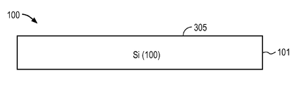
도 2는 일 실시예에 따라 미리 정해진 결정 방향을 따라 정렬되는 기판 상에 핀들이 형성된 후의 도 1과 유사한 뷰이다.
도 3은 일 실시예에 따라 절연층이 핀들 사이의 기판(101) 상에 피착되고, 또한 하드 마스크가 제거된 후의 도 2와 유사한 뷰이다.
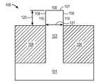
도 4는 일 실시예에 따라 도 3에 도시된 전자 디바이스 구조의 일부의 단면도이다.
도 5는 일 실시예에 따라 제2 결정 방향에 대응하는 제2 결정면을 따라 정렬되는 면을 노출시키기 위해 기판 상의 절연층 위의 핀을 변경(modifying)하는 것을 도해하는 도 4와 유사한 뷰이다.
도 6은 일 실시예에 따라 핀이 변경된 후의 도 5와 유사한 뷰이다.
도 7은 또 다른 실시예에 따라 절연층이 핀들 사이의 기판 상에 피착되고, 또한 하드 마스크가 제거된 후의 도 2에 도시된 전자 디바이스 구조의 일부의 단면도이다.
도 8은 또 다른 실시예에 따라 핀이 이방성으로 에칭된 후의 도 7과 유사한 뷰이다.
도 9는 일 실시예에 따라 절연층이 리세스된 후의 도 8과 유사한 뷰이다.
도 10은 일 실시예에 따라 도 6에 묘사된 대로의 핀을 갖는 전자 디바이스 구조의 사시도이다.
도 11은 일 실시예에 따라 도 9에 묘사된 대로의 핀을 갖는 전자 디바이스 구조의 사시도이다.
도 12는 일 실시예에 따라 도 8에 묘사된 대로의 핀을 갖는 전자 디바이스 구조의 사시도이다.
도 13은 일 실시예에 따라, 선택 사항인 핵형성/시드 층이 제2 결정 방향을 따라 정렬되는 핀의 면 상에 피착되고, 디바이스 층이 핵형성/시드 층 상에 피착되고, 및 분극 유도 층(polarization inducing layer)이 디바이스 층 상에 피착된 후의 도 6과 유사한 단면도이다.
도 14는 일 실시예에 따라, 선택 사항인 핵형성/시드 층이 제2 결정 방향을 따라 정렬되는 핀의 면 상에 피착되고, 디바이스 층이 핵형성/시드 층 상에 피착되고, 및 분극 유도 층이 디바이스 층 상에 피착된 후의 도 9와 유사한 단면도이다.
도 15는 도 16에 묘사된 대로의 전자 디바이스 구조의 사시도이다.
도 16은 또 다른 실시예에 따라, 디바이스 층이 제2 결정 방향을 따라 정렬되는 핀의 면 상에 피착되고, 및 분극 유도 층이 디바이스 층 상에 피착된 후의 도 6과 유사한 단면도이다.
도 17은 또 다른 실시예에 따라, 선택 사항인 핵형성/시드 층이 제2 결정 방향을 따라 정렬되는 핀의 면 상에 피착되고, 디바이스 층이 핵형성/시드 층 상에 피착되고, 및 분극 유도 층이 디바이스 층 상에 피착된 후의 도 6과 유사한 단면도이다.
도 18aa, 18ab 및 18ac는 본 명세서에서 기술되는 바와 같은 구조들의 실시예들의 "XSEM"(cross sectional scanning electron microscope) 사진들을 보여준다.
도 18ba, 18bb, 및 18bc는 핀들이 일 실시예에 따라 동일 시간 동안 TMAH 용액에서 에칭된 후에, 상이한 치수들을 갖는 핀들을 묘사하는 사진들을 보여준다.
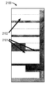
도 19는 일 실시예에 따라 고온 어닐링에 의한 핀들의 새 형상을 보여주는 사진(1901)의 뷰(1900)이다.
도 20a, 20b, 21a, 및 21b는 실시예에 따라 Si (111)과 유사한 평면들 상에서의 III-N 재료 층들의 성장을 도해한다.
도 22는 일 실시예에 따른 컴퓨팅 디바이스를 도해한다.
Claims (20)
- 전자 디바이스를 제조하기 위한 방법으로서:
제2 결정 방향을 따라 정렬되는 면을 형성하기 위해 제1 결정 방향을 따라 정렬되는 기판 상의 절연층 위의 핀을 변경(modifying)하는 단계; 및
상기 제2 결정 방향을 따라 정렬되는 상기 핀의 면 위에 디바이스 층을 피착하는 단계
를 포함하는 전자 디바이스 제조 방법. - 제1항에 있어서,
상기 핀과 상기 디바이스 층 사이에 핵형성 층을 피착하는 단계
를 더 포함하는 전자 디바이스 제조 방법. - 제1항에 있어서, 상기 핀을 변경하는 단계는 상기 제2 결정 방향을 따라 정렬되는 면을 노출시키기 위해 상기 핀을 에칭하는 단계를 포함하는
전자 디바이스 제조 방법. - 제1항에 있어서, 상기 핀을 변경하는 단계는 상기 제2 결정 방향을 따라 정렬되는 면을 형성하기 위해 상기 핀을 어닐링하는 단계를 포함하는
전자 디바이스 제조 방법. - 제1항에 있어서, 상기 기판은 실리콘을 포함하고, 상기 디바이스 층은 III-V족 재료를 포함하는 전자 디바이스 제조 방법.
- 제1항에 있어서,
2차원 전자 가스를 제공하도록 상기 디바이스 층 상에 분극 유도 층(polarization inducing layer)을 피착하는 단계
를 더 포함하는 전자 디바이스 제조 방법. - 제1항에 있어서,
상기 핀을 형성하기 위해 마스크를 통하여 상기 기판을 에칭하는 단계; 및
상기 기판 상에 상기 절연층을 피착하는 단계
를 더 포함하는 전자 디바이스 제조 방법. - 제1항에 있어서, 상기 제1 결정 방향은 <100> 결정 방향이고, 상기 제2 결정 방향은 <111> 결정 방향인 전자 디바이스 제조 방법.
- 제1항에 있어서, 상기 디바이스 층의 두께는 1 나노미터 내지 40 나노미터인 전자 디바이스 제조 방법.
- 제1항에 있어서, 상기 제1 핀의 폭은 상기 제1 핀의 높이보다 작은 전자 디바이스 제조 방법.
- 전자 디바이스로서:
제1 결정 방향을 따라 정렬되는 기판 상의 절연층 위의 핀 - 상기 핀은 제2 결정 방향을 따라 정렬되는 제1 면을 가짐-; 및
상기 제2 결정 방향을 따라 정렬되는 상기 핀의 제1 면 위에 피착되는 디바이스 층
을 포함하는 전자 디바이스. - 제11항에 있어서,
상기 핀과 상기 디바이스 층 사이의 핵형성 층
을 더 포함하는 전자 디바이스. - 제11항에 있어서,
2차원 전자 가스를 제공하기 위해 상기 디바이스 층 상에 분극 유도 층
을 더 포함하는 전자 디바이스. - 제11항에 있어서, 상기 핀은 상기 제1 면에 인접하여 상기 제2 결정 방향을 따라 정렬되는 제2 면을 갖는 전자 디바이스.
- 제11항에 있어서, 상기 핀은 삼각형 형상을 갖는 전자 디바이스.
- 제11항에 있어서, 상기 핀은 V 형상을 갖는 전자 디바이스.
- 제11항에 있어서, 상기 핀은 M 형상을 갖는 전자 디바이스.
- 제11항에 있어서, 상기 기판은 실리콘을 포함하고, 상기 디바이스 층은 III-V족 재료를 포함하는 전자 디바이스.
- 제11항에 있어서, 상기 제1 결정 방향은 <100> 결정 방향이고, 상기 제2 결정 방향은 <111> 결정 방향인 전자 디바이스.
- 제11항에 있어서, 상기 디바이스 층의 두께는 1 나노미터 내지 40 나노미터인 전자 디바이스.
Applications Claiming Priority (1)
| Application Number | Priority Date | Filing Date | Title |
|---|---|---|---|
| PCT/US2013/048757 WO2014209393A1 (en) | 2013-06-28 | 2013-06-28 | NANOSTRUCTURES AND NANOFEATURES WITH Si (111) PLANES ON Si (100) WAFERS FOR III-N EPITAXY |
Publications (1)
| Publication Number | Publication Date |
|---|---|
| KR20160029005A true KR20160029005A (ko) | 2016-03-14 |
Family
ID=52142514
Family Applications (1)
| Application Number | Title | Priority Date | Filing Date |
|---|---|---|---|
| KR1020157032507A Ceased KR20160029005A (ko) | 2013-06-28 | 2013-06-28 | III-N 에피택시를 위한 Si (100) 웨이퍼들 상의 Si (111) 평면들을 가진 나노구조들 및 나노피처들 |
Country Status (7)
| Country | Link |
|---|---|
| US (2) | US20160056244A1 (ko) |
| KR (1) | KR20160029005A (ko) |
| CN (1) | CN105531797A (ko) |
| DE (1) | DE112013007072T5 (ko) |
| GB (1) | GB2529953B (ko) |
| TW (2) | TWI582831B (ko) |
| WO (1) | WO2014209393A1 (ko) |
Families Citing this family (15)
| Publication number | Priority date | Publication date | Assignee | Title |
|---|---|---|---|---|
| DE102013103602A1 (de) * | 2013-04-10 | 2014-10-16 | Osram Opto Semiconductors Gmbh | Optoelektronischer Halbleiterchip und Verfahren zu seiner Herstellung |
| US9634185B2 (en) * | 2015-03-26 | 2017-04-25 | Imec Vzw | Optical semiconductor device and method for making the device |
| US9355914B1 (en) | 2015-06-22 | 2016-05-31 | International Business Machines Corporation | Integrated circuit having dual material CMOS integration and method to fabricate same |
| US9558943B1 (en) * | 2015-07-13 | 2017-01-31 | Globalfoundries Inc. | Stress relaxed buffer layer on textured silicon surface |
| US10658502B2 (en) * | 2015-12-24 | 2020-05-19 | Intel Corporation | Vertical III-N transistors with lateral overgrowth over a protruding III-N semiconductor structure |
| US10181526B2 (en) | 2016-06-02 | 2019-01-15 | Samsung Electronics Co., Ltd. | Field effect transistor including multiple aspect ratio trapping structures |
| US20180083000A1 (en) * | 2016-09-20 | 2018-03-22 | Qualcomm Incorporated | Fin epitaxy with lattice strain relaxation |
| US10263151B2 (en) * | 2017-08-18 | 2019-04-16 | Globalfoundries Inc. | Light emitting diodes |
| WO2019066789A1 (en) * | 2017-09-27 | 2019-04-04 | Intel Corporation | NANORUBAN III-N EPITAXIAL STRUCTURES FOR MANUFACTURING DEVICES |
| US10504747B2 (en) | 2017-09-29 | 2019-12-10 | Taiwan Semiconductor Manufacturing Company, Ltd. | Method of gap filling using conformal deposition-annealing-etching cycle for reducing seam void and bending |
| CN108231881A (zh) * | 2017-12-25 | 2018-06-29 | 中国电子科技集团公司第五十五研究所 | 图形化的Si(100)衬底GaN-HEMT外延片及其制备方法 |
| WO2019196021A1 (zh) * | 2018-04-10 | 2019-10-17 | 深圳大学 | 光电记忆器件、光电记忆读出器件及相机模组 |
| TWI683362B (zh) * | 2018-12-17 | 2020-01-21 | 許富翔 | 矽鰭片結構的修整方法 |
| US11145507B2 (en) * | 2019-12-16 | 2021-10-12 | Wafer Works Corporation | Method of forming gallium nitride film over SOI substrate |
| US11652105B2 (en) * | 2020-07-22 | 2023-05-16 | Taiwan Semiconductor Manufacturing Co., Ltd. | Epitaxy regions with large landing areas for contact plugs |
Family Cites Families (112)
| Publication number | Priority date | Publication date | Assignee | Title |
|---|---|---|---|---|
| JPS5244173A (en) * | 1975-10-06 | 1977-04-06 | Hitachi Ltd | Method of flat etching of silicon substrate |
| US4762382A (en) * | 1987-06-29 | 1988-08-09 | Honeywell Inc. | Optical interconnect circuit for GaAs optoelectronics and Si VLSI/VHSIC |
| US5040032A (en) * | 1988-02-09 | 1991-08-13 | Bell Communications Research, Inc. | Semiconductor superlattice heterostructures on non-planar substrates |
| US5114877A (en) * | 1991-01-08 | 1992-05-19 | Xerox Corporation | Method of fabricating quantum wire semiconductor laser via photo induced evaporation enhancement during in situ epitaxial growth |
| JPH06232099A (ja) * | 1992-09-10 | 1994-08-19 | Mitsubishi Electric Corp | 半導体装置の製造方法,半導体装置の製造装置,半導体レーザの製造方法,量子細線構造の製造方法,及び結晶成長方法 |
| JP3761918B2 (ja) * | 1994-09-13 | 2006-03-29 | 株式会社東芝 | 半導体装置の製造方法 |
| US5780343A (en) * | 1995-12-20 | 1998-07-14 | National Semiconductor Corporation | Method of producing high quality silicon surface for selective epitaxial growth of silicon |
| US5770475A (en) * | 1996-09-23 | 1998-06-23 | Electronics And Telecommunications Research Institute | Crystal growth method for compound semiconductor |
| WO2001043174A2 (en) * | 1999-12-13 | 2001-06-14 | North Carolina State University | Fabrication of gallium nitride layers on textured silicon substrates |
| US20020011612A1 (en) * | 2000-07-31 | 2002-01-31 | Kabushiki Kaisha Toshiba | Semiconductor device and method for manufacturing the same |
| KR100476940B1 (ko) * | 2003-06-20 | 2005-03-16 | 삼성전자주식회사 | 기판으로부터 수직으로 연장된 게이트 채널을 갖는디램기억 셀 및 그 제조방법 |
| KR100496891B1 (ko) * | 2003-08-14 | 2005-06-23 | 삼성전자주식회사 | 핀 전계효과 트랜지스터를 위한 실리콘 핀 및 그 제조 방법 |
| WO2005038931A1 (ja) * | 2003-10-20 | 2005-04-28 | Nec Corporation | 半導体装置及び半導体装置の製造方法 |
| US7385247B2 (en) * | 2004-01-17 | 2008-06-10 | Samsung Electronics Co., Ltd. | At least penta-sided-channel type of FinFET transistor |
| US7300837B2 (en) * | 2004-04-30 | 2007-11-27 | Taiwan Semiconductor Manufacturing Co., Ltd | FinFET transistor device on SOI and method of fabrication |
| JP4675585B2 (ja) * | 2004-06-22 | 2011-04-27 | シャープ株式会社 | 電界効果トランジスタ |
| US7262099B2 (en) * | 2004-08-23 | 2007-08-28 | Micron Technology, Inc. | Methods of forming field effect transistors |
| US6969644B1 (en) * | 2004-08-31 | 2005-11-29 | Texas Instruments Incorporated | Versatile system for triple-gated transistors with engineered corners |
| KR100601138B1 (ko) * | 2004-10-06 | 2006-07-19 | 에피밸리 주식회사 | Ⅲ-질화물 반도체 발광소자 및 그 제조 방법 |
| KR100849177B1 (ko) * | 2005-01-04 | 2008-07-30 | 삼성전자주식회사 | 패싯 채널들을 갖는 모스 트랜지스터를 채택하는 반도체집적회로 소자들 및 그 제조방법들 |
| JP2006196631A (ja) * | 2005-01-13 | 2006-07-27 | Hitachi Ltd | 半導体装置及びその製造方法 |
| US8324660B2 (en) * | 2005-05-17 | 2012-12-04 | Taiwan Semiconductor Manufacturing Company, Ltd. | Lattice-mismatched semiconductor structures with reduced dislocation defect densities and related methods for device fabrication |
| US7494858B2 (en) * | 2005-06-30 | 2009-02-24 | Intel Corporation | Transistor with improved tip profile and method of manufacture thereof |
| US8466490B2 (en) * | 2005-07-01 | 2013-06-18 | Synopsys, Inc. | Enhanced segmented channel MOS transistor with multi layer regions |
| US7586158B2 (en) * | 2005-07-07 | 2009-09-08 | Infineon Technologies Ag | Piezoelectric stress liner for bulk and SOI |
| US7666741B2 (en) * | 2006-01-17 | 2010-02-23 | International Business Machines Corporation | Corner clipping for field effect devices |
| JP4635897B2 (ja) * | 2006-02-15 | 2011-02-23 | 株式会社東芝 | 半導体装置及びその製造方法 |
| US7777250B2 (en) * | 2006-03-24 | 2010-08-17 | Taiwan Semiconductor Manufacturing Company, Ltd. | Lattice-mismatched semiconductor structures and related methods for device fabrication |
| US7566949B2 (en) * | 2006-04-28 | 2009-07-28 | International Business Machines Corporation | High performance 3D FET structures, and methods for forming the same using preferential crystallographic etching |
| US7582516B2 (en) * | 2006-06-06 | 2009-09-01 | International Business Machines Corporation | CMOS devices with hybrid channel orientations, and methods for fabricating the same using faceted epitaxy |
| JP2008141187A (ja) * | 2006-11-09 | 2008-06-19 | Matsushita Electric Ind Co Ltd | 窒化物半導体レーザ装置 |
| US20080237634A1 (en) * | 2007-03-30 | 2008-10-02 | International Business Machines Corporation | Crystallographic recess etch for embedded semiconductor region |
| FR2914783A1 (fr) * | 2007-04-03 | 2008-10-10 | St Microelectronics Sa | Procede de fabrication d'un dispositif a gradient de concentration et dispositif correspondant. |
| US8237151B2 (en) * | 2009-01-09 | 2012-08-07 | Taiwan Semiconductor Manufacturing Company, Ltd. | Diode-based devices and methods for making the same |
| US8927353B2 (en) * | 2007-05-07 | 2015-01-06 | Taiwan Semiconductor Manufacturing Co., Ltd. | Fin field effect transistor and method of forming the same |
| US8174073B2 (en) * | 2007-05-30 | 2012-05-08 | Taiwan Semiconductor Manufacturing Co., Ltd. | Integrated circuit structures with multiple FinFETs |
| US7956370B2 (en) * | 2007-06-12 | 2011-06-07 | Siphoton, Inc. | Silicon based solid state lighting |
| JP2009032955A (ja) * | 2007-07-27 | 2009-02-12 | Toshiba Corp | 半導体装置、およびその製造方法 |
| DE112008002387B4 (de) * | 2007-09-07 | 2022-04-07 | Taiwan Semiconductor Manufacturing Co., Ltd. | Struktur einer Mehrfachübergangs-Solarzelle, Verfahren zur Bildung einer photonischenVorrichtung, Photovoltaische Mehrfachübergangs-Zelle und Photovoltaische Mehrfachübergangs-Zellenvorrichtung, |
| US8188513B2 (en) * | 2007-10-04 | 2012-05-29 | Stc.Unm | Nanowire and larger GaN based HEMTS |
| US7727830B2 (en) * | 2007-12-31 | 2010-06-01 | Intel Corporation | Fabrication of germanium nanowire transistors |
| US8030666B2 (en) * | 2008-04-16 | 2011-10-04 | Taiwan Semiconductor Manufacturing Company, Ltd. | Group-III nitride epitaxial layer on silicon substrate |
| US8987092B2 (en) * | 2008-04-28 | 2015-03-24 | Spansion Llc | Methods for fabricating memory cells having fin structures with semicircular top surfaces and rounded top corners and edges |
| US20090283829A1 (en) * | 2008-05-13 | 2009-11-19 | International Business Machines Corporation | Finfet with a v-shaped channel |
| US8134169B2 (en) * | 2008-07-01 | 2012-03-13 | Taiwan Semiconductor Manufacturing Co., Ltd. | Patterned substrate for hetero-epitaxial growth of group-III nitride film |
| US20110114917A1 (en) * | 2008-07-21 | 2011-05-19 | Pan Shaoher X | Light emitting device |
| JP2010040973A (ja) * | 2008-08-08 | 2010-02-18 | Sony Corp | 半導体装置およびその製造方法 |
| TWI425558B (zh) * | 2008-08-11 | 2014-02-01 | 台灣積體電路製造股份有限公司 | 形成電路結構的方法 |
| US8268729B2 (en) * | 2008-08-21 | 2012-09-18 | International Business Machines Corporation | Smooth and vertical semiconductor fin structure |
| US8313967B1 (en) * | 2009-01-21 | 2012-11-20 | Stc.Unm | Cubic phase, nitrogen-based compound semiconductor films epitaxially grown on a grooved Si <001> substrate |
| US7906802B2 (en) * | 2009-01-28 | 2011-03-15 | Infineon Technologies Ag | Semiconductor element and a method for producing the same |
| JP4875115B2 (ja) * | 2009-03-05 | 2012-02-15 | 株式会社東芝 | 半導体素子及び半導体装置 |
| US8816391B2 (en) * | 2009-04-01 | 2014-08-26 | Taiwan Semiconductor Manufacturing Company, Ltd. | Source/drain engineering of devices with high-mobility channels |
| CN101853882B (zh) * | 2009-04-01 | 2016-03-23 | 台湾积体电路制造股份有限公司 | 具有改进的开关电流比的高迁移率多面栅晶体管 |
| WO2011004474A1 (ja) * | 2009-07-08 | 2011-01-13 | 株式会社 東芝 | 半導体装置及びその製造方法 |
| US8629478B2 (en) * | 2009-07-31 | 2014-01-14 | Taiwan Semiconductor Manufacturing Company, Ltd. | Fin structure for high mobility multiple-gate transistor |
| US8264021B2 (en) * | 2009-10-01 | 2012-09-11 | Taiwan Semiconductor Manufacturing Company, Ltd. | Finfets and methods for forming the same |
| US8350273B2 (en) * | 2009-08-31 | 2013-01-08 | Infineon Technologies Ag | Semiconductor structure and a method of forming the same |
| US8362575B2 (en) * | 2009-09-29 | 2013-01-29 | Taiwan Semiconductor Manufacturing Company, Ltd. | Controlling the shape of source/drain regions in FinFETs |
| US8415718B2 (en) * | 2009-10-30 | 2013-04-09 | Taiwan Semiconductor Manufacturing Company, Ltd. | Method of forming epi film in substrate trench |
| US8759203B2 (en) * | 2009-11-17 | 2014-06-24 | Taiwan Semiconductor Manufacturing Company, Ltd. | Growing III-V compound semiconductors from trenches filled with intermediate layers |
| US9087725B2 (en) * | 2009-12-03 | 2015-07-21 | Taiwan Semiconductor Manufacturing Company, Ltd. | FinFETs with different fin height and EPI height setting |
| US8598003B2 (en) * | 2009-12-21 | 2013-12-03 | Intel Corporation | Semiconductor device having doped epitaxial region and its methods of fabrication |
| US8722441B2 (en) * | 2010-01-21 | 2014-05-13 | Siphoton Inc. | Manufacturing process for solid state lighting device on a conductive substrate |
| US8674383B2 (en) * | 2010-01-21 | 2014-03-18 | Siphoton Inc. | Solid state lighting device on a conductive substrate |
| US20110233521A1 (en) * | 2010-03-24 | 2011-09-29 | Cree, Inc. | Semiconductor with contoured structure |
| US8729627B2 (en) * | 2010-05-14 | 2014-05-20 | Taiwan Semiconductor Manufacturing Company, Ltd. | Strained channel integrated circuit devices |
| US8609517B2 (en) * | 2010-06-11 | 2013-12-17 | Taiwan Semiconductor Manufacturing Company, Ltd. | MOCVD for growing III-V compound semiconductors on silicon substrates |
| KR101217209B1 (ko) * | 2010-10-07 | 2012-12-31 | 서울대학교산학협력단 | 발광소자 및 그 제조방법 |
| US8183134B2 (en) * | 2010-10-19 | 2012-05-22 | Taiwan Semiconductor Manufacturing Company, Ltd. | Semiconductor device and manufacturing method with improved epitaxial quality of III-V compound on silicon surfaces |
| US8709921B2 (en) * | 2010-11-15 | 2014-04-29 | Applied Materials, Inc. | Method for forming a semiconductor device using selective epitaxy of group III-nitride |
| US20120199888A1 (en) * | 2011-02-09 | 2012-08-09 | United Microelectronics Corporation | Fin field-effect transistor structure |
| US8217418B1 (en) * | 2011-02-14 | 2012-07-10 | Siphoton Inc. | Semi-polar semiconductor light emission devices |
| US8624292B2 (en) * | 2011-02-14 | 2014-01-07 | Siphoton Inc. | Non-polar semiconductor light emission devices |
| KR20120122776A (ko) * | 2011-04-29 | 2012-11-07 | 에스케이하이닉스 주식회사 | 반도체 소자 및 그의 제조 방법 |
| US9214538B2 (en) * | 2011-05-16 | 2015-12-15 | Eta Semiconductor Inc. | High performance multigate transistor |
| US8841701B2 (en) * | 2011-08-30 | 2014-09-23 | Taiwan Semiconductor Manufacturing Company, Ltd. | FinFET device having a channel defined in a diamond-like shape semiconductor structure |
| US8946829B2 (en) * | 2011-10-14 | 2015-02-03 | Taiwan Semiconductor Manufacturing Company, Ltd. | Selective fin-shaping process using plasma doping and etching for 3-dimensional transistor applications |
| US20130093062A1 (en) * | 2011-10-18 | 2013-04-18 | Ying-Chih Lin | Semiconductor structure and process thereof |
| DE112011105751B4 (de) * | 2011-10-18 | 2024-05-08 | Intel Corporation | Antifuse-Element unter Verwendung von nicht-planarer Topologie |
| KR20130047813A (ko) * | 2011-10-31 | 2013-05-09 | 삼성전자주식회사 | Iii-v족 화합물 반도체층을 포함하는 반도체 소자 및 그 제조방법 |
| KR101867999B1 (ko) * | 2011-10-31 | 2018-06-18 | 삼성전자주식회사 | Iii-v족 물질층을 형성하는 방법, iii-v족 물질층을 포함하는 반도체 소자 및 그 제조방법 |
| KR101805634B1 (ko) * | 2011-11-15 | 2017-12-08 | 삼성전자 주식회사 | Ⅲ-ⅴ족 배리어를 포함하는 반도체 소자 및 그 제조방법 |
| US9006069B2 (en) * | 2011-12-19 | 2015-04-14 | Intel Corporation | Pulsed laser anneal process for transistors with partial melt of a raised source-drain |
| KR20160134872A (ko) * | 2011-12-19 | 2016-11-23 | 인텔 코포레이션 | 비평면 iii-n 트랜지스터 |
| US8629038B2 (en) * | 2012-01-05 | 2014-01-14 | Taiwan Semiconductor Manufacturing Company, Ltd. | FinFETs with vertical fins and methods for forming the same |
| US8546891B2 (en) * | 2012-02-29 | 2013-10-01 | Taiwan Semiconductor Manufacturing Company, Ltd. | Fin profile structure and method of making same |
| US8629512B2 (en) * | 2012-03-28 | 2014-01-14 | Taiwan Semiconductor Manufacturing Company, Ltd. | Gate stack of fin field effect transistor with slanted sidewalls |
| US9012286B2 (en) * | 2012-04-12 | 2015-04-21 | Globalfoundries Inc. | Methods of forming FinFET semiconductor devices so as to tune the threshold voltage of such devices |
| US9368388B2 (en) * | 2012-04-13 | 2016-06-14 | Taiwan Semiconductor Manufacturing Company, Ltd. | Apparatus for FinFETs |
| US9559189B2 (en) * | 2012-04-16 | 2017-01-31 | United Microelectronics Corp. | Non-planar FET |
| WO2013165620A1 (en) * | 2012-05-04 | 2013-11-07 | Stc.Unm | Growth of cubic crystalline phase structure on silicon substrates and devices comprising the cubic crystalline phase structure |
| US8669147B2 (en) * | 2012-06-11 | 2014-03-11 | Globalfoundries Inc. | Methods of forming high mobility fin channels on three dimensional semiconductor devices |
| US8729634B2 (en) * | 2012-06-15 | 2014-05-20 | Taiwan Semiconductor Manufacturing Company, Ltd. | FinFET with high mobility and strain channel |
| KR101909204B1 (ko) * | 2012-06-25 | 2018-10-17 | 삼성전자 주식회사 | 내장된 스트레인-유도 패턴을 갖는 반도체 소자 및 그 형성 방법 |
| US8883570B2 (en) * | 2012-07-03 | 2014-11-11 | Taiwan Semiconductor Manufacturing Company, Ltd. | Multi-gate FETs and methods for forming the same |
| US9142400B1 (en) * | 2012-07-17 | 2015-09-22 | Stc.Unm | Method of making a heteroepitaxial layer on a seed area |
| US8729607B2 (en) * | 2012-08-27 | 2014-05-20 | Kabushiki Kaisha Toshiba | Needle-shaped profile finFET device |
| US9064709B2 (en) * | 2012-09-28 | 2015-06-23 | Intel Corporation | High breakdown voltage III-N depletion mode MOS capacitors |
| KR20140052734A (ko) * | 2012-10-25 | 2014-05-07 | 삼성전자주식회사 | 반도체 소자 및 이의 제조 방법 |
| US8768271B1 (en) * | 2012-12-19 | 2014-07-01 | Intel Corporation | Group III-N transistors on nanoscale template structures |
| US8785907B2 (en) * | 2012-12-20 | 2014-07-22 | Intel Corporation | Epitaxial film growth on patterned substrate |
| CN103943498B (zh) * | 2013-01-22 | 2016-08-10 | 中芯国际集成电路制造(上海)有限公司 | 三维量子阱晶体管及其形成方法 |
| US9196709B2 (en) * | 2013-02-01 | 2015-11-24 | Taiwan Semiconductor Manufacturing Company, Ltd. | Methods for forming semiconductor regions in trenches |
| US9123633B2 (en) * | 2013-02-01 | 2015-09-01 | Taiwan Semiconductor Manufacturing Company, Ltd. | Methods for forming semiconductor regions in trenches |
| US9054044B2 (en) * | 2013-03-07 | 2015-06-09 | Globalfoundries Inc. | Method for forming a semiconductor device and semiconductor device structures |
| US9159832B2 (en) * | 2013-03-08 | 2015-10-13 | Taiwan Semiconductor Manufacturing Company, Ltd. | Semiconductor fin structures and methods for forming the same |
| CN104218082B (zh) * | 2013-06-04 | 2017-08-25 | 中芯国际集成电路制造(上海)有限公司 | 高迁移率鳍型场效应晶体管及其制造方法 |
| US9275861B2 (en) * | 2013-06-26 | 2016-03-01 | Globalfoundries Inc. | Methods of forming group III-V semiconductor materials on group IV substrates and the resulting substrate structures |
| US20150014808A1 (en) * | 2013-07-11 | 2015-01-15 | United Microelectronics Corp. | Semiconductor structure and fabrication method thereof |
| US9240342B2 (en) * | 2013-07-17 | 2016-01-19 | Globalfoundries Inc. | Methods of forming replacement fins for a FinFET semiconductor device by performing a replacement growth process |
| EP3050110A4 (en) * | 2013-09-25 | 2017-05-17 | Intel Corporation | Forming iii-v device structures on (111) planes of silicon fins |
-
2013
- 2013-06-28 WO PCT/US2013/048757 patent/WO2014209393A1/en not_active Ceased
- 2013-06-28 CN CN201380077010.9A patent/CN105531797A/zh active Pending
- 2013-06-28 US US14/779,257 patent/US20160056244A1/en not_active Abandoned
- 2013-06-28 KR KR1020157032507A patent/KR20160029005A/ko not_active Ceased
- 2013-06-28 GB GB1520313.6A patent/GB2529953B/en active Active
- 2013-06-28 DE DE112013007072.3T patent/DE112013007072T5/de not_active Withdrawn
-
2014
- 2014-06-23 TW TW104139661A patent/TWI582831B/zh not_active IP Right Cessation
- 2014-06-23 TW TW103121562A patent/TWI517217B/zh not_active IP Right Cessation
-
2017
- 2017-04-06 US US15/481,200 patent/US20170213892A1/en not_active Abandoned
Also Published As
| Publication number | Publication date |
|---|---|
| TW201517128A (zh) | 2015-05-01 |
| TW201626440A (zh) | 2016-07-16 |
| CN105531797A (zh) | 2016-04-27 |
| DE112013007072T5 (de) | 2016-01-28 |
| GB2529953B (en) | 2020-04-01 |
| US20160056244A1 (en) | 2016-02-25 |
| WO2014209393A1 (en) | 2014-12-31 |
| TWI582831B (zh) | 2017-05-11 |
| US20170213892A1 (en) | 2017-07-27 |
| GB2529953A (en) | 2016-03-09 |
| GB201520313D0 (en) | 2015-12-30 |
| TWI517217B (zh) | 2016-01-11 |
Similar Documents
| Publication | Publication Date | Title |
|---|---|---|
| KR20160029005A (ko) | III-N 에피택시를 위한 Si (100) 웨이퍼들 상의 Si (111) 평면들을 가진 나노구조들 및 나노피처들 | |
| US10475888B2 (en) | Integration of III-V devices on Si wafers | |
| CN105874587B (zh) | Si沟槽中的ⅲ-n器件 | |
| US10269971B2 (en) | Semiconductor devices and FinFETs | |
| KR102106348B1 (ko) | 선택적 에피텍시 및 컨포멀 에피텍시의 조합에 의한 cmos용의 패터닝된 실리콘 기판 상의 비실리콘 디바이스 이종층들 | |
| TWI544636B (zh) | 使用選擇式磊晶成長整合vlsi相容性鰭狀結構與在其上製作裝置 | |
| KR102245485B1 (ko) | 선택적 에피택시 동안 측벽 결함을 방지하는 방법 및 구조 | |
| US10475706B2 (en) | Making a defect free fin based device in lateral epitaxy overgrowth region | |
| CN107660310B (zh) | 异质外延n型晶体管与p型晶体管的基于阱的集成 |
Legal Events
| Date | Code | Title | Description |
|---|---|---|---|
| PA0105 | International application |
St.27 status event code: A-0-1-A10-A15-nap-PA0105 |
|
| P11-X000 | Amendment of application requested |
St.27 status event code: A-2-2-P10-P11-nap-X000 |
|
| P13-X000 | Application amended |
St.27 status event code: A-2-2-P10-P13-nap-X000 |
|
| PG1501 | Laying open of application |
St.27 status event code: A-1-1-Q10-Q12-nap-PG1501 |
|
| A201 | Request for examination | ||
| PA0201 | Request for examination |
St.27 status event code: A-1-2-D10-D11-exm-PA0201 |
|
| P22-X000 | Classification modified |
St.27 status event code: A-2-2-P10-P22-nap-X000 |
|
| E902 | Notification of reason for refusal | ||
| PE0902 | Notice of grounds for rejection |
St.27 status event code: A-1-2-D10-D21-exm-PE0902 |
|
| E13-X000 | Pre-grant limitation requested |
St.27 status event code: A-2-3-E10-E13-lim-X000 |
|
| P11-X000 | Amendment of application requested |
St.27 status event code: A-2-2-P10-P11-nap-X000 |
|
| P13-X000 | Application amended |
St.27 status event code: A-2-2-P10-P13-nap-X000 |
|
| E601 | Decision to refuse application | ||
| PE0601 | Decision on rejection of patent |
St.27 status event code: N-2-6-B10-B15-exm-PE0601 |
|
| P22-X000 | Classification modified |
St.27 status event code: A-2-2-P10-P22-nap-X000 |
|
| P22-X000 | Classification modified |
St.27 status event code: A-2-2-P10-P22-nap-X000 |